ICGOO在线商城 > 光电元件 > LED - 电路板指示器,阵列,发光条,条形图 > HLMP-1719-A00A2
/HLMP-1719-A00A2.jpg)
 Datasheet下载
- 型号: HLMP-1719-A00A2
- 制造商: Avago Technologies
- 库位|库存: xxxx|xxxx
- 要求:
| 数量阶梯 | 香港交货 | 国内含税 |
| +xxxx | $xxxx | ¥xxxx |
查看当月历史价格
查看今年历史价格
HLMP-1719-A00A2产品简介:
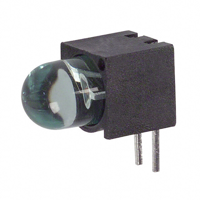
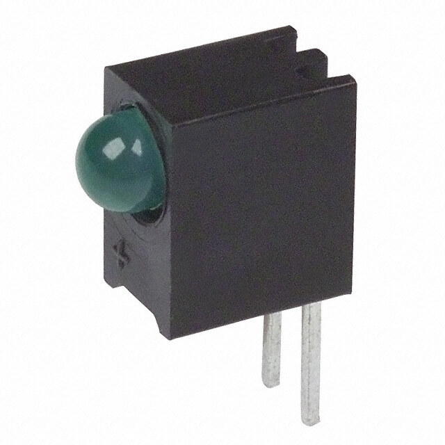
ICGOO电子元器件商城为您提供HLMP-1719-A00A2由Avago Technologies设计生产,在icgoo商城现货销售,并且可以通过原厂、代理商等渠道进行代购。 HLMP-1719-A00A2价格参考。Avago TechnologiesHLMP-1719-A00A2封装/规格:LED - 电路板指示器,阵列,发光条,条形图, LED Circuit Board Indicator Single Yellow Diffused, Tinted 1.8V 2mA Round with Domed Top, 3mm (T-1) Through Hole, Right Angle。您可以下载HLMP-1719-A00A2参考资料、Datasheet数据手册功能说明书,资料中有HLMP-1719-A00A2 详细功能的应用电路图电压和使用方法及教程。
| 参数 | 数值 |
| 产品目录 | |
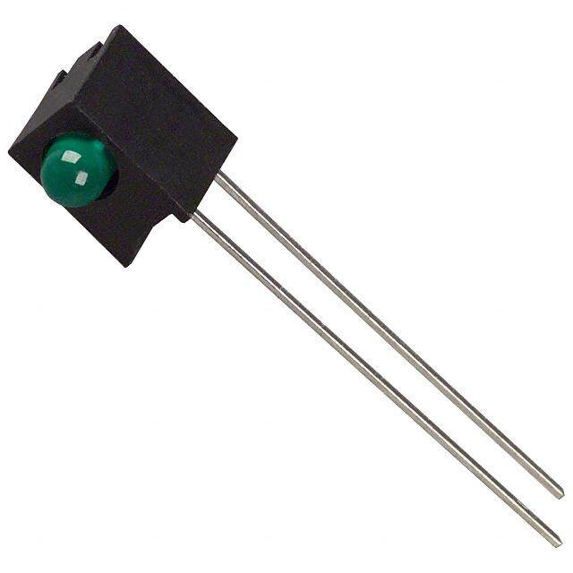
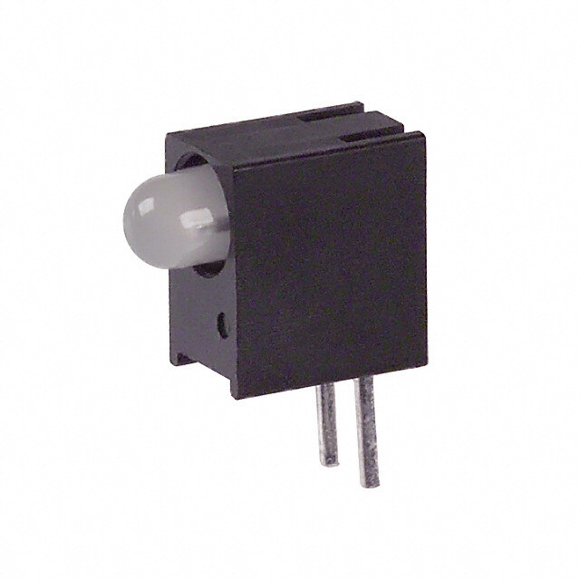
| 描述 | LED 3MM GAP DIFF YLW RA HOUSING标准LED-通孔 Yellow Diffused 585nm 2.1mcd |
| 产品分类 | |
| LED大小 | T-1 |
| 品牌 | Avago Technologies |
| 产品手册 | http://www.avagotech.com/docs/AV02-1557EN |
| 产品图片 |
|
| rohs | 符合RoHS无铅 / 符合限制有害物质指令(RoHS)规范要求 |
| 产品系列 | LED发射器,标准LED-通孔,Avago Technologies HLMP-1719-A00A2HLMP-1719 |
| 数据手册 | http://www.avagotech.com/docs/AV02-1557ENhttp://www.avagotech.com/docs/AV02-0780EN |
| 产品型号 | HLMP-1719-A00A2 |
| 产品目录绘图 |
|
| 产品种类 | 标准LED-通孔 |
| 光强度 | 2.1 mcd |
| 其它名称 | 516-1895 |
| 包装 | 散装 |
| 商标 | Avago Technologies |
| 安装类型 | 通孔,直角 |
| 安装风格 | Through Hole |
| 封装 | Bulk |
| 工厂包装数量 | 2000 |
| 显示角 | 50 deg |
| 最大工作温度 | + 100 C |
| 最小工作温度 | - 40 C |
| 标准包装 | 2,000 |
| 正向电压 | 1.8 V |
| 正向电流 | 2 mA |
| 毫烛光等级 | 2.1mcd |
| 波长-峰值 | 585nm |
| 波长/色温 | 585 nm |
| 照明颜色 | Yellow |
| 电流 | 2mA |
| 视角 | - |
| 透镜尺寸 | 3 mm |
| 透镜形状 | Dome |
| 透镜样式/尺寸 | 圆形,带圆顶,3mm |
| 透镜类型 | 散射,有色 |
| 透镜颜色/类型 | Tinted, Diffused |
| 配置 | 单一 |
| 颜色 | 黄 |
| 额定电压 | 1.8V |


- 商务部:美国ITC正式对集成电路等产品启动337调查
- 曝三星4nm工艺存在良率问题 高通将骁龙8 Gen1或转产台积电
- 太阳诱电将投资9.5亿元在常州建新厂生产MLCC 预计2023年完工
- 英特尔发布欧洲新工厂建设计划 深化IDM 2.0 战略
- 台积电先进制程称霸业界 有大客户加持明年业绩稳了
- 达到5530亿美元!SIA预计今年全球半导体销售额将创下新高
- 英特尔拟将自动驾驶子公司Mobileye上市 估值或超500亿美元
- 三星加码芯片和SET,合并消费电子和移动部门,撤换高东真等 CEO
- 三星电子宣布重大人事变动 还合并消费电子和移动部门
- 海关总署:前11个月进口集成电路产品价值2.52万亿元 增长14.8%

PDF Datasheet 数据手册内容提取
HLMP-4700, HLMP-4719, HLMP-4740 HLMP-1700, HLMP-1719, HLMP-1790 T-13/ (5 mm), T-1 (3 mm), Low Current LED Lamps 4 Data Sheet Description Features These tinted diffused LED lamps are designed and opti- • Low power mized specifically for low DC current operation. Luminous • High efficiency intensity and forward voltage are tested at 2 mA to assure • CMOS-MOS compatible consistent brightness at TTL output current levels. • TTL compatible Applications • Wide viewing angle • Low power DC circuits • Choice of package styles • Telecommunications indicators • Choice of colors • Portable equipment • Keyboard indicators Package Dimensions 6.10 (0.240) 0.89 (0.035) SQUARE TYP. 5.59 (0.220) 0.64 (0.025) 0.55 (0.022) 0.65 (0.026) MAX. 0.40 (0.016) 5.08 (0.200) 4.57 (0.180) CATHODE 9.19 (0.362) 1.27(0.050) 2.54 (0.100) NOM. 8.43 (0.332) 25.40 (1.00) NOM. MIN. A - HLMP-4700, -4719, -4740 1.14 (.045) 0.51 (.020) 2.79 (.110) 24.1 (.95) MIN. 2.29 (.090) 3.43 (.135) CATHODE 1.52 (.060) 2.92 (.115) 0.65 (0.026) MAX. 1.02 (.040) 3.17 (.125) ∅ 2.67 (.105) (0.022) 0.55 SQUARE TYP. 4.70 (.185) (0.016) 0.40 4.19 (.165) 6.35 (.250) 5.58 (.220) B - HLMP-1700, -1719, -1790 Notes: 1. All dimensions are in mm (inches). 2. An epoxy meniscus may extend about 1 mm (0.040") down the leads. 3. For PCB hole recommendations, see the Precautions section.
Selection Guide Luminous Intensity Iv (mcd) at 2 mA Device Package Package Description Color HLMP- Min. Typ. Max. 2q1/2 Outline T-1 3/4 Tinted Diffused Red 4700 1.5 2.3 – 50 A 4700-C00xx 1.5 2.3 – 4700-CD0FH 1.5 2.3 4.2 Yellow 4719 0.9 2.1 – 4719-A00xx 0.9 2.1 – Green 4740 1.0 2.3 – 4740-A00xx 1.0 2.3 – 4740-AB000 1.0 2.3 3.2 T-1 Tinted Diffused Red 1700 0.8 2.1 – 50 B 1700-B00xx 0.8 2.1 – Yellow 1719 0.9 2.1 – 1719-A00xx 0.9 2.1 – 1719-ABB00 0.9 2.1 2.8 Green 1790 1.0 2.3 – 1790-A00xx 1.0 2.3 – 1790-AB0FH 1.0 2.4 3.2 Note: 1. q1/2 is the typical off-axis angle at which the luminous intensity is half the axial luminous intensity. 2
Part Numbering System HLMP – X 7 XX - X X X XX Mechanical Option 00: Bulk 01: Tape & Reel, Crimped Leads 02, BH: Tape & Reel, Straight Leads A1, B1: Right Angle Housing, Uneven Leads A2, B2: Right Angle Housing, Even Leads FH: 2 Iv bins select with Inventory Control Color Bin Options 0: Full color bin distribution B: Color bins 2 & 3 only Maximum Iv Bin Options 0: Open (No. max. limit) Others: Please refer to the Iv bin Table Minimum Iv Bin Options Please refer to the Iv Bin Table Color Options 00: GaP HER 19: GaP Yellow 40: GaP Green 90: GaP Green Package Options 4: T-13/4 (5 mm) 1: T-1 (3 mm) 3
Electrical/Optical Characteristics at T = 25°C A Symbol Description T-13/4 T-1 Min. Typ. Max. Units Test Conditions VF Forward Voltage 4700 1700 1.7 2.0 V 2 mA 4719 1719 1.8 2.5 4740 1790 1.9 2.2 VR Reverse Breakdown 4700 1700 5.0 V IR = 50 μA Voltage 4719 1719 5.0 4740 1790 5.0 ld Dominant 4700 1700 626 nm Note 1 Wavelength 4719 1719 585 4740 1790 569 Dl1/2 Spectral Line 4700 1700 40 nm Halfwidth 4719 1719 36 4740 1790 28 tS Speed of Response 4700 1700 90 ns 4719 1719 90 4740 1790 500 C Capacitance 4700 1700 11 pF VF = 0, 4719 1719 15 f = 1 MHz 4740 1790 18 RqJ-PIN Thermal Resistance 4700 1700 260[3] °C/W Junction to Cathode Lead 4719 1719 290[4] 4740 1790 lPEAK Peak Wavelength 4700 1700 635 nm Measurement at Peak 4740 1790 565 hV Luminous Efficacy 4700 1700 145 lumens/watt Note 2 4719 1719 500 4740 1790 595 Notes: 1. The dominant wavelength, ld, is derived from the CIE chromaticity diagram and represents the single wavelength which defines the color of the device. 2. The radiant intensity, Ie, in watts per steradian, may be found from the equation Ie = IV/hV, where IV is the luminous intensity in candelas and hV is luminous efficacy in lumens/watt. 3. T-13/4. 4. T-1. 4
Absolute Maximum Ratings Parameter Maximum Rating Units Power Dissipation Red 14 mW (Derate linearly from 92°C at 1.0 mA/°C) Yellow 17.5 Green 15.4 DC and Peak Forward Current 7 mA Transient Forward Current (10 μs Pulse)[1] 500 mA Reverse Voltage (IR = 50 μA) 5.0 V Operating Temperature Range Red/Yellow -40 to 100 °C Green -20 to 100 °C Storage Temperature Range -40 to +100 °C Notes: 1. The transient peak current is the maximum non-recurring peak current the devices can withstand without damaging the LED die and wire bonds. It is not recommended that the device be operated at peak currents beyond the Absolute Maximum Peak Forward Current. 1.0 TA = 25° C GREEN YELLOW Y T NSI RED E T E IN 0.5 V TI A L E R 0 500 550 600 650 700 750 WAVELENGTH – nm Figure 1. Relative intensity vs. wavelength. 10 10.0 T - 25°C A Y 8 SIT 8.0 A TENmA) YELLOW m RED N2 DC CURRENT – 64 YEGLRLEOEWN VE LUMINOUS IORMALIZED AT 46..00 GREEN RED ATI(N 2 EL 2.0 R 0 0 0 0.5 1.0 1.5 2.0 2.5 0 2 4 6 8 10 VOLTAGE – V IDC -DC CURRENT PER LED - mA Figure 2. Forward current vs. forward voltage. Figure 3. Relative luminous intensity vs. forward current. 5
20° 10° 0° 1.0 20° 10° 0° 1.0 30° 30° 40° 0.8 40° 0.8 70°60° 50° 00..64 RELATIVE INTENSITY 70°60° 50° 00..64 RELATIVE INTENSITY 80° 0.2 80° 0.2 90° 10° 20° 30° 40° 50° 60° 70° 80° 90°1000°.0 90° 10° 20° 30° 40° 50° 60° 70° 80° 90°1000°.0 Figure 4. Relative luminous intensity vs. angular displacement for T-13/4 lamp. Figure 5. Relative llluminous intensity vs. angular displacement for T-1 lamp. Intensity Bin Limits Intensity Bin Limits Intensity Range (mcd) Intensity Range (mcd) Color Bin Min. Max. Color Bin Min. Max. Red B 0.9 1.5 Yellow A 1.0 1.6 C 1.5 2.4 B 1.6 2.5 D 2.4 3.8 C 2.5 4.0 E 3.8 6.1 D 4.0 6.5 F 6.1 9.7 E 6.5 10.3 G 9.7 15.5 F 10.3 16.6 H 15.5 24.8 G 16.6 26.5 I 24.8 39.6 H 26.5 42.3 J 39.6 63.4 I 42.3 67.7 K 63.4 101.5 J 67.7 108.2 L 101.5 162.4 K 108.2 173.2 M 162.4 234.6 L 173.2 250.0 N 234.6 340.0 M 250.0 360.0 O 340.0 540.0 N 360.0 510.0 P 540.0 850.0 O 510.0 800.0 Q 850.0 1200.0 P 800.0 1250.0 R 1200.0 1700.0 Q 1250.0 1800.0 S 1700.0 2400.0 R 1800.0 2900.0 T 2400.0 3400.0 S 2900.0 4700.0 U 3400.0 4900.0 T 4700.0 7200.0 V 4900.0 7100.0 U 7200.0 11700.0 W 7100.0 10200.0 V 11700.0 18000.0 X 10200.0 14800.0 W 18000.0 27000.0 Y 14800.0 21400.0 Maximum tolerance for each bin limit is ±18%. Z 21400.0 30900.0 Maximum tolerance for each bin limit is ±18%. 6
Intensity Bin Limits Color Categories Intensity Range (mcd) Lambda (nm) Color Bin Min. Max. Color Category # Min. Max. Green A 1.1 1.8 6 561.5 564.5 B 1.8 2.9 5 564.5 567.5 C 2.9 4.7 Green 4 567.5 570.5 D 4.7 7.6 3 570.5 573.5 E 7.6 12.0 2 573.5 576.5 F 12.0 19.1 1 582.0 584.5 G 19.1 30.7 3 584.5 587.0 H 30.7 49.1 Yellow 2 587.0 589.5 I 49.1 78.5 4 589.5 592.0 J 78.5 125.7 5 592.0 593.0 K 125.7 201.1 Tolerance for each bin limit is ±0.5 nm. L 201.1 289.0 M 289.0 417.0 N 417.0 680.0 O 680.0 1100.0 P 1100.0 1800.0 Q 1800.0 2700.0 R 2700.0 4300.0 S 4300.0 6800.0 T 6800.0 10800.0 U 10800.0 16000.0 V 16000.0 25000.0 W 25000.0 40000.0 Maximum tolerance for each bin limit is ±18%. Mechanical Option Matrix Mechanical Option Code Definition 00 Bulk Packaging, minimum increment 500 pc/bag 01 Tape & Reel, crimped leads, min. increment 1300 pcs/bag for T-1 3/4, 1800 pcs/bag for T-1 02 Tape & Reel, straight leads, min. increment 1300 pcs/bag for T-1 3/4, 1800 pcs/bag for T-1 A1 T-1, Right Angle Housing, uneven leads, minimum increment 500 pcs/bag A2 T-1, Right Angle Housing, even leads, minimum increment 500 pcs/bag B1 T-1 3/4, Right Angle Housing, uneven leads, minimum increment 500 pcs/bag B2 T-1 3/4, Right Angle Housing, even leads, minimum increment 500 pcs/bag BH T-1, Tape & Reel, straight leads, minimum increment 2000 pcs/bag FH Devices that require inventory control and 2 Iv bin select R1 Tape & Reel, crimped leads, reeled counter clockwise, cathode lead leaving the reel first Notes: All categories are established for classification of products. Products may not be available in all categories. Please contact your local Avago representative for further clarification/information. 7
Precautions: Lead Forming: • The leads of an LED lamp may be preformed or cut to • Wave soldering parameters must be set and maintained length prior to insertion and soldering on PC board. according to the recommended temperature and dwell time. Customer is advised to perform daily check on the • For better control, it is recommended to use proper soldering profile to ensure that it is always conforming tool to precisely form and cut the leads to applicable to recommended soldering conditions. length rather than doing it manually. Note: • If manual lead cutting is necessary, cut the leads after 1. PCB with different size and design (component density) will have the soldering process. The solder connection forms a different heat mass (heat capacity). This might cause a change in mechanical ground which prevents mechanical stress temperature experienced by the board if same wave soldering setting is used. So, it is recommended to re-calibrate the soldering due to lead cutting from traveling into LED package. profile again before loading a new type of PCB. This is highly recommended for hand solder operation, 2. Customer is advised to take extra precaution during wave soldering as the excess lead length also acts as small heat sink. to ensure that the maximum wave temperature does not exceed 250°C and the solder contact time does not exceeding 3sec. Over- Soldering and Handling: stressing the LED during soldering process might cause premature • Care must be taken during PCB assembly and soldering failure to the LED due to delamination. process to prevent damage to the LED component. • Any alignment fixture that is being applied during wave soldering should be loosely fitted and should • LED component may be effectively hand soldered not apply weight or force on LED. Non metal material to PCB. However, it is only recommended under is recommended as it will absorb less heat during wave unavoidable circumstances such as rework. The closest soldering process. manual soldering distance of the soldering heat source (soldering iron’s tip) to the body is 1.59mm. Soldering • At elevated temperature, LED is more susceptible to the LED using soldering iron tip closer than 1.59mm mechanical stress. Therefore, PCB must allowed to cool might damage the LED. down to room temperature prior to handling, which 1.59 mm includes removal of alignment fixture or pallet. • If PCB board contains both through hole (TH) LED and other surface mount components, it is recommended that surface mount components be soldered on the • ESD precaution must be properly applied on the top side of the PCB. If surface mount need to be on the soldering station and personnel to prevent ESD bottom side, these components should be soldered damage to the LED component that is ESD sensitive. using reflow soldering prior to insertion the TH LED. Do refer to Avago application note AN 1142 for details. • Recommended PC board plated through holes (PTH) The soldering iron used should have grounded tip to size for LED component leads. ensure electrostatic charge is properly grounded. LED Component Diagonal Plated Through- • Recommended soldering condition: Lead Size Hole Diameter Wave Manual Solder Lead size (typ.) 0.45 × 0.45 mm 0.636 mm 0.98 to 1.08 mm Soldering[1],[2] Dipping (0.018 × 0.018 in.) (0.025 in) (0.039 to 0.043 in) Pre-heat Temperature 105°C Max. – Dambar shear- 0.65 mm 0.919 mm Pre-heat Time 60 sec Max. – off area (max.) (0.026 in) (0.036 in) Peak Temperature 250°C Max. 260°C Max. Lead size (typ.) 0.50 × 0.50 mm 0.707 mm 1.05 to 1.15 mm Dwell Time 3 sec Max. 5 sec Max. (0.020 × 0.020 in.) (0.028 in) (0.041 to 0.045 in) Note: Dambar shear- 0.70 mm 0.99 mm 1) Above conditions refers to measurement with thermocouple off area (max.) (0.028 in) (0.039 in) mounted at the bottom of PCB. Note: Refer to application note AN1027 for more information on 2) It is recommended to use only bottom preheaters in order to soldering LED components. reduce thermal stress experienced by LED. • Over-sizing the PTH can lead to twisted LED after clinching. On the other hand under sizing the PTH can cause difficulty inserting the TH LED. Refer to application note AN5334 for more information about soldering and handling of TH LED lamps. 8
Example of Wave Soldering Temperature Profile for TH LED Recommended solder: LAMINAR TURBULENT WAVE Sn63 (Leaded solder alloy) 250 HOT AIR KNIFE SAC305 (Lead free solder alloy) Flux: Rosin flux Solder bath temperature: 200 245°C± 5°C (maximum peak temperature = 250°C) C) E (° Dwell time: 1.5 sec – 3.0 sec (maximum = 3sec) R TU 150 Note: Allow for board to be sufficiently cooled to A R room temperature before exerting mechanical force. E MP Recommended solder: TE Sn63 (Leaded solder alloy) 100 SAC305 (Lead free solder alloy) Flux: Rosin flux 50 Solder bath temperature: 245°C± 5°C (maximum peak temperature = 250°C) PREHEAT Dwell time: 1.5 sec – 3.0 sec (maximum = 3sec) 0 10 20 30 40 50 60 70 80 90 100 Note: Allow for board to be sufficiently cooled to room temperature before exerting mechanical force. TIME (SECONDS ) Packaging Label: (i) Avago Mother Label: (Available on packaging box of ammo pack and shipping box) (1P) Item: Part Number STANDARD LABEL LS0002 RoHS Compliant e3 max temp 250C (1T) Lot: Lot Number (Q) QTY: Quantity LPN: CAT: Intensity Bin (9D)MFG Date: Manufacturing Date BIN: Color Bin (P) Customer Item: (V) Vendor ID: (9D) Date Code: Date Code DeptID: Made In: Country of Origin RoHS Compliant Lamps Baby Label e3 max temp 250C (1P) PART #: Part Number (1T) LOT #: Lot Number 9 (9D)MFG DATE: Manufacturing Date QUANTITY: Packing Quantity C/O: Country of Origin Customer P/N: CAT: Intensity Bin Supplier Code: BIN: Color Bin DATECODE: Date Code
(1P) Item: Part Number STANDARD LABEL LS0002 RoHS Compliant e3 max temp 250C (1T) Lot: Lot Number (Q) QTY: Quantity LPN: CAT: Intensity Bin (9D)MFG Date: Manufacturing Date BIN: Color Bin (P) Customer Item: (V) Vendor ID: (9D) Date Code: Date Code DeptID: Made In: Country of Origin (ii) Avago Baby Label (Only available on bulk packaging) RoHS Compliant Lamps Baby Label e3 max temp 250C (1P) PART #: Part Number (1T) LOT #: Lot Number (9D)MFG DATE: Manufacturing Date QUANTITY: Packing Quantity C/O: Country of Origin Customer P/N: CAT: Intensity Bin Supplier Code: BIN: Color Bin DATECODE: Date Code For product information and a complete list of distributors, please go to our web site: www.avagotech.com Avago, Avago Technologies, and the A logo are trademarks of Avago Technologies in the United States and other countries. Data subject to change. Copyright © 2005-2014 Avago Technologies. All rights reserved. Obsoletes 5989-4256EN AV02-1557EN - July 24, 2014
Mouser Electronics Authorized Distributor Click to View Pricing, Inventory, Delivery & Lifecycle Information: B roadcom Limited: HLMP-1700 HLMP-1700-B0002 HLMP-1700-B00A1 HLMP-1700-B00A2 HLMP-1700-CD0FH HLMP-1719 HLMP- 1719-A0002 HLMP-1719-A00A1 HLMP-1719-A00A2 HLMP-1790 HLMP-1790-A0002 HLMP-1790-A00A1 HLMP- 1790-A00A2 HLMP-4700 HLMP-4700-C0002 HLMP-4700-C00B2 HLMP-4700-CD0FH HLMP-4719 HLMP-4719- A0002 HLMP-4719-A00B2 HLMP-4740 HLMP-4740-A0002 HLMP-4740-A00B1 HLMP-4740-A00B2