ICGOO在线商城 > HI5960IBZ
- 型号: HI5960IBZ
- 制造商: Intersil
- 库位|库存: xxxx|xxxx
- 要求:
| 数量阶梯 | 香港交货 | 国内含税 |
| +xxxx | $xxxx | ¥xxxx |
查看当月历史价格
查看今年历史价格
HI5960IBZ产品简介:
ICGOO电子元器件商城为您提供HI5960IBZ由Intersil设计生产,在icgoo商城现货销售,并且可以通过原厂、代理商等渠道进行代购。 提供HI5960IBZ价格参考¥139.43-¥139.43以及IntersilHI5960IBZ封装/规格参数等产品信息。 你可以下载HI5960IBZ参考资料、Datasheet数据手册功能说明书, 资料中有HI5960IBZ详细功能的应用电路图电压和使用方法及教程。
| 参数 | 数值 |
| 产品目录 | 集成电路 (IC) |
| 描述 | CONV D/A 14BIT 130MSPS 28-SOIC |
| 产品分类 | |
| 品牌 | Intersil |
| 数据手册 | |
| 产品图片 |
|
| 产品型号 | HI5960IBZ |
| rohs | 无铅 / 符合限制有害物质指令(RoHS)规范要求 |
| 产品系列 | - |
| 产品目录页面 | |
| 位数 | 14 |
| 供应商器件封装 | 28-SOIC W |
| 包装 | 管件 |
| 安装类型 | 表面贴装 |
| 封装/外壳 | 28-SOIC(0.295",7.50mm 宽) |
| 工作温度 | -40°C ~ 85°C |
| 建立时间 | 35ns |
| 数据接口 | 并联 |
| 标准包装 | 26 |
| 电压源 | 模拟和数字 |
| 转换器数 | 1 |
| 输出数和类型 | 2 电流,单极 |
| 采样率(每秒) | 130M |


- 商务部:美国ITC正式对集成电路等产品启动337调查
- 曝三星4nm工艺存在良率问题 高通将骁龙8 Gen1或转产台积电
- 太阳诱电将投资9.5亿元在常州建新厂生产MLCC 预计2023年完工
- 英特尔发布欧洲新工厂建设计划 深化IDM 2.0 战略
- 台积电先进制程称霸业界 有大客户加持明年业绩稳了
- 达到5530亿美元!SIA预计今年全球半导体销售额将创下新高
- 英特尔拟将自动驾驶子公司Mobileye上市 估值或超500亿美元
- 三星加码芯片和SET,合并消费电子和移动部门,撤换高东真等 CEO
- 三星电子宣布重大人事变动 还合并消费电子和移动部门
- 海关总署:前11个月进口集成电路产品价值2.52万亿元 增长14.8%


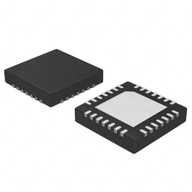
PDF Datasheet 数据手册内容提取
DATASHEET HI5960 FN4655 14-Bit, 130MSPS, High Speed D/A Converter Rev 6.00 March 31, 2005 The HI5960 is a 14-bit, 130MSPS (Mega Samples Per Features Second), high speed, low power, D/A converter which is • Throughput Rate . . . . . . . . . . . . . . . . . . . . . . . .130MSPS implemented in an advanced CMOS process. Operating from a single +3V to +5V supply, the converter provides • Low Power (at 100MSPS) at 5V . . . . . . . . . . . . . .175mW 20mA of full scale output current and includes edge- at 3V. . . . . . . . . . . . . . . .32mW triggered CMOS input data latches. Low glitch energy and • Adjustable Full Scale Output Current. . . . . 2mA to 20mA excellent frequency domain performance are achieved using a segmented current source architecture. • Internal 1.2V Bandgap Voltage Reference This device complements the HI5x60 and HI5x28 family of • Single Power Supply from +5V to +3V high speed converters, which includes 8, 10, 12, and 14-bit • Power Down Mode devices. • CMOS Compatible Inputs Ordering Information • Excellent Spurious Free Dynamic Range (77dBc, fS = 50MSPS, fOUT = 2.51MHz) TEMP. PART RANGE PKG. CLOCK • Excellent Multitone Intermodulation Distortion NUMBER (oC) PACKAGE DWG. # SPEED • Pb-Free Available (RoHS Compliant) HI5960IB -40 to 85 28 Ld SOIC M28.3 130MHz Applications HI5960IBZ -40 to 85 28 Ld SOIC M28.3 130MHz (See Note) (Pb-free) • Cellular Basestations HI5960IA -40 to 85 28 Ld TSSOP M28.173 130MHz • WLL, Basestation and Subscriber Units HI5960IAZ -40 to 85 28 Ld TSSOP M28.173 130MHz (See Note) (Pb-free) • Medical/Test Instrumentation HI5960IA-T -40 to 85 28 Ld TSSOP M28.173 130MHz • Wireless Communications Systems Tape and Reel • Direct Digital Frequency Synthesis HI5960IAZ-T -40 to 85 28 Ld TSSOP M28.173 130MHz • High Resolution Imaging Systems (See Note) Tape and Reel (Pb-free) • Arbitrary Waveform Generators HI5960SOICEVAL1 25 Evaluation Platform 130MHz Pinout NOTE: Intersil Pb-free products employ special Pb-free material sets; molding compounds/die attach materials and 100% matte tin plate HI5960 (SOIC, TSSOP) termination finish, which are RoHS compliant and compatible with TOP VIEW both SnPb and Pb-free soldering operations. Intersil Pb-free products are MSL classified at Pb-free peak reflow temperatures that meet or D13 (MSB) 1 28 CLK exceed the Pb-free requirements of IPC/JEDEC J STD-020. D12 2 27 DVDD D11 3 26 DCOM D10 4 25 ACOM D9 5 24 AVDD D8 6 23 COMP2 D7 7 22 IOUTA D6 8 21 IOUTB D5 9 20 ACOM D4 10 19 COMP1 D3 11 18 FSADJ D2 12 17 REFIO D1 13 16 REFLO D0 (LSB) 14 15 SLEEP FN4655 Rev 6.00 Page 1 of 12 March 31, 2005
HI5960 Typical Applications Circuit HI5960 D13 D13 (1) (25) ACOM D12 D12 (2) (15) SLEEP ACOM (16) REFLO D11 D11 (3) D10 D10 (4) (17) REFIO DCOM D9 D9 (5) 0.1F D8 D8 (6) D7 D7 (7) (18) FSADJ D6 D6 (8) RSET 1.91k D5 D5 (9) (22) IOUTA D/A OUT D4 D4 (10) 50 D3 D3 (11) D2 D2 (12) 50 D1 D1 (13) (21) IOUTB D/A OUT D0 D0 (LSB) (14) (23) COMP2 CLK (28) (19) COMP1 0.1F 50 DCOM (26) (20) ACOM 0.1F FERRITE BEAD BEAD + 10H DVDD (27) (24) AVDD 10H + +5V OR +3V (VDD) 10F 0.1F 0.1F 10F Functional Block Diagram IOUTA IOUTB (LSB) D0 CASCODE D1 CURRENT D2 SOURCE D3 D4 LATCH 9 LSBs D5 40 SWITCH 40 + D6 LATCH MATRIX SE3G1 MM ESNBTS D7 D8 D9 D10 UPPER 31 D11 5-BIT D12 DECODER (MSB) D13 COMP2 COMP1 CLK INT/EXT INT/EXT BIAS VOLTAGE GENERATION REFERENCE REFERENCE SELECT AVDD ACOM DVDD DCOM REFLO REFIO FSADJ SLEEP FN4655 Rev 6.00 Page 2 of 12 March 31, 2005
HI5960 Pin Descriptions PIN NO. PIN NAME DESCRIPTION 1-14 D13 (MSB) Through Digital Data Bit 13, (Most Significant Bit) through Digital Data Bit 0, (Least Significant Bit). D0 (LSB) 15 SLEEP Control Pin for Power-Down mode. Sleep Mode is active high; Connect to ground for Normal Mode. Sleep pin has internal 20A active pulldown current. 16 REFLO Connect to analog ground to enable internal 1.2V reference or connect to AVDD to disable internal reference. 17 REFIO Reference voltage input if internal reference is disabled. Reference voltage output if internal reference is enabled. Use 0.F cap to ground when internal reference is enabled. 18 FSADJ Full Scale Current Adjust. Use a resistor to ground to adjust full scale output current. Full Scale Output Current = 32 x VFSADJ/RSET. 19 COMP1 For use in reducing bandwidth/noise. Recommended: connect 0.1F to AVDD. 21 IOUTB The complimentary current output of the device. Full scale output current is achieved when all input bits are set to binary 0. 22 IOUTA Current output of the device. Full scale output current is achieved when all input bits are set to binary 1. 23 COMP2 Connect 0.1F capacitor to ACOM. 24 AVDD Analog Supply (+3V to +5V). 20, 25 ACOM Connect to Analog Ground. 26 DCOM Connect to Digital Ground. 27 DVDD Digital Supply (+3V to +5V). 28 CLK Clock Input. Input data to the DAC passes through the “master” latches when the clock is low and is latched into the “master” latches when the clock is high. Data presented to the “slave” latch passes through when the clock is logic high and is latched into the “slave” latches when the clock is logic low. Adequate setup time must be allowed for the MSBs to pass through the thermometer decoder before the clock goes high. This master-slave arrangement comprises an edge-triggered flip-flop, with the DAC being updated on the rising clock edge. It is recommended that the clock edge be skewed such that setup time is larger than the hold time. FN4655 Rev 6.00 Page 3 of 12 March 31, 2005
HI5960 Absolute Maximum Ratings Thermal Information Digital Supply Voltage DVDD to DCOM . . . . . . . . . . . . . . . . . +5.5V Thermal Resistance (Typical, Note 1) JA(oC/W) Analog Supply Voltage AVDD to ACOM. . . . . . . . . . . . . . . . . . +5.5V SOIC Package. . . . . . . . . . . . . . . . . . . . . . . . . . . . . 75 Grounds, ACOM TO DCOM . . . . . . . . . . . . . . . . . . . -0.3V to +0.3V TSSOP Package . . . . . . . . . . . . . . . . . . . . . . . . . . . 110 Digital Input Voltages (D9-D0, CLK, SLEEP). . . . . . . . DVDD + 0.3V Maximum Junction Temperature . . . . . . . . . . . . . . . . . . . . . . .150oC Reference Input Voltage Range. . . . . . . . . . . . . . . . . . AVDD + 0.3V Maximum Storage Temperature Range. . . . . . . . . . -65oC to 150oC Analog Output Current (IOUT) . . . . . . . . . . . . . . . . . . . . . . . . . 24mA Maximum Lead Temperature (Soldering 10s) . . . . . . . . . . . . .300oC (SOIC - Lead Tips Only) Operating Conditions HI5960IX . . . . . . . . . . . . . . . . . . . . . . . . . . . . . . . . . . -40oC to 85oC CAUTION: Stresses above those listed in “Absolute Maximum Ratings” may cause permanent damage to the device. This is a stress only rating and operation of the device at these or any other conditions above those indicated in the operational sections of this specification is not implied. NOTE: 1. JA is measured with the component mounted on an evaluation PC board in free air. Electrical Specifications AVDD = DVDD = +5V, VREF = Internal 1.2V, IOUTFS = 20mA, TA = 25oC for All Typical Values PARAMETER TEST CONDITIONS MIN TYP MAX UNITS SYSTEM PERFORMANCE Resolution 14 - - Bits Integral Linearity Error, INL “Best Fit” Straight Line (Note 8) -5 2.5 +5 LSB Differential Linearity Error, DNL (Note 8) -3 1.5 +3 LSB Offset Error, IOS (Note 8) -0.025 +0.025 % FSR Offset Drift Coefficient (Note 8) - 0.1 - ppm FSR/o Full Scale Gain Error, FSE With External Reference (Notes 2, 8) -10 2 +10 % FSR With Internal Reference (Notes 2, 8) -10 1 +10 % FSR Full Scale Gain Drift With External Reference (Note 8) - 50 - ppm FSR/ With Internal Reference (Note 8) - 100 - ppm FSR/ Full Scale Output Current, IFS 2 - 20 mA Output Voltage Compliance Range (Note 3, 8) -0.3 - 1.25 V DYNAMIC CHARACTERISTICS Maximum Clock Rate, fCLK (Note 3) 130 - - MHz Output Settling Time, (tSETT) 0.05% (8 LSB) (Note 8) - 35 - ns Singlet Glitch Area (Peak Glitch) RL = 25(Note 8) - 5 - pV•s Output Rise Time Full Scale Step - 2.5 - ns Output Fall Time Full Scale Step - 2.5 - ns Output Capacitance - 10 - pF Output Noise IOUTFS = 20mA - 50 - pA/Hz IOUTFS = 2mA - 30 - pA/Hz AC CHARACTERISTICS +5V Power Supply fCLK = 100MSPS, fOUT = 20.2MHz, 30MHz Span (Notes 4, 8) - 77 - dBc Spurious Free Dynamic Range, SFDR Within a Window fCLK = 100MSPS, fOUT = 5.04MHz, 8MHz Span (Notes 4, 8) - 97 - dBc fCLK = 50MSPS, fOUT = 5.02MHz, 8MHz Span (Notes 4, 8) - 97 - dBc FN4655 Rev 6.00 Page 4 of 12 March 31, 2005
HI5960 Electrical Specifications AVDD = DVDD = +5V, VREF = Internal 1.2V, IOUTFS = 20mA, TA = 25oC for All Typical Values (Continued) PARAMETER TEST CONDITIONS MIN TYP MAX UNITS +5V Power Supply fCLK = 100MSPS, fOUT = 4.0MHz (Notes 4, 8) - -71 - dBc Total Harmonic Distortion (THD) to Nyquist fCLK = 50MSPS, fOUT = 2.0MHz (Notes 4, 8) - -75 - dBc fCLK = 25MSPS, fOUT = 1.0MHz (Notes 4, 8) - -77 - dBc +5V Power Supply fCLK = 130MSPS, fOUT = 40.4MHz (Notes 4, 8) - 56 - dBc Spurious Free Dynamic Range, SFDR to Nyquist (fCLK/2) fCLK = 130MSPS, fOUT = 10.1MHz (Notes 4, 8) - 67 - dBc fCLK = 130MSPS, fOUT = 5.02MHz, T = 25oC (Notes 4, 8) 68 74 - dBc fCLK = 130MSPS, fOUT = 5.02MHz, T = Min to Max (Notes 4, 8) 66 - - dBc fCLK = 100MSPS, fOUT = 40.4MHz (Notes 4, 8) - 55 - dBc fCLK = 100MSPS, fOUT = 20.2MHz (Notes 4, 8) - 63 - dBc fCLK = 100MSPS, fOUT = 5.04MHz, T = 25oC (Notes 4, 8) 68 74 - dBc fCLK = 100MSPS, fOUT = 5.04MHz, T = Min to Max (Notes 4, 8) 66 - dBc fCLK = 100MSPS, fOUT = 2.51MHz (Notes 4, 8) - 76 - dBc fCLK = 50MSPS, fOUT = 20.2MHz (Notes 4, 8) - 65 - dBc fCLK = 50MSPS, fOUT = 5.02MHz, T = 25oC (Notes 4, 8) 68 74 - dBc fCLK = 50MSPS, fOUT = 5.02MHz, T = Min to Max (Notes 4, 8) 66 - - dBc fCLK = 50MSPS, fOUT = 2.51MHz (Notes 4, 8) - 77 - dBc fCLK = 50MSPS, fOUT = 1.00MHz (Notes 4, 8) - 79 - dBc fCLK = 25MSPS, fOUT = 1.0MHz (Notes 4, 8) - 79 - dBc +5V Power Supply fCLK = 20MSPS, fOUT = 2.0MHz to 2.99MHz, 8 Tones at 110kHz - 76 - dBc Multitone Power Ratio Spacing (Notes 4, 8) fCLK = 100MSPS, fOUT = 10MHz to 14.95MHz, 8 Tones at 530kHz - 76 - dBc Spacing (Notes 4, 8) +3V Power Supply fCLK = 100MSPS, fOUT = 20.2MHz, 30MHz Span (Notes 4, 8) - 80 - dBc Spurious Free Dynamic Range, SFDR Within a Window fCLK = 100MSPS, fOUT = 5.04MHz, 8MHz Span (Notes 4, 8) - 95 - dBc fCLK = 50MSPS, fOUT = 5.02MHz, 8MHz Span (Notes 4, 8) - 95 - dBc +3V Power Supply fCLK = 100MSPS, fOUT = 4.0MHz (Notes 4, 8) - -70 - dBc Total Harmonic Distortion (THD) to Nyquist fCLK = 50MSPS, fOUT = 2.0MHz (Notes 4, 8) - -74 - dBc fCLK = 25MSPS, fOUT = 1.0MHz (Notes 4, 8) - -76 - dBc FN4655 Rev 6.00 Page 5 of 12 March 31, 2005
HI5960 Electrical Specifications AVDD = DVDD = +5V, VREF = Internal 1.2V, IOUTFS = 20mA, TA = 25oC for All Typical Values (Continued) PARAMETER TEST CONDITIONS MIN TYP MAX UNITS +3V Power Supply fCLK = 130MSPS, fOUT = 40.4MHz (Notes 4, 8) - 48 - dBc Spurious Free Dynamic Range, SFDR to Nyquist (fCLK/2) fCLK = 130MSPS, fOUT = 10.1MHz (Notes 4, 8) - 66 - dBc fCLK = 130MSPS, fOUT = 5.02MHz (Notes 4, 8) - 74 - dBc fCLK = 100MSPS, fOUT = 40.4MHz (Notes 4, 8) - 49 - dBc fCLK = 100MSPS, fOUT = 20.2MHz (Notes 4, 8) - 59 - dBc fCLK = 100MSPS, fOUT = 5.04MHz (Notes 4, 8) - 72 - dBc fCLK = 100MSPS, fOUT = 2.51MHz (Notes 4, 8) - 77 - dBc fCLK = 50MSPS, fOUT = 20.2MHz (Notes 4, 8) - 56 - dBc fCLK = 50MSPS, fOUT = 5.02MHz, T = 25oC (Notes 4, 8) 68 73 - dBc fCLK = 50MSPS, fOUT = 5.02MHz, T = Min to Max (Notes 4, 8) 66 - - dBc fCLK = 50MSPS, fOUT = 2.51MHz (Notes 4, 8) - 76 - dBc fCLK = 50MSPS, fOUT = 1.00MHz (Notes 4, 8) - 79 - dBc fCLK = 25MSPS, fOUT = 1.0MHz (Notes 4, 8) - 78 - dBc +3V Power Supply fCLK = 20MSPS, fOUT = 2.0MHz to 2.99MHz, 8 Tones at 110kHz - 75 - dBc Multitone Power Ratio Spacing (Notes 4, 8) fCLK = 100MSPS, fOUT = 10MHz to 14.95MHz, 8 Tones at 530kHz - 77 - dBc Spacing (Notes 4, 8) VOLTAGE REFERENCE Internal Reference Voltage, VFSADJ Pin 18 Voltage with Internal Reference 1.13 1.2 1.28 V Internal Reference Voltage Drift - 60 - ppm Internal Reference Output Current - 50 - A Sink/Source Capability Reference Input Impedance - 1 - M Reference Input Multiplying Bandwidth (Note 8) - 1.4 - MHz DIGITAL INPUTS D11-D0, CLK Input Logic High Voltage with (Note 3) 3.5 5 - V 5V Supply, VIH Input Logic High Voltage with (Note 3) 2.1 3 - V 3V Supply, VIH Input Logic Low Voltage with (Note 3) - 0 1.3 V 5V Supply, VIL Input Logic Low Voltage with (Note 3) - 0 0.9 V 3V Supply, VIL Sleep Input Current, IIH -25 - +25 A Input Logic Current, IIH -20 - +20 A Input Logic Current, IIL -10 - +10 A Digital Input Capacitance, CIN - 5 - pF TIMING CHARACTERISTICS Data Setup Time, tSU See Figure 4 (Note 3) - 1.5 - ns Data Hold Time, tHLD See Figure 4 (Note 3) - 1.2 - ns Propagation Delay Time, tPD See Figure 4 - 2.5 - ns CLK Pulse Width, tPW1, tPW2 See Figure 4 (Note 3) 4 - - ns FN4655 Rev 6.00 Page 6 of 12 March 31, 2005
HI5960 Electrical Specifications AVDD = DVDD = +5V, VREF = Internal 1.2V, IOUTFS = 20mA, TA = 25oC for All Typical Values (Continued) PARAMETER TEST CONDITIONS MIN TYP MAX UNITS POWER SUPPLY CHARACTERISTICS AVDD Power Supply (Notes 9) 2.7 5.0 5.5 V DVDD Power Supply (Notes 9) 2.7 5.0 5.5 V Analog Supply Current (IAVDD) 5V or 3V, IOUTFS = 20mA - 23 - mA 5V or 3V, IOUTFS = 2mA - 5 - mA Digital Supply Current (IDVDD) 5V (Note 5) - 7 - mA 5V (Note 6) - 13 - mA 5V (Note 7) - 10 - mA 3V (Note 5) - 2 - mA 3V (Note 6) - 6 - mA 3V (Note 7) - 5 - mA Supply Current (IAVDD) Sleep Mode 5V or 3V, IOUTFS = Don’t Care - 2.7 - mA Power Dissipation 5V, IOUTFS = 20mA (Note 5) - 150 - mW 5V, IOUTFS = 20mA (Note 6) - 180 200 mW 5V, IOUTFS = 20mA (Note 7) - 165 - mW 5V, IOUTFS = 2mA (Note 6) - 80 - mW 3V, IOUTFS = 20mA (Note 5) - 75 - mW 3V, IOUTFS = 20mA (Note 6) - 87 100 mW 3V, IOUTFS = 20mA (Note 7) - 84 - mW 3V, IOUTFS = 2mA (Note 6) - 32 - mW Power Supply Rejection Single Supply (Note 8) -0.2 - +0.2 % FSR/V NOTES: 2. Gain Error measured as the error in the ratio between the full scale output current and the current through RSET (typically 625A). Ideally the ratio should be 32. 3. Parameter guaranteed by design or characterization and not production tested. 4. Spectral measurements made with differential transformer coupled output and no external filtering. 5. Measured with the clock at 50MSPS and the output frequency at 10MHz. 6. Measured with the clock at 100MSPS and the output frequency at 40MHz. 7. Measured with the clock at 130MSPS and the output frequency at 10MHz. 8. See “Definition of Specifications”. 9. It is recommended that the output current be reduced to 12mA or less to maintain optimum performance for operation below 3V. DVDD and AVDD do not have to be equal. FN4655 Rev 6.00 Page 7 of 12 March 31, 2005
HI5960 Definition of Specifications by using a sinusoidal waveform as the external reference with the digital inputs set to all 1s. The frequency is increased until Differential Linearity Error, DNL, is the measure of the step the amplitude of the output waveform is 0.707 (-3dB) of its size output deviation from code to code. Ideally the step size original value. should be 1 LSB. A DNL specification of 1 LSB or less guarantees monotonicity. Singlet Glitch Area, is the switching transient appearing on the output during a code transition. It is measured as the area Full Scale Gain Drift, is measured by setting the data inputs to under the overshoot portion of the curve and is expressed as a be all logic high (all 1s) and measuring the output voltage Volt-Time specification. This is tested using a single code through a known resistance as the temperature is varied from transition across a major current source. TMIN to TMAX. It is defined as the maximum deviation from the value measured at room temperature to the value measured at Spurious Free Dynamic Range, SFDR, is the amplitude either TMIN or TMAX. The units are ppm of FSR (full scale difference from the fundamental signal to the largest range) per oC. harmonically or non-harmonically related spur within the specified frequency window. Full Scale Gain Error, is the error from an ideal ratio of 32 between the output current and the full scale adjust current Total Harmonic Distortion, THD, is the ratio of the RMS value (through RSET). of the fundamental output signal to the RMS sum of the first five harmonic components. Integral Linearity Error, INL, is the measure of the worst case point that deviates from a best fit straight line of data values Detailed Description along the transfer curve. The HI5960 is a 14-bit, current out, CMOS, digital to analog Internal Reference Voltage Drift, is defined as the maximum converter. Its maximum update rate is 130MSPS and can be deviation from the value measured at room temperature to the powered by either single or dual power supplies in the value measured at either TMIN or TMAX. The units are ppm per recommended range of +3V to +5V. Operation with clock rates oC. higher than 130MSPS is possible; please contact the factory for more information. It consumes less than 180mW of power Offset Drift, is measured by setting the data inputs to all logic when using a +5V supply with the data switching at 130MSPS. low (all 0s) and measuring the output voltage through a known The architecture is based on a segmented current source resistance as the temperature is varied from TMIN to TMAX. It arrangement that reduces glitch by reducing the amount of is defined as the maximum deviation from the value measured current switching at any one time. In previous architectures at room temperature to the value measured at either TMIN or that contained all binary weighted current sources or a binary TMAX. The units are ppm of FSR (full scale range) per degree oC. weighted resistor ladder, the converter might have a substantially larger amount of current turning on and off at Offset Error, is measured by setting the data inputs to all logic certain, worst-case transition points such as midscale and low (all 0s) and measuring the output voltage through a known quarter scale transitions. By greatly reducing the amount of resistance. Offset error is defined as the maximum deviation of current switching at certain “major” transitions, the overall the output current from a value of 0mA. glitch of the converter is dramatically reduced, improving settling time, transient problems, and accuracy. Output Settling Time, is the time required for the output voltage to settle to within a specified error band measured from Digital Inputs and Termination the beginning of the output transition. The measurement is The HI5960 digital inputs are guaranteed to CMOS levels. done by switching quarter scale. Termination impedance was However, TTL compatibility can be achieved by lowering the 25 due to the parallel resistance of the 50 loading on the supply voltage to 3V due to the digital threshold of the input output and the oscilloscope’s 50 input. This also aids the buffer being approximately half of the supply voltage. The ability to resolve the specified error band without overdriving internal register is updated on the rising edge of the clock. To the oscilloscope. minimize reflections, proper termination should be Output Voltage Compliance Range, is the voltage limit implemented. If the lines driving the clock and the digital inputs imposed on the output. The output impedance should be are long 50 lines, then 50 termination resistors should be chosen such that the voltage developed does not violate the placed as close to the converter inputs as possible connected compliance range. to the digital ground plane (if separate grounds are used). These termination resistors are not likely needed as long as Power Supply Rejection, is measured using a single power the digital waveform source is within a few inches of the DAC. supply. The supply’s nominal +5V is varied 10% and the change in the DAC full scale output is noted. Ground Planes Reference Input Multiplying Bandwidth, is defined as the Separate digital and analog ground planes should be used. All 3dB bandwidth of the voltage reference input. It is measured of the digital functions of the device and their corresponding components should be located over the digital ground plane FN4655 Rev 6.00 Page 8 of 12 March 31, 2005
HI5960 and terminated to the digital ground plane. The same is true for known line impedance is to be driven, then the output load the analog components and the analog ground plane. Consult resistor should be chosen to match this impedance. The output Application Note 9853. voltage equation is: Noise Reduction VOUT = IOUT X RLOAD. To minimize power supply noise, 0.1F capacitors should be These outputs can be used in a differential-to-single-ended placed as close as possible to the converter’s power supply arrangement to achieve better harmonic rejection. The SFDR pins, AVDD and DVDD. Also, the layout should be designed measurements in this data sheet were performed with a 1:1 using separate digital and analog ground planes and these transformer on the output of the DAC (see Figure 1). With the capacitors should be terminated to the digital ground for DVDD center tap grounded, the output swing of pins 21 and 22 will be and to the analog ground for AVDD. Additional filtering of the biased at zero volts. The loading as shown in Figure 1 will power supplies on the board is recommended. result in a 500mV signal at the output of the transformer if the Voltage Reference full scale output current of the DAC is set to 20mA. The internal voltage reference of the device has a nominal value REQ IS THE IMPEDANCE of +1.2V with a 60ppm/oC drift coefficient over the full LOADING EACH OUTPUT temperature range of the converter. It is recommended that a 50 VOUT = (2 x IOUT x REQ)V 0.1F capacitor be placed as close as possible to the REFIO IOUTB PIN 21 pin, connected to the analog ground. The REFLO pin (16) 100 50 PIN 22 selects the reference. The internal reference can be selected if IOUTA pin 16 is tied low (ground). If an external reference is desired, HI5960 50 then pin 16 should be tied high (the analog supply voltage) and the external reference driven into REFIO, pin 17. The full scale 50REPRESENTS THE output current of the converter is a function of the voltage SPECTRUM ANALYZER reference used and the value of RSET. IOUT should be within FIGURE 1. the 2mA to 20mA range, though operation below 2mA is possible, with performance degradation. VOUT = 2 x IOUT x REQ, where REQ is ~12.5. Allowing the center tap to float will result in identical transformer output, If the internal reference is used, VFSADJ will equal however the output pins of the DAC will have positive DC approximately 1.2V (pin 18). If an external reference is used, offset. Since the DAC’s output voltage compliance range is - VFSADJ will equal the external reference. The calculation for 0.3V to +1.25V, the center tap may need to be left floating or IOUT (Full Scale) is: DC offset in order to increase the amount of signal swing IOUT(Full Scale) = (VFSADJ/RSET) X 32. available. The 50 load on the output of the transformer represents the spectrum analyzer’s input impedance. If the full scale output current is set to 20mA by using the internal voltage reference (1.2V) and a 1.91k RSET resistor, then the input coding to output current will resemble the following: TABLE 1. INPUT CODING vs OUTPUT CURRENT INPUT CODE (D13-D0) IOUTA (mA) IOUTB (mA) 1111 11111 11111 20 0 1000 00000 00000 10 10 0000 00000 00000 0 20 Outputs IOUTA and IOUTB are complementary current outputs. The sum of the two currents is always equal to the full scale output current minus one LSB. If single ended use is desired, a load resistor can be used to convert the output current to a voltage. It is recommended that the unused output be either grounded or equally terminated. The voltage developed at the output must not violate the output voltage compliance range of -0.3V to 1.25V. RLOAD (the impedance loading each current output) should be chosen so that the desired output voltage is produced in conjunction with the output full scale current. If a FN4655 Rev 6.00 Page 9 of 12 March 31, 2005
HI5960 Timing Diagrams CLK 50% D13-D0 V GLITCH AREA = 1/2 (H x W) ERROR BAND HEIGHT (H) IOUT WIDTH (W) t(ps) tSETT tPD FIGURE 2. OUTPUT SETTLING TIME DIAGRAM FIGURE 3. PEAK GLITCH AREA (SINGLET) MEASUREMENT METHOD tPW1 tPW2 50% CLK tSU tSU tSU tHLD tHLD tHLD D13-D0 tPD tSETT IOUT tPD tSETT tPD tSETT FIGURE 4. PROPAGATION DELAY, SETUP TIME, HOLD TIME AND MINIMUM PULSE WIDTH DIAGRAM FN4655 Rev 6.00 Page 10 of 12 March 31, 2005
HI5960 Small Outline Plastic Packages (SOIC) M28.3 (JEDEC MS-013-AE ISSUE C) N 28 LEAD WIDE BODY SMALL OUTLINE PLASTIC PACKAGE INDEX AREA H 0.25(0.010) M B M INCHES MILLIMETERS E SYMBOL MIN MAX MIN MAX NOTES -B- A 0.0926 0.1043 2.35 2.65 - A1 0.0040 0.0118 0.10 0.30 - 1 2 3 L B 0.013 0.0200 0.33 0.51 9 SEATING PLANE C 0.0091 0.0125 0.23 0.32 - -A- D A h x 45o D 0.6969 0.7125 17.70 18.10 3 E 0.2914 0.2992 7.40 7.60 4 -C- e 0.05 BSC 1.27 BSC - H 0.394 0.419 10.00 10.65 - e A1 C h 0.01 0.029 0.25 0.75 5 B 0.10(0.004) L 0.016 0.050 0.40 1.27 6 0.25(0.010) M C A M B S N 28 28 7 0o 8o 0o 8o - NOTES: Rev. 0 12/93 1. Symbols are defined in the “MO Series Symbol List” in Section 2.2 of Publication Number 95. 2. Dimensioning and tolerancing per ANSI Y14.5M-1982. 3. Dimension “D” does not include mold flash, protrusions or gate burrs. Mold flash, protrusion and gate burrs shall not exceed 0.15mm (0.006 inch) per side. 4. Dimension “E” does not include interlead flash or protrusions. In- terlead flash and protrusions shall not exceed 0.25mm (0.010 inch) per side. 5. The chamfer on the body is optional. If it is not present, a visual index feature must be located within the crosshatched area. 6. “L” is the length of terminal for soldering to a substrate. 7. “N” is the number of terminal positions. 8. Terminal numbers are shown for reference only. 9. The lead width “B”, as measured 0.36mm (0.014 inch) or greater above the seating plane, shall not exceed a maximum value of 0.61mm (0.024 inch) 10. Controlling dimension: MILLIMETER. Converted inch dimen- sions are not necessarily exact. FN4655 Rev 6.00 Page 11 of 12 March 31, 2005
HI5960 Thin Shrink Small Outline Plastic Packages (TSSOP) M28.173 N 28 LEAD THIN SHRINK SMALL OUTLINE PLASTIC INDEX E 0.25(0.010) M B M PACKAGE AREA E1 INCHES MILLIMETERS GAUGE -B- PLANE SYMBOL MIN MAX MIN MAX NOTES A - 0.047 - 1.20 - 1 2 3 A1 0.002 0.006 0.05 0.15 - L 0.05(0.002) SEATING PLANE 0.25 A2 0.031 0.051 0.80 1.05 - 0.010 b 0.0075 0.0118 0.19 0.30 9 -A- D A c 0.0035 0.0079 0.09 0.20 - D 0.378 0.386 9.60 9.80 3 -C- E1 0.169 0.177 4.30 4.50 4 e A2 A1 e 0.026 BSC 0.65 BSC - c b 0.10(0.004) E 0.246 0.256 6.25 6.50 - 0.10(0.004) M C A M B S L 0.0177 0.0295 0.45 0.75 6 N 28 28 7 NOTES: 0o 8o 0o 8o - 1. These package dimensions are within allowable dimensions of Rev. 0 6/98 JEDEC MO-153-AE, Issue E. 2. Dimensioning and tolerancing per ANSI Y14.5M-1982. 3. Dimension “D” does not include mold flash, protrusions or gate burrs. Mold flash, protrusion and gate burrs shall not exceed 0.15mm (0.006 inch) per side. 4. Dimension “E1” does not include interlead flash or protrusions. Inter- lead flash and protrusions shall not exceed 0.15mm (0.006 inch) per side. 5. The chamfer on the body is optional. If it is not present, a visual index feature must be located within the crosshatched area. 6. “L” is the length of terminal for soldering to a substrate. 7. “N” is the number of terminal positions. 8. Terminal numbers are shown for reference only. 9. Dimension “b” does not include dambar protrusion. Allowable dambar protrusion shall be 0.08mm (0.003 inch) total in excess of “b” dimen- sion at maximum material condition. Minimum space between protru- sion and adjacent lead is 0.07mm (0.0027 inch). 10. Controlling dimension: MILLIMETER. Converted inch dimensions are not necessarily exact. (Angles in degrees) © Copyright Intersil Americas LLC 2003-2005. All Rights Reserved. All trademarks and registered trademarks are the property of their respective owners. For additional products, see www.intersil.com/en/products.html Intersil products are manufactured, assembled and tested utilizing ISO9001 quality systems as noted in the quality certifications found at www.intersil.com/en/support/qualandreliability.html Intersil products are sold by description only. Intersil may modify the circuit design and/or specifications of products at any time without notice, provided that such modification does not, in Intersil's sole judgment, affect the form, fit or function of the product. Accordingly, the reader is cautioned to verify that datasheets are current before placing orders. Information furnished by Intersil is believed to be accurate and reliable. However, no responsibility is assumed by Intersil or its subsidiaries for its use; nor for any infringements of patents or other rights of third parties which may result from its use. No license is granted by implication or otherwise under any patent or patent rights of Intersil or its subsidiaries. For information regarding Intersil Corporation and its products, see www.intersil.com FN4655 Rev 6.00 Page 12 of 12 March 31, 2005

 Datasheet下载

