ICGOO在线商城 > 光电元件 > 光纤 - 收发器模块 > HFBR-5911ALZ

 Datasheet下载
- 型号: HFBR-5911ALZ
- 制造商: Avago Technologies
- 库位|库存: xxxx|xxxx
- 要求:
| 数量阶梯 | 香港交货 | 国内含税 |
| +xxxx | $xxxx | ¥xxxx |
查看当月历史价格
查看今年历史价格
HFBR-5911ALZ产品简介:
ICGOO电子元器件商城为您提供HFBR-5911ALZ由Avago Technologies设计生产,在icgoo商城现货销售,并且可以通过原厂、代理商等渠道进行代购。 HFBR-5911ALZ价格参考。Avago TechnologiesHFBR-5911ALZ封装/规格:光纤 - 收发器模块, Fiber Optic Transceiver Module General Purpose 1.25Gbd 850nm 3.14V ~ 3.47V LC Duplex Pluggable, SFP。您可以下载HFBR-5911ALZ参考资料、Datasheet数据手册功能说明书,资料中有HFBR-5911ALZ 详细功能的应用电路图电压和使用方法及教程。
| 参数 | 数值 |
| 产品目录 | |
| 描述 | TXRX MMF GBE 1.25BGD EXT TEMP光纤发射器、接收器、收发器 1.25G MM 2X5 3.3V SF F/LC/ExTp RoHS |
| 产品分类 | 光纤 - 收发器光纤 |
| 品牌 | Avago Technologies US Inc. |
| 产品手册 | http://www.avagotech.com/pages/en/optical_transceivers/ethernet/gigabit_ethernet/hfbr-5911alz/ |
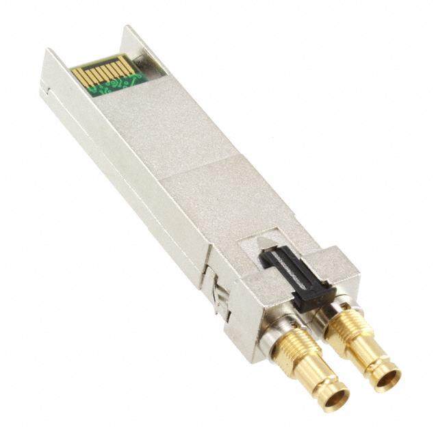
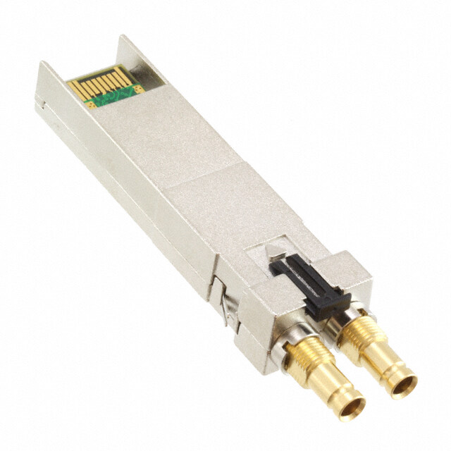
| 产品图片 |
|
| rohs | 符合RoHS无铅 / 符合限制有害物质指令(RoHS)规范要求 |
| 产品系列 | 光纤发射器、接收器、收发器,Avago Technologies HFBR-5911ALZ- |
| mouser_ship_limit | 该产品可能需要其他文件才能进口到中国。 |
| 数据手册 | http://www.avagotech.com/docs/AV01-0048EN |
| 产品型号 | HFBR-5911ALZ |
| 产品 | Transceivers |
| 产品种类 | 光纤发射器、接收器、收发器 |
| 其它名称 | 516-2419 |
| 商标 | Avago Technologies |
| 安装类型 | 可插入式,SFP |
| 封装 | Tray |
| 封装/箱体 | DIP-10 with Connector |
| 工作电源电压 | 3.3 V |
| 工厂包装数量 | 10 |
| 应用 | 通用 |
| 数据速率 | 1.25Gbd |
| 最大工作温度 | + 85 C |
| 最小工作温度 | - 10 C |
| 标准包装 | 10 |
| 波长 | 850nm |
| 电压-电源 | 3.14 V ~ 3.47 V |
| 纤维类型 | Multimode |
| 连接器类型 | LC 双工 |


- 商务部:美国ITC正式对集成电路等产品启动337调查
- 曝三星4nm工艺存在良率问题 高通将骁龙8 Gen1或转产台积电
- 太阳诱电将投资9.5亿元在常州建新厂生产MLCC 预计2023年完工
- 英特尔发布欧洲新工厂建设计划 深化IDM 2.0 战略
- 台积电先进制程称霸业界 有大客户加持明年业绩稳了
- 达到5530亿美元!SIA预计今年全球半导体销售额将创下新高
- 英特尔拟将自动驾驶子公司Mobileye上市 估值或超500亿美元
- 三星加码芯片和SET,合并消费电子和移动部门,撤换高东真等 CEO
- 三星电子宣布重大人事变动 还合并消费电子和移动部门
- 海关总署:前11个月进口集成电路产品价值2.52万亿元 增长14.8%


PDF Datasheet 数据手册内容提取
HFBR-5911LZ/ALZ Small Form Factor Optical Transceiver for Gigabit Ethernet (1.25 GBd) and iSCSI Data Sheet Description Features The HFBR-5911LZ/ALZ optical transceiver from Avago • IEEE 802.3 Gigabit Ethernet Technologies is designed for use in short-reach multi- (1.25 Gbd) 1000BASE-SX compliant mode fiber optic (1000BASE-SX) links between Gigabit • Industry standard small form factor (SFF) package Ethernet networking equipment. Interoperable with • LC-duplex connector optical interface all equipment meeting the Gigabit Ethernet industry • 850 nm Vertical cavity surface emitting laser standard, it is compliant with the Small Form Factor Multi • Internally terminated and ac coupled data IO Source Agreement and requires a 3.3 V dc power supply. • Extended operating temperature range (HFBR- The electrical interface follows the 2 x 5 format while the 5911ALZ only) : optical interface uses the LC-Duplex connector. -10 to +85 °C • Signal detect TTL Related Products • Maximum link lengths: • AFBR-5710LZ: 850 nm Small Form Factor Pluggable 62.5/125 µm fiber 275 m optical transceiver for short reach Gigabit Ethernet 50/125 µm fiber 550 m (1000BASE-SX) links • Laser AEL Class 1 (eye safe) per: • HDMP-1687: Quad SerDes IC for Gigabit Ethernet • US 21 CFR(J) with 10 bit parallel interface and TTL clock input • EN 60825-1 (+All) • HDMP-1685A: Quad SerDes IC for Gigabit Ethernet • +3.3 V dc power supply with 5 bit parallel interface and DDR TTL clock input • Manufactured in ISO 9001 facilities • HDMP-1636A/46A: Single SerDes IC for Gigabit Eth- • RoHS Compliant ernet and Fiber Channel Applications • HDMP-1637A: Single SerDes IC with PECL RefClk • Short-reach Gigabit Ethernet links • HDMP-1638: Single SerDes IC with PECL RefClk and • High speed backplane interconnects Dual Serial I/O • Switched backbones • HDMP-2634: Single SerDes IC 2.5/1.25 Gigabit • iSCSI applications
Overview Tx_Disable Avago Technologies’ HFBR-5911LZ/ALZ optical transceiver The HFBR-5911LZ/ALZ accepts a TTL transmit disable supports high-speed serial links over multimode optical control signal input which shuts down the transmitter. A fiber at signaling rates of up to 1.25 Gb/s. Compliant high signal implements this function while a low signal with the Small Form Factor (SFF) Multi Source Agreement allows normal transceiver operation. In the event of a (MSA) for 2 x 5 pin LC Duplex transceivers and IEEE 802.3 fault (e.g., eye safety circuit activated), cycling this control specification for Gigabit Ethernet (GbE) links (1000BASE- signal resets the module as depicted in Figure 5 page 12. SX), the part is interoperable and interchangeable with A pull-down resistor enables the laser if the line is not other conformant devices. Supported Gigabit Ethernet connected on the host board. link lengths are described in Table 1, but the transceiver Host systems should allow a 10 ms interval between suc- can also be used for other high-speed serial applications, cessive assertions of this control signal. such as iSCSI. Eye Safety Circuit The SFF package of the HFBR-5911LZ/ALZ allows design- ers of Gigabit Ethernet networking equipment to maxi- The HFBR-5911LZ/ALZ provides Class 1 eye safety by mize their use of available board space. The footprint design and has been tested for compliance with the of the HFBR-5911LZ/ALZ is significantly smaller than requirements listed in Table 11. The eye safety circuit those of other GbE transceivers formats - 25% smaller continuously monitors optical output power levels and than SFP cage assemblies, 30% smaller than traditional will disable the transmitter upon detecting an unsafe 1 x 9 transceivers and 70% smaller than GBIC rail as- condition. Such unsafe conditions can be due to inputs semblies. The HFBR-5911LZ/ALZ trace keep-out area is from the host board (VCC fluctuation, unbalanced code) less than 10% as large as that required by SFP transceiv- or faults within the transceiver. ers. For applications not requiring hot-pluggability, the HFBR-5911LZ/ALZ offers a more space-efficient package Receiver Section without the additional cost and complexity imposed by The receiver section includes the Receiver Optical Subassem- pluggable architecture. bly (ROSA) and the amplification/quantization circuitry. The ROSA, containing a PIN photodiode and custom transimped- Module Diagrams ance preamplifier, is located at the optical interface and mates The major functional components of the HFBR-5911LZ/ALZ with the LC optical connector. The ROSA output is fed to a are illustrated in Figure 2 page 9. The external configu- custom IC that provides post-amplification and quantization. ration of the transceiver is depicted in Figure 3 page 10 while the host board and front panel layouts defined by Signal Detect the SFF MSA are shown in Figure 4, page 11. The post-amplification/quantizer IC also includes transition detection circuitry that monitors the ac level of the incoming Transmitter Section optical signal and provides a TTL status signal to the host. An The transmitter section consists of the Transmitter Optical adequate optical input results in a high output while a low Subassembly (TOSA) and laser driver circuitry. The TOSA, Signal Detect output indicates an unusable optical input. The containing an 850 nm VCSEL (Vertical Cavity Surface Emit- Signal Detect thresholds are set so that a low output indicates ting Laser) light source, is located at the optical interface and a definite optical fault has occurred (e.g., disconnected or mates with the LC optical connector. The TOSA is driven by broken fiber connection to receiver, failed transmitter, etc.). a custom IC which uses the incoming differential PECL logic signals to modulate the laser diode drive current. This Tx laser driver circuit regulates the optical output power at a constant level provided that the incoming data pattern is dc balanced (8B10B code for example). 2
Electrical Interfaces EMI Immunity The HFBR-5911LZ/ALZ interfaces with the host circuit Due to its shielded design, the EMI immunity of the HFBR- board through the ten I/O pins identified by function in 5911LZ/ALZ exceeds typical industry standards. Table 4. These pins are sized for use in boards between Electromagnetic Interference (EMI) 0.062 in. and 0.100 in. thick. The board layout for this interface is depicted in Figure 4. Equipment incorporating Gigabit transceivers is typically sub- The HFBR-5911LZ/ALZ transmit and receive interfaces ject to regulation by the FCC in the United States, TUV in the require PECL differential signal lines on the host board. To European Union and VCCI in Japan. The HFBR-5911LZ/ALZ’ s simplify board requirements, transmitter bias resistors and compliance to these standards is detailed in Table 11. ac coupling capacitors are incorporated into the transceiver The metal housing and shielded design of the HFBR- module and so are not required on the host board. 5911LZ/ALZ minimize the EMI challenge facing the The Tx_Disable and Signal Detect lines require TTL lines on equipment designer. the host board if they are to be utilized. The transceiver will Flammability operate normally if these lines are not connected on the host board. The HFBR-5911LZ/ALZ optical transceiver is made of metal and high strength, heat resistant, chemical resistant and Figure 2 depicts a recommended interface circuit to link the UL 94V-0 flame retardant plastic. HFBR-5911LZ/ALZ to the supporting physical layer ICs. Timing for the MSA compliant control signals implement- Caution ed in this transceiver are listed in Table 9 and diagramed There are no user serviceable parts nor any maintenance in Figure 5. required for the HFBR-5911LZ/ALZ. All adjustments are made at the factory before shipment. Tampering with, PCB Assembly Process Compatibility modifying, misusing or improperly handling the HFBR- The HFBR-5911LZ/ALZ is compatible with industry- 5911LZ/ALZ will void the product warranty. It may also standard wave solder and aqueous wash processes as result in improper operation and possibly overstress the detailed in Table 10. The transceiver is shipped with a laser source. Performance degradation or device failure process plug to keep out impinging liquids, but is not may result. Connection of the HFBR-5911LZ/ALZ to a intended to be immersed. After assembly, the process light source not compliant to the Gigabit Ethernet speci- plug should be kept in place as a dust plug when the fication (IEEE 802.3), operating above the recommended transceiver is not in use. absolute maximum operating conditions or in a manner inconsistent with it’s design and function may result in Regulatory Compliance exposure to hazardous radiation and may constitute The HFBR-5911LZ/ALZ complies with all ap- an act of modifying or manufacturing a laser product. plicable laws and regulations as detailed in Person’s performing such an act are required by law to Table 11. Certification level is dependent of the overall recertify and re-identify the laser product under the pro- configuration of the host equipment. The transceiver visions of U.S. 21 CFR (Subchapter J). performance is offered as a figure of merit to assist the designer. Electrostatic Discharge (ESD) The HFBR-5911LZ/ALZ is compatible with ESD levels found in typical manufacturing and operating environments as de- scribed in Table 11. In the normal handling and operation of optical transceivers, ESD is of concern in two circumstances. The first case is during handling of the transceiver prior to soldering onto the host board. To protect the device, it’s important to use normal ESD handling precautions. These include using grounded wrist straps, workbenches and floor mats wherever the transceiver is handled. The second case to consider is static discharges to the exterior of the host equipment chassis after assembly. If the optical interface is exposed to the exterior of the host equipment cabinet, the transceiver may be subject to system-level ESD requirements. 3
Table 1 - Supported Links from IEEE 802.3 Link length Modal bandwidth @ 850 nm Fiber Type (min. overfilled launch) (MHz - km) Minimum Maximum Units 62.5 µm MMF 160 2 220 m 62.5 µm MMF 200 2 275 m 50 µm MMF 400 2 500 m 50 µm MMF 500 2 550 m Table 2 - Absolute Maximum Ratings The Absolute Maximum Ratings are those values beyond which damage to the device may occur if these limits are exceeded for other than a short period of time. See Reliability Data Sheet for specific reliability performance. Parameter Symbol Minimum Typical Maximum Units Reference Storage Temperature TS -40 +100 ° C Operating Temperature - Case TC -10 +85 ° C Aqueous Wash Pressure 110 psi Relative Humidity - non condensing RH 5 95 % Supply Voltage VCC -0.5 3.63 V Voltage to any pin -0.5 3.63 V TTL Transmit Disable Current II -3.0 3.0 mA Table 3 - Recommended Operating Conditions The Recommended Operating Conditions are those values outside of which device reliability and performance to data sheet are not implied, and damage to the device may occur over an extended period of time. See Reliability Data Sheet for specific reliabil- ity performance. Parameter Symbol Minimum Typical Maximum Units Reference Temperature - Case HFBR-5911LZ TC 0 +70 °C 11 HFBR-5911ALZ TC -10 +85 °C Supply Voltage VCC 3.14 3.47 V Input Data Differential Voltage 0.4 1.6 V TTL Transmit Disable Input Voltage - Low VIL 0.8 V TTL Transmit Disable Input Voltage - High VIH VCC-1.3 VCC V TTL Transmit Disable Input Current II -1.0 400 mA Notes: 1. Operating the transceiver beyond +70 °C for extended periods can adversely affect device reliability. 4
Table 4 - Pin Description Pin Symbol Functional Description Logic Reference MS MS Mounting Stud n/a 4 HL HL Housing Lead n/a 5 1 Veer Receiver Signal Ground n/a 2 Vccr Receiver Power Supply n/a 3 SD Signal Detect TTL 6 4 RD- Receiver Data Out Bar PECL 7 5 RD+ Receiver Data Out PECL 7 MS MS Mounting Stud n/a 4 HL HL Housing Lead n/a 5 6 Vcct Transmitter Power Supply n/a 7 Veet Transmitter Signal Ground n/a 8 TDis Transmitter Disable TTL 8 9 TD+ Transmitter Data In PECL 9 10 TD- Transmitter Data In Bar PECL 9 Figure 1 - Pin out drawing Table 5 - Transmitter Electrical Characteristics HFBR-5911LZ (T = 0ºC to +70ºC, V = 3.14 V to 3.47 V) C CC HFBR-5911ALZ (T = -10 °C to +85 °C, V = 3.14 V to 3.47 V) C CC Parameter Symbol Minimum Typical Maximum Units Reference Transmitter Supply Current ICCTx 55 75 mA Power Dissipation PDISS 180 260 mW Data Input Differential Voltage VIH-VIL 400 1600 mV Power Supply Noise Rejection PSNR 100 mVP-P 10 Notes: 4. The mounting studs provide mechanical attachment to the circuit board and connection to the equipment chassis ground. The MS via holes must not be tied to signal ground and may be tied to chassis ground. 5. The housing leads provide additional signal grounding. The HL via holes must be tied to signal ground. 6. Normal operation: Logic “1” output No-signal condition: Logic “0” output 7. AC coupled differential output. LVPECL signal. Interfacing ICs may require internal biasing. 8. Transmitter Output Disabled: (Vcct-1.3 V)<V<Vcct Transmitter Output Enabled: Veet < V < (Veet +0.8 V) 9. AC coupled differential input, no external termination required. 100 ohm internal termination provided. 10. Tested with a 100 mVP-P sinusoidal signal in the frequency range from 10 KHz to 2 MHz on the VCC supply with the recommended power sup- ply filter (with C8) in place. Typically, a change in sensitivity of less than 1 dB is experienced. 5
Table 6 - Transmitter Optical Characteristics HFBR-5911LZ (T = 0ºC to +70ºC, V = 3.14 V to 3.47 V) C CC HFBR-5911ALZ (T = -10 °C to +85 °C, V = 3.14 V to 3.47 V) C CC Parameter Symbol Minimum Typical Maximum Units Reference Optical Output Power 62.5 µm POUT -9.5 -1.5 dBm avg. 11 50 µm -9.5 -1.5 Tx_Disable Optical Output Power POUT DIS -30 dBm avg. 11 Optical Extinction Ratio ER 9 dB 12 Center Wavelength lC 830 850 860 nm Spectral Width - rms s 0.85 nm rms Optical Rise Time tr 0.26 ns 13 Optical Fall Time tf 0.26 ns 13 RIN12 -117 dB/Hz Coupled Power Ratio CPR 9 dB 14 Contributed Total Jitter TJ 2270.284 psUI 15 Table 7 - Receiver Electrical Characteristics HFBR-5911LZ (T = 0ºC to +70ºC, V = 3.14 V to 3.47 V) C CC HFBR-5911ALZ (T = -10 °C to +85 °C, V = 3.14 V to 3.47 V) C CC Parameter Symbol Minimum Typical Maximum Units Reference Receiver Supply Current ICCRX 135 mA Power Dissipation PDISS 230 470 mW Power Supply Noise Rejection PSNR 100 mVP-P 16 Data Output Differential Voltage VOH-VOL 0.4 1.3 V Data Output Rise Time tr 0.4 ns Data Output Fall Time tf 0.4 ns TTL Signal Detect Output Voltage - Low VOL 0.6 V TTL Signal Detect Output Voltage - High VOH 2.2 V Notes: 11. The maximum Optical Output Power complies with IEEE 802.3 and is Class 1 laser eye safe. 12. Optical Extinction Ratio is defined as the ratio of the average optical power of the transmitter in the high (“1”) state to the low (“0”) state. The transmitter is driven with a Gigabit Ethernet 1250 MBd 8b/10b encoded serial data pattern. Optical Extinction Ratio is expressed in decibels (dB) by the relationship 10log(Phigh avg/Plow avg). 13. Optical Rise and Fall Times are 20-80% value. Laser transmitter pulse characteristics are typically specified by an eye diagram - see Figure 6. The characteristics include rise time, fall time, pulse overshoot, pulse undershoot and ringing, all of which are controlled to prevent excessive degradation of receiver sensitivity. These parameters are specified by the referenced Gigabit Ethernet eye diagram using the required filter. The output optical waveform complies with the requirements of the eye mask described in IEEE 802.3 section 38.6.10 and Figure 38-2. 14. CPR is measured in accordance with EIA/TIA-526-14A as referenced in IEEE 802.3 section 38.6.10. 15. Measured at TP2. TP refers to the compliance point specified by IEEE 802.3, section 38.2.1. 16. Tested with a 100 mVP-P sinusoidal signal in the frequency range from 10 Hz to 2 MHz on the VCC supply with the recommended power sup- ply filter (with C8) in place. Typically, a change in sensitivity of less than 1 dB is experienced. 6
Table 8 - Receiver Optical Characteristics HFBR-5911LZ (T = 0ºC to +70ºC, V = 3.14 V to 3.47 V) C CC HFBR-5911ALZ (T = -10 °C to +85 °C, V = 3.14 V to 3.47 V) C CC Parameter Symbol Minimum Typical Maximum Units Reference Input Optical Power PIN -17 0 dBm avg. 17 Stressed Receiver Sensitivity -12.5-13.5 dBm avg. 18 62.5 µm 50 µm Contributed Total Jitter TJ 2660.332 psUI Receive Electrical 3dB Upper Cutoff Frequency 1500 MHz 19 Operating Center Wavelength lC 770 850 860 nm Return Loss RL 12 dB 20 Signal Detect Assert Power Level PA -17 dBm avg. 21 Signal Detect Deassert Power Level PD -30 dBm avg. 21 Signal Detect Hysteresis PA - PD 1.5 dB 21 Table 9 - Transceiver Timing Characteristics HFBR-5911LZ (T = 0ºC to +70ºC, V = 3.14 V to 3.47 V) C CC HFBR-5911ALZ (T = -10 °C to +85 °C, V = 3.14 V to 3.47 V) C CC Parameter Symbol Minimum Typical Maximum Units Reference Tx Disable Assert Time t_off 100 µs 22 Tx Disable Deassert Time t_on 1.0 ms 23 Time to initialize t_init 300 ms 24 Tx Disable Pulse Width to Reset t_reset 10 µs 25 Interval between Transmit Disable Assertions 10 ms Signal Detect Assert Time SD_on 100 µs 26 Signal Detect Deassert Time SD_off 350 µs 27 Table 10 - PCB Assembly Process Compatibility Parameter Symbol Minimum Typical Maximum Units Reference Hand Lead Soldering Temperature/Time TSOLD/tSOLD +260/10 ° C / sec Wave Soldering and Aqueous Wash TSOLD/tSOLD +260/10 ° C / sec Aqueous Wash Pressure 110 psi Notes: 17. Receiver sensitivity is measured using a worst case extinction ratio penalty while sampling at the center of the eye. 18. Stressed receiver sensitivity is measured using the conformance test signal defined by IEEE 802.3, section 38.6.11. The conformance test sig- nal is conditioned by applying deterministic jitter and intersymbol interference. 19. The Receive Electrical 3 dB Upper Cutoff Frequency of the receiver is measured using the technique outlined in IEEE 802.3, section 38.6.11. 20. Return Loss is defined as the minimum attenuation (dB) of received optical power for energy reflected back into the optical fiber. 21. With valid 8b/10b encoded data. 22. Time from rising edge of Tx_Disable to when modulated optical output falls below 10% of nominal. 23. Time from falling edge of Tx_Disable to when the modulated optical output rises above 90% of nominal. 24. Time from power on or falling edge of Tx_ Disable to when the modulated optical output rises above 90% of nominal. 25. Time Tx_Disable must be held high to disable transmitter. Measured from leading edge of Tx_Disable to when the modulated optical output falls below 10% of nominal. 26. Time from SD deassert to SD assert. 27. Time from non-SD assert to SD deassert. 7
Table 11- Regulatory Compliance Feature Test Method Criteria Electrostatic Discharge (ESD) MIL-STD-883C Class 1 compliance. Withstands >1500 V. to the Electrical Pins Method 3015.4 Electrostatic Discharge (ESD) Variation of IEC 61000-4-2 Typically withstands at least 25 kV without damage when to the Duplex LC Receptacle the duplex LC connector receptacle is contacted by a Hu- man Body Model probe. Fulfills Live Traffic ESD testing up to 8 kV with less than 1 errored second. Electromagnetic Interference FCC Class BCENELEC EN55022 Margins are dependent on customer board and Chassis (EMI) Class B (CISPR 22A) Class 1 design. Immunity Variation of IEC 6100-4-3 Typically shows no measurable effect from a 10 mV/m field swept from 80 to 1000 MHz applied to the transceiver with- out a chassis enclosure. Eye Safety US FDA CDRH AEL Class 1EN (IEC) CDRH certification # 9720151-24TUV file # E9971083.14UL 60825-1, 2,EN60950 Class 1 file # E173874 Component Recognition Underwriter’s Laboratories and UL file # E173874 Canadian Standards Association Joint Component Recognition for Information Technology Equip- ment Including Electrical Business Equipment RoHS Compliance Less than 1000 ppm of cadmium, lead, mercury, hexavalent chromium, polybrominated biphenyls, and polybrominated biphenyl ethers. 8
3.3 V dc + GND 7 V V 2 V 2 EET 9 50 W CC EE CLOCK LASER TD+ TD+ SYNTHESIS DRIVER PECL 100 W OUTPUT CIRCUIT CIRCUIT INPUT TD- 10 50 W TD- DRIVER PARALLEL TO SERIAL CIRCUIT TO TRANSMIT 8 LVTTL DISABLE STAGE 6 L1 V HFBR-5911LZ CCT C1 1 µH C7 TFRIBAENRS-COEPITVIECR 0.1 µF 0.1 µF 3.3 V dc SERIAHL/DDMEP-S-1E6R8I7ALIZER V 2 L2 +C10 (SERDES - 10 BIT CCR C2 C8* 1 µH C9 10 µF TRANSCEIVER) V CC 0.1 µF 10 µF 0.1 µF 1.8 kW SIGNAL DETECT SD 3 CIRCUIT TO LVTTL STAGE 130 W RD- 4 50 W RD- CLOCK RECOVERY PRE- POST- R14 INPUT CIRCUIT AMPLIFIER AMPLIFIER RD+ 5 50 W 100 W RD+ BUFFER SPEARRIAALLL TEOL 130 W V 1 CIRCUIT EER SEE HDMP-1687 DATA SHEET FOR DETAILS ABOUT THIS TRANSCEIVER IC. NOTES: USE SURFACE-MOUNT COMPONENTS FOR OPTIMUM HIGH-FREQUENCY PERFORMANCE. USE 50 W MICROSTRIP OR STRIPLINE FOR SIGNAL PATHS. LOCATE 50 W TERMINATIONS AT THE INPUTS OF RECEIVING UNITS. *C8 IS A RECOMMENDED BYPASS CAPACITOR FOR ADDITIONAL LOW FREQUENCY NOISE FILTERING. THE SIGNAL DETECT OUTPUT ON THE HFBR-5911LZ CONTAINS AN INTERNAL 1.8 kW PULL UP RESISTOR. THE OUTPUT STAGE ON THE HFBR5911L IS A PUSH PULL CONFIGURATION AND THEREFORE DOES NOT REQUIRE AN EXTERNAL PULL UP RESISTOR. Figure 2 - Recommended Gigabit/sec Ethernet HFBR-5911LZ/ALZ Fiber-Optic Transceiver and HDMP-1687 SERDES Integrated Circuit Transceiver Interface and Power Supply Filter Circuits. 9
AVAGO HFBR-5911LZ 850 nm LASER PROD 21CFR(J) CLASS 1 COUNTRY OF ORIGIN YYWW XXXXXXXX 13.59 15.05 MAX. UNCOMPRESSED (.535) (.593) 48.19 SEE DETAIL 1 (1.897) 6.25 (.246) 13.14 11.30 UNCOMPRESSED (.517) (.445) TX RX 9.80 8.89 MAX. (0.386) (.350) 1.00 4 x (.039) 14.68 10.16 (1.400.106) (.21.1952)MIN. 7.11 (.578) (.400) (.280) 13.34 4.57 (.525) (.180) 28.45 (1.120) 1.07 Tcase REFERENCE POINT 0.46 2 x Ø 10 x (.042) (.018) 5.72 (.225) 10.16 6 7 8 9 10 11.84 (.400) (.466) 5 4 3 2 1 13.76 4 x 1.78 (.542) (.070) 17.79 AREA FOR PROCESS PLUG (.700) DETAIL 1 19.59 SCALE 3 x (.771) ALL DIMENSIONS IN MILLIMETERS (INCHES) Figure 3 - External Configuration 10
0.81 ± .10 20 x Ø (.032 ± .004) SEE DETAIL B SEE NOTE 3 1.40 ± .10 25.75 4 x Ø(.055 ± .004) (NOTE 5) (1.014) SEE DETAIL A 13.34 12.16 15.24 (.525) (.479) MIN. PITCH (.600) 5 4 3 2 1 7.59 10.16 (.299) (.400) 6 7 8 9 10 2.29 2 x Ø MAX. (AREA FOR EYELET'S) (.090) 1.40 ± .10 4.57 2 x Ø (NOTE 4) (.055 ± .004) (.180) 3 7.11 (.118) (.280) 3.56 3 (.140) 8.89 (.118) (.350) 6 (.236) 1.78 9 X (.070) DETAIL A (3 x) 1.8 .071 1 .039 15.24 MIN. PITCH (.600) + 1.50 DETAIL B (4 x) 1.00 - 0 14.22 ± .10 (+.059) (.039) A (.560 ± .004) (- .000) TOP OF PCB A 10.16 ± .10 (.400 ± .004) + 0 A SECTION A - A 15.75 - 0.75 (+.000) (.620) (- .030) NOTES: 1. THIS PAGE DESCRIBES THE RECOMMENDED CIRCUIT BOARD LAYOUT AND FRONT PANEL OPENINGS FOR SFF TRANSCEIVERS. 2. THE HATCHED AREAS ARE KEEP-OUT AREAS RESERVED FOR HOUSING STANDOFFS. NO METAL TRACES ALLOWED IN KEEP-OUT AREAS. 3. THIS DRAWING SHOWS EXTRA PIN HOLES FOR 2 x 6 PIN AND 2 x 10 PIN TRANSCEIVERS. THESE EXTRA HOLES ARE NOT REQUIRED FOR HFBR-5911LZ AND OTHER 2 x 5 PIN SFF MODULES. 4. HOLES FOR MOUNTING STUDS MUST NOT BE TIED TO SIGNAL GROUND BUT MAY BE TIED TO CHASSIS GROUND. 5. HOLES FOR HOUSING LEADS MUST BE TIED TO SIGNAl GROUND. 6. ALL DIMENSIONS ARE IN MILLIMETERS (INCHES). Figure 4 - Recommended host board layout (from SFF MSA) 11
V > 3.15 V V > 3.15 V CC CC TX_FAULT TX_FAULT TX_DISABLE TX_DISABLE Transmitted Signal Transmitted Signal t_init t_init TX_FAULT Occurrence of Fault TX_FAULT TX_DISABLE TX_DISABLE Transmitted Signal Transmitted Signal t_fault t_reset t_off t_on t_init *SFP shall clear TX_FAULT in <t_init if the failure is transient Figure 5 - Transceiver timing diagrams NORMALIZED TIME (UNIT INTERVAL) 0 0.22 0.375 0.625 0.78 1.0 130 1.30 %) 100 1.00 E E ( UD D T U 80 0.80 LI T P LI M AMP 50 0.50 ED A ED LIZ Z A LI M MA 20 0.20 OR R N O N 0 0.0 -20 -0.20 0 22 37.5 62.5 78 100 NORMALIZED TIME (% OF UNIT INTERVAL) Figure 6 - Gigabit Ethernet Transmitter eye mask diagram Ordering Information The HFBR-5911LZ/ALZ is available for production orders through the Avago Technologies Component Field Sales Of- fices and Authorized Distributors world wide. Temperature ranges 0 °C to +70 °C - HFBR-5911LZ -10 °C to +85 °C - HFBR-5911ALZ For product information and a complete list of distributors, please go to our web site: www.avagotech.com Avago, Avago Technologies, and the A logo are trademarks of Avago Technologies in the United States and other countries. Data subject to change. Copyright © 2005-2013 Avago Technologies. All rights reserved. AV01-0048EN - July 11, 2013