ICGOO在线商城 > 集成电路(IC) > 时钟/计时 - 可编程计时器和振荡器 > HEF4541BT,512

 Datasheet下载
- 型号: HEF4541BT,512
- 制造商: NXP Semiconductors
- 库位|库存: xxxx|xxxx
- 要求:
| 数量阶梯 | 香港交货 | 国内含税 |
| +xxxx | $xxxx | ¥xxxx |
查看当月历史价格
查看今年历史价格
HEF4541BT,512产品简介:
ICGOO电子元器件商城为您提供HEF4541BT,512由NXP Semiconductors设计生产,在icgoo商城现货销售,并且可以通过原厂、代理商等渠道进行代购。 HEF4541BT,512价格参考。NXP SemiconductorsHEF4541BT,512封装/规格:时钟/计时 - 可编程计时器和振荡器, Programmable Timer IC 36MHz 14-SO。您可以下载HEF4541BT,512参考资料、Datasheet数据手册功能说明书,资料中有HEF4541BT,512 详细功能的应用电路图电压和使用方法及教程。
| 参数 | 数值 |
| 产品目录 | 集成电路 (IC)半导体 |
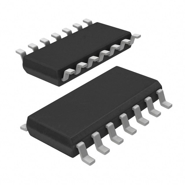
| 描述 | IC OSC PROG TIMER 36MHZ 14SOIC计时器和支持产品 PROGRAMMABLE TIMER |
| 产品分类 | |
| 品牌 | NXP Semiconductors |
| 产品手册 | |
| 产品图片 |
|
| rohs | 符合RoHS无铅 / 符合限制有害物质指令(RoHS)规范要求 |
| 产品系列 | 时钟和计时器IC,计时器和支持产品,NXP Semiconductors HEF4541BT,512- |
| 数据手册 | |
| 产品型号 | HEF4541BT,512 |
| PCN组件/产地 | |
| 产品目录页面 | |
| 产品种类 | 计时器和支持产品 |
| 传播延迟—最大值 | 1150 ns, 420 ns, 300 ns |
| 供应商器件封装 | 14-SO |
| 其它名称 | 568-3137-5 |
| 内部定时器数量 | 1 |
| 包装 | 管件 |
| 商标 | NXP Semiconductors |
| 安装类型 | 表面贴装 |
| 安装风格 | SMD/SMT |
| 封装 | Tube |
| 封装/外壳 | 14-SOIC(0.154",3.90mm 宽) |
| 封装/箱体 | SOT-108 |
| 工作温度 | -40°C ~ 85°C |
| 工厂包装数量 | 1140 |
| 最大工作温度 | + 85 C |
| 最小工作温度 | - 40 C |
| 标准包装 | 57 |
| 电压-电源 | 4.5 V ~ 15.5 V |
| 电流-电源 | 500µA |
| 电源电压-最大 | 15 V |
| 电源电压-最小 | 3 V |
| 类型 | Programmable |
| 计数 | - |
| 零件号别名 | HEF4541BT |
| 频率 | 36MHz |


PDF Datasheet 数据手册内容提取
HEF4541B Programmable timer Rev. 5 — 15 December 2015 Product data sheet 1. General description The HEF4541B is a programmable timer which consists of a 16-stage binary counter, an integrated oscillator to be used with external timing components, an automatic power-on reset and output control logic. The frequency of the oscillator is determined by the external components R and C within the frequency range 1Hz to 100kHz. This oscillator may TC TC be replaced by an external clock signal at input RS, the timer advances on the positive-going transition of RS. A LOW on the auto reset input (AR) and a LOW on the master reset input (MR) enables the internal power-on reset. A HIGH level at input MR resets the counter independent on all other inputs. Resetting disables the oscillator to provide no active power dissipation. A HIGH at input AR turns off the power-on reset to provide a low quiescent power dissipation of the timer. The 16-stage counter divides the oscillator frequency by 28, 210, 213 or 216 depending on the state of the address inputs (A0, A1). The divided oscillator frequency is available at output O. The phase input (PH) features a complementary output signal. When the mode select input (MODE) is LOW the timer is a single transition timer and when HIGH the timer is a 2n frequency divider. It operates over a recommended V power supply range of 3V to 15 V referenced to V DD SS (usually ground). Unused inputs must be connected to V , V , or another input. DD SS 2. Features and benefits Fully static operation 5 V, 10 V, and 15 V parametric ratings Standardized symmetrical output characteristics Operates across the automotive temperature range 40 C to +85 C Complies with JEDEC standard JESD 13-B 3. Ordering information Table 1. Ordering info rmation All types operate from 40C to +85C. Type number Package Name Description Version HEF4541BT SO14 plastic small outline package; 14 leads; body width 3.9 mm SOT108-1
HEF4541B Nexperia Programmable timer 4. Functional diagram (cid:53)(cid:54) (cid:38)(cid:55)(cid:38) (cid:53)(cid:55)(cid:38) (cid:36)(cid:19) (cid:36)(cid:20) (cid:48)(cid:50)(cid:39)(cid:40) (cid:22) (cid:21) (cid:20) (cid:20)(cid:21) (cid:20)(cid:22) (cid:20)(cid:19) (cid:38)(cid:50)(cid:49)(cid:55)(cid:53)(cid:50)(cid:47)(cid:3)(cid:44)(cid:49)(cid:51)(cid:56)(cid:55)(cid:54) (cid:38)(cid:51) (cid:50)(cid:56)(cid:55)(cid:51)(cid:56)(cid:55) (cid:27) (cid:24) (cid:37)(cid:44)(cid:49)(cid:36)(cid:53)(cid:60) (cid:50) (cid:36)(cid:53) (cid:54)(cid:55)(cid:36)(cid:42)(cid:40) (cid:51)(cid:50)(cid:58)(cid:40)(cid:53)(cid:16)(cid:50)(cid:49) (cid:38)(cid:50)(cid:56)(cid:49)(cid:55)(cid:40)(cid:53) (cid:25) (cid:53)(cid:40)(cid:54)(cid:40)(cid:55) (cid:38)(cid:39) (cid:48)(cid:53) (cid:28) (cid:51)(cid:43) (cid:19)(cid:19)(cid:20)(cid:68)(cid:68)(cid:76)(cid:24)(cid:27)(cid:20) Fig 1. Functional diagram (cid:38)(cid:55)(cid:38) (cid:53)(cid:55)(cid:38) (cid:53)(cid:54) (cid:21)(cid:27)(cid:3)(cid:38)(cid:50)(cid:56)(cid:49)(cid:55)(cid:40)(cid:53) (cid:38)(cid:51) (cid:21)(cid:27) (cid:53)(cid:40)(cid:54)(cid:40)(cid:55) (cid:21)(cid:27)(cid:3)(cid:38)(cid:50)(cid:56)(cid:49)(cid:55)(cid:40)(cid:53) (cid:38)(cid:51) (cid:53)(cid:40)(cid:54)(cid:40)(cid:55) (cid:21)(cid:21) (cid:21)(cid:24) (cid:21)(cid:27) (cid:36)(cid:19) (cid:48)(cid:56)(cid:59) (cid:36)(cid:20) (cid:51)(cid:50)(cid:58)(cid:40)(cid:53)(cid:16)(cid:50)(cid:49) (cid:36)(cid:53) (cid:53)(cid:40)(cid:54)(cid:40)(cid:55) (cid:47)(cid:36)(cid:55)(cid:38)(cid:43) (cid:48)(cid:53) (cid:48)(cid:50)(cid:39)(cid:40) (cid:51)(cid:43) (cid:50) (cid:19)(cid:19)(cid:20)(cid:68)(cid:68)(cid:76)(cid:24)(cid:27)(cid:22) Fig 2. Logic diagram HEF4541B All information provided in this document is subject to legal disclaimers. © Nexperia B.V. 2017. All rights reserved Product data sheet Rev. 5 — 15 December 2015 2 of 16
HEF4541B Nexperia Programmable timer 5. Pinning information 5.1 Pinning (cid:43)(cid:40)(cid:41)(cid:23)(cid:24)(cid:23)(cid:20)(cid:37) (cid:53)(cid:55)(cid:38) (cid:20) (cid:20)(cid:23) (cid:57)(cid:39)(cid:39) (cid:38)(cid:55)(cid:38) (cid:21) (cid:20)(cid:22) (cid:36)(cid:20) (cid:53)(cid:54) (cid:22) (cid:20)(cid:21) (cid:36)(cid:19) (cid:81)(cid:17)(cid:70)(cid:17) (cid:23) (cid:20)(cid:20) (cid:81)(cid:17)(cid:70)(cid:17) (cid:36)(cid:53) (cid:24) (cid:20)(cid:19) (cid:48)(cid:50)(cid:39)(cid:40) (cid:48)(cid:53) (cid:25) (cid:28) (cid:51)(cid:43) (cid:57)(cid:54)(cid:54) (cid:26) (cid:27) (cid:50) (cid:19)(cid:19)(cid:20)(cid:68)(cid:68)(cid:76)(cid:24)(cid:27)(cid:21) Fig 3. Pin configuration 5.2 Pin description Table 2. Pin descripti on Symbol Pin Description RTC 1 external resistor connection CTC 2 external capacitor connection RS 3 external resistor connection (RS) or external clock input nc 4, 11 not connected AR 5 auto reset input (active low) MR 6 master reset input V 7 ground (0 V) SS O 8 timer output PH 9 phase input MODE 10 mode select input A0, A1 12, 13 address inputs V 14 supply voltage DD HEF4541B All information provided in this document is subject to legal disclaimers. © Nexperia B.V. 2017. All rights reserved Product data sheet Rev. 5 — 15 December 2015 3 of 16
HEF4541B Nexperia Programmable timer 6. Functional description Table 3. Function tab le[1] Input MODE AR MR PH MODE H L X X auto reset disabled L L X X auto reset enabled[2] X H X X master reset active X L X H normal operation selected division to output X L X L single-cycle mode[3] X L L X output initially LOW after reset X L H X output initially HIGH, after reset [1] H=HIGH voltage level; L=LOW voltage level; X = don’t care. [2] For correct power-on reset, the supply voltage should be above 8.5 V. For V < 8.5 V, disable the autoreset and connect AR to V . DD DD [3] The timer is initialized on a reset pulse and the output changes state after 2n-1 counts and remains in that state (latched). Reset of this latch is obtained by master reset or by a LOW to HIGH transition on the MODE input. Table 4. Frequency s election table A0 A1 Number of counter stages n f n --O----S--C-- = 2 f O L L 13 8192 L H 10 1024 H L 8 256 H H 16 65536 7. Limiting values Table 5. Limiting valu es In accordance with the Absolute Maximum Rating System (IEC 60134). Symbol Parameter Conditions Min Max Unit V supply voltage 0.5 +18 V DD I input clamping current V <0.5V or V >V + 0.5 V - 10 mA IK I I DD V input voltage 0.5 V + 0.5 V I DD I output clamping current V <0.5VorV >V + 0.5 V - 10 mA OK O O DD I input/output current O output - 10 mA I/O T storage temperature 65 +150 C stg T ambient temperature 40 +85 C amb P total power dissipation T = 40C to +85 C tot amb SO14 package [1] - 500 mW P power dissipation - 100 mW [1] For SO14 package: Ptot derates linearly with 8 mW/K above 70 C. HEF4541B All information provided in this document is subject to legal disclaimers. © Nexperia B.V. 2017. All rights reserved Product data sheet Rev. 5 — 15 December 2015 4 of 16
HEF4541B Nexperia Programmable timer 8. Recommended operating conditions Table 6. Recommend ed operating conditions Symbol Parameter Conditions Min Max Unit V supply voltage 3 15 V DD V input voltage 0 V V I DD T ambient temperature in free air 40 +85 C amb t/V input transition rise and fall rate V = 5 V - 3.75 s/V DD V = 10 V - 0.5 s/V DD V = 15 V - 0.08 s/V DD 9. Static characteristics Table 7. Static charac teristics V = 0 V; V = V or V ; unless otherwise specified. SS I SS DD Symbol Parameter Conditions V T = 40 C T = 25 C T = 85 C Unit DD amb amb amb Min Max Min Max Min Max V HIGH-level I <1 A 5 V 3.5 - 3.5 - 3.5 - V IH O inputvoltage 10 V 7.0 - 7.0 - 7.0 - V 15 V 11.0 - 11.0 - 11.0 - V V LOW-level I <1 A 5 V - 1.5 - 1.5 - 1.5 V IL O inputvoltage 10 V - 3.0 - 3.0 - 3.0 V 15 V - 4.0 - 4.0 - 4.0 V V HIGH-level I <1 A 5 V 4.95 - 4.95 - 4.95 - V OH O outputvoltage 10 V 9.95 - 9.95 - 9.95 - V 15 V 14.95 - 14.95 - 14.95 - V V LOW-level I <1 A 5 V - 0.05 - 0.05 - 0.05 V OL O outputvoltage 10 V - 0.05 - 0.05 - 0.05 V 15 V - 0.05 - 0.05 - 0.05 V I HIGH-level CTC, RTC; OH outputcurrent V = 2.5 V 5 V - 1.4 - 1.2 - 0.95 mA O V =4.6V 5 V - 0.5 - 0.4 - 0.3 mA O V = 9.5 V 10 V - 1.4 - 1.2 - 0.95 mA O V = 13.5 V 15 V - 4.8 - 4.0 - 3.2 mA O O; V = 2.5 V 5 V - 1.7 - 1.4 - 1.1 mA O V =4.6V 5 V - 0.64 - 0.5 - 0.36 mA O V = 9.5 V 10 V - 1.6 - 1.3 - 0.9 mA O V = 13.5 V 15 V - 4.2 - 3.4 - 2.4 mA O HEF4541B All information provided in this document is subject to legal disclaimers. © Nexperia B.V. 2017. All rights reserved Product data sheet Rev. 5 — 15 December 2015 5 of 16
HEF4541B Nexperia Programmable timer Table 7. Static characteristics …continued V = 0 V; V = V or V ; unless otherwise specified. SS I SS DD Symbol Parameter Conditions V T = 40 C T = 25 C T = 85 C Unit DD amb amb amb Min Max Min Max Min Max I LOW-level CTC, RTC; OL outputcurrent V = 0.4 V 5 V 0.33 - 0.27 - 0.20 - mA O V = 0.5 V 10 V 1.0 - 0.85 - 0.68 - mA O V = 1.5 V 15 V 3.2 - 2.7 - 2.3 - mA O O; V = 0.4 V 5 V 0.64 - 0.5 - 0.36 - mA O V = 0.5 V 10 V 1.6 - 1.3 - 0.9 - mA O V = 1.5 V 15 V 4.2 - 3.2 - 2.4 - mA O I input leakage 15 V - 0.1 - 0.1 - 1.0 A I current I supply current I = 0A 5 V - 5 - 5 - 150 A DD O 10 V - 10 - 10 - 300 A 15 V - 20 - 20 - 600 A C input capacitance - - - - 7.5 - - pF I Table 8. Reset charac teristics V = 0 V; V = V or V ; see Table12 for test conditions; unless otherwise specified. SS I SS DD Symbol Parameter Conditions V T = 40C T = +25 C T = +85C Unit DD amb amb amb Min Max Min Typ Max Min Max I supply current supply current for 5 V - 80 - 20 80 - 230 A DD power-on reset 10 V - 750 - 250 600 - 700 A enable; AR=MR=0V; Other 15 V - 1.6 - 0.5 1.3 - 1.5 mA inputs at 0V or V DD V supply voltage supply voltage for - - - 8.5 5 - - - V DD automatic reset initialization; AR=MR=0V; Other inputs at 0V or V DD HEF4541B All information provided in this document is subject to legal disclaimers. © Nexperia B.V. 2017. All rights reserved Product data sheet Rev. 5 — 15 December 2015 6 of 16
HEF4541B Nexperia Programmable timer 10. Dynamic characteristics Table 9. Dynamic cha racteristics V = 0 V; T = 25 C unless otherwise specified. For test circuit, see Figure5. SS amb Symbol Parameter Conditions V Extrapolation formula Min Typ[1] Max Unit DD t propagation delay RS to O; 5 V [2] 348 ns + (0.55 ns/pF)C - 375 750 ns pd L 28selected; 10 V 139 ns + (0.23 ns/pF)C - 150 300 ns L seeFigure4 15 V 102 ns + (0.16 ns/pF)C - 110 220 ns L RS to O; 5 V 398 ns + (0.55 ns/pF)C - 425 850 ns L 210selected; 10 V 154 ns + (0.23 ns/pF)C - 165 330 ns L seeFigure4 15 V 112 ns + (0.16 ns/pF)C - 120 240 ns L RS to O; 5 V 483 ns + (0.55 ns/pF)C - 510 1020 ns L 213selected; 10 V 179 ns + (0.23 ns/pF)C - 190 380 ns L seeFigure4 15 V 127 ns + (0.16 ns/pF)C - 135 270 ns L RS to O; 5 V 548 ns + (0.55 ns/pF)C - 575 1150 ns L 216selected; 10 V 199 ns + (0.23 ns/pF)C - 210 420 ns L seeFigure4 15 V 142 ns + (0.16 ns/pF)C - 150 300 ns L t pulse width RS LOW; 5 V [3] 60 30 - ns W MRHIGH; 10 V 30 15 - ns seeFigure4 15 V 24 12 - ns f maximum clock RS; see Figure4 5 V 8 16 - MHz clk(max) frequency 10 V 15 30 - MHz 15 V 18 36 - MHz f oscillator frequency R = 5k; 5 V - 90 - kHz osc t C =1nF; t 10 V - 90 - kHz R =10k; S seeFigure6 15 V - 90 - kHz R = 56 k; 5 V - 8 - kHz t C =1nF; t 10 V - 8 - kHz R =120k; S seeFigure6 15 V - 8 - kHz [1] The typical values of the propagation delay and transition times are calculated from the extrapolation formulas shown (C in pF). L [2] t is the same as t and t . pd PHL PLH [3] t is the same as t and t . W WL(min) WH(min) HEF4541B All information provided in this document is subject to legal disclaimers. © Nexperia B.V. 2017. All rights reserved Product data sheet Rev. 5 — 15 December 2015 7 of 16
HEF4541B Nexperia Programmable timer Table 10. Dynamic po wer dissipation P can be calculated from the formulas shown. V = 0V; t = t 20ns; T = 25 C. D SS r f amb Symbol Parameter V Typical formula DD Per package P dynamic power dissipation 5V P = 1300 f + (f C V 2) W D D i o L DD 10V P = 5300 f + (f C V 2)W D i o L DD 15V P = 12000 f + (f C V 2) W D i o L DD Using the on-chip oscillator P Total dynamic power dissipation 5V P = 1300 f + f C V 2 + 2C V 2 f + 10V W D(Tot) D osc o L DD TC DD osc DD 10V P = 5300 f + f C V 2 + 2C V 2 f + 100V W D osc o L DD TC DD osc DD 15V P = 12000 f + f C V 2 + 2C V 2 f + 400V W D osc o L DD TC DD osc DD [1] f =inputfrequencyinMHz; f = output frequency in MHz; C = output load capacitance in pF; V =supplyvoltageinV; i o L DD fosc=oscillatorfrequency in MHz; CTC=timingcapacitanceinpF. 11. Waveforms (cid:11)(cid:20)(cid:12) (cid:20)(cid:18)(cid:73)(cid:70)(cid:79)(cid:78)(cid:11)(cid:80)(cid:68)(cid:91)(cid:12) (cid:57)(cid:44) (cid:53)(cid:54)(cid:3)(cid:76)(cid:81)(cid:83)(cid:88)(cid:87) (cid:57)(cid:48) (cid:57)(cid:54)(cid:54) (cid:87)(cid:58)(cid:43)(cid:11)(cid:80)(cid:76)(cid:81)(cid:12) (cid:87)(cid:51)(cid:47)(cid:43) (cid:87)(cid:58)(cid:47)(cid:11)(cid:80)(cid:76)(cid:81)(cid:12) (cid:87)(cid:51)(cid:43)(cid:47) (cid:57)(cid:50)(cid:43) (cid:50)(cid:3)(cid:82)(cid:88)(cid:87)(cid:83)(cid:88)(cid:87) (cid:57)(cid:48) (cid:57)(cid:50)(cid:47) (cid:57)(cid:44) (cid:48)(cid:53)(cid:3)(cid:76)(cid:81)(cid:83)(cid:88)(cid:87) (cid:57)(cid:54)(cid:54) (cid:87)(cid:58)(cid:43)(cid:11)(cid:80)(cid:76)(cid:81)(cid:12) (cid:68)(cid:68)(cid:68)(cid:16)(cid:19)(cid:19)(cid:22)(cid:22)(cid:28)(cid:20) V and V are typical output voltage levels that occur with the output load. OL OH Measurement are points given in Table11, the test circuit in Figure5 and the test data in Table12 (1) 2n pulses as selected by address inputs (A0, A1). Fig 4. Propagation delay clock (RS) to output (O), clock pulse width and maximum clock frequency Table 11. Measuremen t points Supply voltage Input Output V V V DD M M 5V to 15V 0.5V 0.5V DD DD HEF4541B All information provided in this document is subject to legal disclaimers. © Nexperia B.V. 2017. All rights reserved Product data sheet Rev. 5 — 15 December 2015 8 of 16
HEF4541B Nexperia Programmable timer (cid:57)(cid:39)(cid:39) (cid:57)(cid:44) (cid:57)(cid:50) (cid:42) (cid:39)(cid:56)(cid:55) (cid:53)(cid:55) (cid:38)(cid:47) (cid:19)(cid:19)(cid:20)(cid:68)(cid:68)(cid:74)(cid:20)(cid:27)(cid:21) Test data is given in Table12. Definitions for test circuit: DUT - Device Under Test. RL = Load resistance. CL = load capacitance. R = Termination resistance should be equal to output impedance of Z of the pulse generator. T o Fig 5. Test circuit for measuring switching times Table 12. Test data Supply Input Load V V t, t C DD I r f L 5V to 15V V or V 20 ns 50 pF SS DD HEF4541B All information provided in this document is subject to legal disclaimers. © Nexperia B.V. 2017. All rights reserved Product data sheet Rev. 5 — 15 December 2015 9 of 16
HEF4541B Nexperia Programmable timer 12. Application information RC oscillator timing component limitations The oscillator frequency is mainly determined by R C , provided R << R and TC TC TC S R C <<R C . The function of R is to minimize the influence of the forward voltage S 2 TC TC S across the input protection diodes on the frequency. The stray capacitance C should be 2 kept as small as possible. In consideration of accuracy, C must be larger than the TC inherent stray capacitance. R must be larger than the LOCMOS ‘ON’ resistance in TC series with it, which typically is 500 at V = 5 V, 300 at V = 10 V and 200 at DD DD V =15V. DD The recommended values for these components to maintain agreement with the typical oscillation formula are: C 100 pF, up to any typical value, 10 k R 1 M. TC TC (cid:85)(cid:72)(cid:86)(cid:72)(cid:87) (cid:70)(cid:79)(cid:82)(cid:70)(cid:78)(cid:3)(cid:87)(cid:82)(cid:3) (cid:73)(cid:85)(cid:82)(cid:80)(cid:3)(cid:79)(cid:82)(cid:74)(cid:76)(cid:70) (cid:70)(cid:82)(cid:88)(cid:81)(cid:87)(cid:72)(cid:85) (cid:53)(cid:54) (cid:38)(cid:55)(cid:38) (cid:53)(cid:55)(cid:38) (cid:22) (cid:21) (cid:20) (cid:38)(cid:21) (cid:53)(cid:54) (cid:38)(cid:55)(cid:38) (cid:53)(cid:55)(cid:38) (cid:19)(cid:19)(cid:20)(cid:68)(cid:68)(cid:76)(cid:24)(cid:27)(cid:23) 1 Typical formula for oscillator frequency: f = ----------------------------------------. osc 2.3R C TC TC Fig 6. External component connection for RC oscillator; R ≈ R S TC (cid:20)(cid:19)(cid:24) (cid:19)(cid:19)(cid:20)(cid:68)(cid:68)(cid:76)(cid:24)(cid:27)(cid:25) (cid:20)(cid:19)(cid:24) (cid:19)(cid:19)(cid:20)(cid:68)(cid:68)(cid:76)(cid:24)(cid:27)(cid:24) (cid:73)(cid:82)(cid:86)(cid:70) (cid:73)(cid:82)(cid:86)(cid:70) (cid:11)(cid:43)(cid:93)(cid:12) (cid:11)(cid:43)(cid:93)(cid:12) (cid:20)(cid:19)(cid:23) (cid:20)(cid:19)(cid:23) (cid:20)(cid:19)(cid:22) (cid:20)(cid:19)(cid:22) (cid:20)(cid:19)(cid:21) (cid:20)(cid:19)(cid:21) (cid:20)(cid:19) (cid:20)(cid:19) (cid:20)(cid:19)(cid:16)(cid:23) (cid:20)(cid:19)(cid:16)(cid:22) (cid:20)(cid:19)(cid:16)(cid:21) (cid:20)(cid:19)(cid:16)(cid:20) (cid:20)(cid:19)(cid:22) (cid:20)(cid:19)(cid:23) (cid:20)(cid:19)(cid:24) (cid:20)(cid:19)(cid:25) (cid:38)(cid:55)(cid:38)(cid:3)(cid:11) (cid:41)(cid:12) (cid:53)(cid:55)(cid:38)(cid:3)(cid:11) (cid:12) a. C curve at R = 56 k; RS = 120 k. b. R curve at C = 1 nF; RS = 2 R . TC TC TC TC TC Fig 7. RC oscillator frequency as a function of R and C at V = 5 to 15 V; T = 25 C TC TC DD amb HEF4541B All information provided in this document is subject to legal disclaimers. © Nexperia B.V. 2017. All rights reserved Product data sheet Rev. 5 — 15 December 2015 10 of 16
HEF4541B Nexperia Programmable timer (cid:19)(cid:19)(cid:20)(cid:68)(cid:68)(cid:76)(cid:24)(cid:27)(cid:26) (cid:19)(cid:19)(cid:20)(cid:68)(cid:68)(cid:76)(cid:24)(cid:27)(cid:27) (cid:20)(cid:19) (cid:20)(cid:19) (cid:73) (cid:73) (cid:11)(cid:8)(cid:12) (cid:11)(cid:8)(cid:12) (cid:24) (cid:24) (cid:57)(cid:39)(cid:39)(cid:3)(cid:32)(cid:3)(cid:20)(cid:24)(cid:3)(cid:57) (cid:20)(cid:19)(cid:3)(cid:57) (cid:57)(cid:39)(cid:39)(cid:3)(cid:32)(cid:3)(cid:20)(cid:24)(cid:3)(cid:57) (cid:19) (cid:19) (cid:20)(cid:19)(cid:3)(cid:57) (cid:24)(cid:3)(cid:57) (cid:16)(cid:24) (cid:16)(cid:24) (cid:24)(cid:3)(cid:57) (cid:16)(cid:20)(cid:19) (cid:16)(cid:20)(cid:19) (cid:16)(cid:26)(cid:24) (cid:16)(cid:21)(cid:24) (cid:21)(cid:24) (cid:26)(cid:24) (cid:20)(cid:21)(cid:24) (cid:16)(cid:26)(cid:24) (cid:16)(cid:21)(cid:24) (cid:21)(cid:24) (cid:26)(cid:24) (cid:20)(cid:21)(cid:24) (cid:55)(cid:68)(cid:80)(cid:69)(cid:3)(cid:11)(cid:131)(cid:38)(cid:12) (cid:55)(cid:68)(cid:80)(cid:69)(cid:3)(cid:11)(cid:131)(cid:38)(cid:12) a. R = 56 k; C = 1 nF; RS = 0 . b. R = 56 k; C = 1 nF; RS = 120 k. TC TC TC TC Fig 8. Frequency deviation (f) as a function of ambient temperature HEF4541B All information provided in this document is subject to legal disclaimers. © Nexperia B.V. 2017. All rights reserved Product data sheet Rev. 5 — 15 December 2015 11 of 16
HEF4541B Nexperia Programmable timer 13. Package outline (cid:54)(cid:50)(cid:20)(cid:23)(cid:29)(cid:3)(cid:83)(cid:79)(cid:68)(cid:86)(cid:87)(cid:76)(cid:70)(cid:3)(cid:86)(cid:80)(cid:68)(cid:79)(cid:79)(cid:3)(cid:82)(cid:88)(cid:87)(cid:79)(cid:76)(cid:81)(cid:72)(cid:3)(cid:83)(cid:68)(cid:70)(cid:78)(cid:68)(cid:74)(cid:72)(cid:30)(cid:3)(cid:20)(cid:23)(cid:3)(cid:79)(cid:72)(cid:68)(cid:71)(cid:86)(cid:30)(cid:3)(cid:69)(cid:82)(cid:71)(cid:92)(cid:3)(cid:90)(cid:76)(cid:71)(cid:87)(cid:75)(cid:3)(cid:22)(cid:17)(cid:28)(cid:3)(cid:80)(cid:80)(cid:3) (cid:54)(cid:50)(cid:55)(cid:20)(cid:19)(cid:27)(cid:16)(cid:20)(cid:3) (cid:39)(cid:3) (cid:40)(cid:3) (cid:36)(cid:3) (cid:59)(cid:3) (cid:70)(cid:3) (cid:92)(cid:3) (cid:43)(cid:3)(cid:40)(cid:3) (cid:89)(cid:3)(cid:48)(cid:3) (cid:36)(cid:3) (cid:61)(cid:3) (cid:20)(cid:23)(cid:3) (cid:27)(cid:3) (cid:52)(cid:3) (cid:36)(cid:3)(cid:21)(cid:3)(cid:36)(cid:3)(cid:20)(cid:3) (cid:11)(cid:36)(cid:3)(cid:22)(cid:3)(cid:3)(cid:12)(cid:3) (cid:36)(cid:3) (cid:83)(cid:76)(cid:81)(cid:3)(cid:20)(cid:3)(cid:76)(cid:81)(cid:71)(cid:72)(cid:91)(cid:3) (cid:537)(cid:3) (cid:47)(cid:3)(cid:83)(cid:3) (cid:20)(cid:3) (cid:26)(cid:3) (cid:47)(cid:3) (cid:72)(cid:3) (cid:90)(cid:3)(cid:48)(cid:3) (cid:71)(cid:72)(cid:87)(cid:68)(cid:76)(cid:79)(cid:3)(cid:59)(cid:3) (cid:69)(cid:3)(cid:83)(cid:3) (cid:19)(cid:3) (cid:21)(cid:17)(cid:24)(cid:3) (cid:24)(cid:3)(cid:80)(cid:80)(cid:3) (cid:86)(cid:70)(cid:68)(cid:79)(cid:72)(cid:3) (cid:39)(cid:44)(cid:48)(cid:40)(cid:49)(cid:54)(cid:44)(cid:50)(cid:49)(cid:54)(cid:3)(cid:11)(cid:76)(cid:81)(cid:70)(cid:75)(cid:3)(cid:71)(cid:76)(cid:80)(cid:72)(cid:81)(cid:86)(cid:76)(cid:82)(cid:81)(cid:86)(cid:3)(cid:68)(cid:85)(cid:72)(cid:3)(cid:71)(cid:72)(cid:85)(cid:76)(cid:89)(cid:72)(cid:71)(cid:3)(cid:73)(cid:85)(cid:82)(cid:80)(cid:3)(cid:87)(cid:75)(cid:72)(cid:3)(cid:82)(cid:85)(cid:76)(cid:74)(cid:76)(cid:81)(cid:68)(cid:79)(cid:3)(cid:80)(cid:80)(cid:3)(cid:71)(cid:76)(cid:80)(cid:72)(cid:81)(cid:86)(cid:76)(cid:82)(cid:81)(cid:86)(cid:12)(cid:3) (cid:56)(cid:49)(cid:44)(cid:55)(cid:3) (cid:80)(cid:36)(cid:68)(cid:91)(cid:3)(cid:17)(cid:3) (cid:36)(cid:3)(cid:20)(cid:3) (cid:36)(cid:3)(cid:21)(cid:3) (cid:36)(cid:3)(cid:22)(cid:3) (cid:69)(cid:3)(cid:83)(cid:3) (cid:70)(cid:3) (cid:39)(cid:3)(cid:11)(cid:20)(cid:12)(cid:3) (cid:40)(cid:3)(cid:11)(cid:20)(cid:12)(cid:3) (cid:72)(cid:3) (cid:43)(cid:3)(cid:40)(cid:3) (cid:47)(cid:3) (cid:47)(cid:3)(cid:83)(cid:3) (cid:52)(cid:3) (cid:89)(cid:3) (cid:90)(cid:3) (cid:92)(cid:3) (cid:61)(cid:3)(cid:11)(cid:20)(cid:12)(cid:3) (cid:537)(cid:3) (cid:80)(cid:80)(cid:3) (cid:20)(cid:17)(cid:26)(cid:24)(cid:3) (cid:19)(cid:17)(cid:21)(cid:24)(cid:3) (cid:20)(cid:17)(cid:23)(cid:24)(cid:3) (cid:19)(cid:17)(cid:21)(cid:24)(cid:3) (cid:19)(cid:17)(cid:23)(cid:28)(cid:3) (cid:19)(cid:17)(cid:21)(cid:24)(cid:3) (cid:27)(cid:17)(cid:26)(cid:24)(cid:3) (cid:23)(cid:17)(cid:19)(cid:3) (cid:20)(cid:17)(cid:21)(cid:26)(cid:3) (cid:25)(cid:17)(cid:21)(cid:3) (cid:20)(cid:17)(cid:19)(cid:3)(cid:24)(cid:3) (cid:20)(cid:17)(cid:19)(cid:3) (cid:19)(cid:17)(cid:26)(cid:3) (cid:19)(cid:17)(cid:21)(cid:24)(cid:3) (cid:19)(cid:17)(cid:21)(cid:24)(cid:3) (cid:19)(cid:17)(cid:20)(cid:3) (cid:19)(cid:17)(cid:26)(cid:3) (cid:19)(cid:17)(cid:20)(cid:19)(cid:3) (cid:20)(cid:17)(cid:21)(cid:24)(cid:3) (cid:19)(cid:17)(cid:22)(cid:25)(cid:3) (cid:19)(cid:17)(cid:20)(cid:28)(cid:3) (cid:27)(cid:17)(cid:24)(cid:24)(cid:3) (cid:22)(cid:17)(cid:27)(cid:3) (cid:24)(cid:17)(cid:27)(cid:3) (cid:19)(cid:17)(cid:23)(cid:3) (cid:19)(cid:17)(cid:25)(cid:3) (cid:19)(cid:17)(cid:22)(cid:3) (cid:27)(cid:3)(cid:82)(cid:3) (cid:19)(cid:17)(cid:19)(cid:20)(cid:19)(cid:3) (cid:19)(cid:17)(cid:19)(cid:24)(cid:26)(cid:3) (cid:19)(cid:17)(cid:19)(cid:20)(cid:28)(cid:3)(cid:19)(cid:17)(cid:19)(cid:20)(cid:19)(cid:19)(cid:3) (cid:19)(cid:17)(cid:22)(cid:24)(cid:3) (cid:19)(cid:17)(cid:20)(cid:25)(cid:3) (cid:19)(cid:17)(cid:21)(cid:23)(cid:23)(cid:3) (cid:19)(cid:17)(cid:19)(cid:22)(cid:28)(cid:3) (cid:19)(cid:17)(cid:19)(cid:21)(cid:27)(cid:3) (cid:19)(cid:17)(cid:19)(cid:21)(cid:27)(cid:3) (cid:19)(cid:3)(cid:82)(cid:3) (cid:76)(cid:81)(cid:70)(cid:75)(cid:72)(cid:86)(cid:3) (cid:19)(cid:17)(cid:19)(cid:25)(cid:28)(cid:3) (cid:19)(cid:17)(cid:19)(cid:20)(cid:3) (cid:19)(cid:17)(cid:19)(cid:24)(cid:3) (cid:19)(cid:17)(cid:19)(cid:23)(cid:20)(cid:3) (cid:19)(cid:17)(cid:19)(cid:20)(cid:3) (cid:19)(cid:17)(cid:19)(cid:20)(cid:3) (cid:19)(cid:17)(cid:19)(cid:19)(cid:23)(cid:3) (cid:19)(cid:17)(cid:19)(cid:19)(cid:23)(cid:3) (cid:19)(cid:17)(cid:19)(cid:23)(cid:28)(cid:3) (cid:19)(cid:17)(cid:19)(cid:20)(cid:23)(cid:3)(cid:19)(cid:17)(cid:19)(cid:19)(cid:26)(cid:24)(cid:3) (cid:19)(cid:17)(cid:22)(cid:23)(cid:3) (cid:19)(cid:17)(cid:20)(cid:24)(cid:3) (cid:19)(cid:17)(cid:21)(cid:21)(cid:27)(cid:3) (cid:19)(cid:17)(cid:19)(cid:20)(cid:25)(cid:3) (cid:19)(cid:17)(cid:19)(cid:21)(cid:23)(cid:3) (cid:19)(cid:17)(cid:19)(cid:20)(cid:21)(cid:3) (cid:49)(cid:82)(cid:87)(cid:72)(cid:3) (cid:20)(cid:17)(cid:3)(cid:51)(cid:79)(cid:68)(cid:86)(cid:87)(cid:76)(cid:70)(cid:3)(cid:82)(cid:85)(cid:3)(cid:80)(cid:72)(cid:87)(cid:68)(cid:79)(cid:3)(cid:83)(cid:85)(cid:82)(cid:87)(cid:85)(cid:88)(cid:86)(cid:76)(cid:82)(cid:81)(cid:86)(cid:3)(cid:82)(cid:73)(cid:3)(cid:19)(cid:17)(cid:20)(cid:24)(cid:3)(cid:80)(cid:80)(cid:3)(cid:11)(cid:19)(cid:17)(cid:19)(cid:19)(cid:25)(cid:3)(cid:76)(cid:81)(cid:70)(cid:75)(cid:12)(cid:3)(cid:80)(cid:68)(cid:91)(cid:76)(cid:80)(cid:88)(cid:80)(cid:3)(cid:83)(cid:72)(cid:85)(cid:3)(cid:86)(cid:76)(cid:71)(cid:72)(cid:3)(cid:68)(cid:85)(cid:72)(cid:3)(cid:81)(cid:82)(cid:87)(cid:3)(cid:76)(cid:81)(cid:70)(cid:79)(cid:88)(cid:71)(cid:72)(cid:71)(cid:17)(cid:3)(cid:3) (cid:50)(cid:56)(cid:55)(cid:47)(cid:44)(cid:49)(cid:40)(cid:3) (cid:3)(cid:53)(cid:40)(cid:41)(cid:40)(cid:53)(cid:40)(cid:49)(cid:38)(cid:40)(cid:54)(cid:3) (cid:40)(cid:56)(cid:53)(cid:50)(cid:51)(cid:40)(cid:36)(cid:49)(cid:3) (cid:44)(cid:54)(cid:54)(cid:56)(cid:40)(cid:3)(cid:39)(cid:36)(cid:55)(cid:40)(cid:3) (cid:57)(cid:40)(cid:53)(cid:54)(cid:44)(cid:50)(cid:49)(cid:3) (cid:3)(cid:44)(cid:40)(cid:38)(cid:3) (cid:3)(cid:45)(cid:40)(cid:39)(cid:40)(cid:38)(cid:3) (cid:3)(cid:45)(cid:40)(cid:44)(cid:55)(cid:36)(cid:3) (cid:51)(cid:53)(cid:50)(cid:45)(cid:40)(cid:38)(cid:55)(cid:44)(cid:50)(cid:49)(cid:3) (cid:28)(cid:28)(cid:16)(cid:20)(cid:21)(cid:16)(cid:21)(cid:26)(cid:3) (cid:3)(cid:54)(cid:50)(cid:55)(cid:20)(cid:19)(cid:27)(cid:16)(cid:20)(cid:3) (cid:3)(cid:19)(cid:26)(cid:25)(cid:40)(cid:19)(cid:25)(cid:3) (cid:3)(cid:48)(cid:54)(cid:16)(cid:19)(cid:20)(cid:21)(cid:3) (cid:19)(cid:22)(cid:16)(cid:19)(cid:21)(cid:16)(cid:20)(cid:28)(cid:3) Fig 9. Package outline SOT108-1 (SO14) HEF4541B All information provided in this document is subject to legal disclaimers. © Nexperia B.V. 2017. All rights reserved Product data sheet Rev. 5 — 15 December 2015 12 of 16
HEF4541B Nexperia Programmable timer 14. Abbreviations Table 13. Abbreviation s Acronym Description CMOS Complementary Metal Oxide Semiconductor DUT Device Under Test ESD ElectroStatic Discharge HBM Human Body Model MM Machine Model TTL Transistor-Transistor Logic 15. Revision history T able 14. Revision history Document ID Release date Data sheet status Change notice Supersedes HEF4541B v.5 20151215 Product data sheet - HEF4541B v.4 Modifications: • Type number HEF4541BP (SOT27-1) removed. HEF4541B v.4 20120625 Product data sheet - HEF4541B_CNV v.3 Modifications: • The format of this data sheet has been redesigned to comply with the new identity guidelines of NXP Semiconductors. • Legal texts have been adapted to the new company name where appropriate. • Section 2 “Features and benefits” added. HEF4541B_CNV v.3 19950101 Product specification - HEF4541B_CNV v.2 HEF4541B_CNV v.2 19950101 Product specification - - HEF4541B All information provided in this document is subject to legal disclaimers. © Nexperia B.V. 2017. All rights reserved Product data sheet Rev. 5 — 15 December 2015 13 of 16
HEF4541B Nexperia Programmable timer 16. Legal information 16.1 Data sheet status Document status[1][2] Product status[3] Definition Objective [short] data sheet Development This document contains data from the objective specification for product development. Preliminary [short] data sheet Qualification This document contains data from the preliminary specification. Product [short] data sheet Production This document contains the product specification. [1] Please consult the most recently issued document before initiating or completing a design. [2] The term ‘short data sheet’ is explained in section “Definitions”. [3] The product status of device(s) described in this document may have changed since this document was published and may differ in case of multiple devices. The latest product status information is available on the Internet at URL http://www.nexperia.com. 16.2 Definitions Suitability for use — Nexperia products are not designed, authorized or warranted to be suitable for use in life support, life-critical or safety-critical systems or equipment, nor in applications where failure or Draft — The document is a draft version only. The content is still under malfunction of a Nexperia product can reasonably be expected internal review and subject to formal approval, which may result in to result in personal injury, death or severe property or environmental modifications or additions. Nexperia does not give any damage. Nexperia and its suppliers accept no liability for representations or warranties as to the accuracy or completeness of inclusion and/or use of Nexperia products in such equipment or information included herein and shall have no liability for the consequences of applications and therefore such inclusion and/or use is at the customer’s own use of such information. risk. Short data sheet — A short data sheet is an extract from a full data sheet Applications — Applications that are described herein for any of these with the same product type number(s) and title. A short data sheet is intended products are for illustrative purposes only. Nexperia makes no for quick reference only and should not be relied upon to contain detailed and representation or warranty that such applications will be suitable for the full information. For detailed and full information see the relevant full data specified use without further testing or modification. sheet, which is available on request via the local Nexperia sales office. In case of any inconsistency or conflict with the short data sheet, the Customers are responsible for the design and operation of their applications full data sheet shall prevail. and products using Nexperia products, and Nexperia accepts no liability for any assistance with applications or customer product Product specification — The information and data provided in a Product design. It is customer’s sole responsibility to determine whether the Nexperia data sheet shall define the specification of the product as agreed between product is suitable and fit for the customer’s applications and Nexperia and its customer, unless Nexperia and products planned, as well as for the planned application and use of customer have explicitly agreed otherwise in writing. In no event however, customer’s third party customer(s). Customers should provide appropriate shall an agreement be valid in which the Nexperia product is design and operating safeguards to minimize the risks associated with their deemed to offer functions and qualities beyond those described in the applications and products. Product data sheet. Nexperia does not accept any liability related to any default, damage, costs or problem which is based on any weakness or default in the 16.3 Disclaimers customer’s applications or products, or the application or use by customer’s third party customer(s). Customer is responsible for doing all necessary testing for the customer’s applications and products using Nexperia Limited warranty and liability — Information in this document is believed to products in order to avoid a default of the applications and be accurate and reliable. However, Nexperia does not give any the products or of the application or use by customer’s third party representations or warranties, expressed or implied, as to the accuracy or customer(s). Nexperia does not accept any liability in this respect. completeness of such information and shall have no liability for the consequences of use of such information. Nexperia takes no Limiting values — Stress above one or more limiting values (as defined in responsibility for the content in this document if provided by an information the Absolute Maximum Ratings System of IEC60134) will cause permanent source outside of Nexperia. damage to the device. Limiting values are stress ratings only and (proper) operation of the device at these or any other conditions above those given in In no event shall Nexperia be liable for any indirect, incidental, the Recommended operating conditions section (if present) or the punitive, special or consequential damages (including - without limitation - lost Characteristics sections of this document is not warranted. Constant or profits, lost savings, business interruption, costs related to the removal or repeated exposure to limiting values will permanently and irreversibly affect replacement of any products or rework charges) whether or not such the quality and reliability of the device. damages are based on tort (including negligence), warranty, breach of contract or any other legal theory. Terms and conditions of commercial sale — Nexperia products are sold subject to the general terms and conditions of commercial Notwithstanding any damages that customer might incur for any reason whatsoever, Nexperia’s aggregate and cumulative liability towards sale, as published at http://www.nexperia.com/profile/terms, unless otherwise agreed in a valid written individual agreement. In case an individual customer for the products described herein shall be limited in accordance agreement is concluded only the terms and conditions of the respective with the Terms and conditions of commercial sale of Nexperia. agreement shall apply. Nexperia hereby expressly objects to Right to make changes — Nexperia reserves the right to make applying the customer’s general terms and conditions with regard to the changes to information published in this document, including without purchase of Nexperia products by customer. limitation specifications and product descriptions, at any time and without notice. This document supersedes and replaces all information supplied prior No offer to sell or license — Nothing in this document may be interpreted or to the publication hereof. construed as an offer to sell products that is open for acceptance or the grant, conveyance or implication of any license under any copyrights, patents or other industrial or intellectual property rights. HEF4541B All information provided in this document is subject to legal disclaimers. © Nexperia B.V. 2017. All rights reserved Product data sheet Rev. 5 — 15 December 2015 14 of 16
HEF4541B Nexperia Programmable timer Export control — This document as well as the item(s) described herein Nexperia’s specifications such use shall be solely at customer’s may be subject to export control regulations. Export might require a prior own risk, and (c) customer fully indemnifies Nexperia for any authorization from competent authorities. liability, damages or failed product claims resulting from customer design and use of the product for automotive applications beyond Nexperia’s Non-automotive qualified products — Unless this data sheet expressly standard warranty and Nexperia’s product specifications. states that this specific Nexperia product is automotive qualified, the product is not suitable for automotive use. It is neither qualified nor tested Translations — A non-English (translated) version of a document is for in accordance with automotive testing or application requirements. Nexperia reference only. The English version shall prevail in case of any discrepancy accepts no liability for inclusion and/or use of between the translated and English versions. non-automotive qualified products in automotive equipment or applications. In the event that customer uses the product for design-in and use in 16.4 Trademarks automotive applications to automotive specifications and standards, customer (a) shall use the product without Nexperia’s warranty of the Notice: All referenced brands, product names, service names and trademarks product for such automotive applications, use and specifications, and (b) are the property of their respective owners. whenever customer uses the product for automotive applications beyond 17. Contact information For more information, please visit: http://www.nexperia.com For sales office addresses, please send an email to: salesaddresses@nexperia.com HEF4541B All information provided in this document is subject to legal disclaimers. © Nexperia B.V. 2017. All rights reserved Product data sheet Rev. 5 — 15 December 2015 15 of 16
HEF4541B Nexperia Programmable timer 18. Contents 1 General description. . . . . . . . . . . . . . . . . . . . . . 1 2 Features and benefits . . . . . . . . . . . . . . . . . . . . 1 3 Ordering information. . . . . . . . . . . . . . . . . . . . . 1 4 Functional diagram . . . . . . . . . . . . . . . . . . . . . . 2 5 Pinning information. . . . . . . . . . . . . . . . . . . . . . 3 5.1 Pinning . . . . . . . . . . . . . . . . . . . . . . . . . . . . . . . 3 5.2 Pin description . . . . . . . . . . . . . . . . . . . . . . . . . 3 6 Functional description . . . . . . . . . . . . . . . . . . . 4 7 Limiting values. . . . . . . . . . . . . . . . . . . . . . . . . . 4 8 Recommended operating conditions. . . . . . . . 5 9 Static characteristics. . . . . . . . . . . . . . . . . . . . . 5 10 Dynamic characteristics. . . . . . . . . . . . . . . . . . 7 11 Waveforms . . . . . . . . . . . . . . . . . . . . . . . . . . . . . 8 12 Application information. . . . . . . . . . . . . . . . . . 10 RC oscillator timing component limitations. . . .10 13 Package outline. . . . . . . . . . . . . . . . . . . . . . . . 12 14 Abbreviations. . . . . . . . . . . . . . . . . . . . . . . . . . 13 15 Revision history. . . . . . . . . . . . . . . . . . . . . . . . 13 16 Legal information. . . . . . . . . . . . . . . . . . . . . . . 14 16.1 Data sheet status . . . . . . . . . . . . . . . . . . . . . . 14 16.2 Definitions. . . . . . . . . . . . . . . . . . . . . . . . . . . . 14 16.3 Disclaimers. . . . . . . . . . . . . . . . . . . . . . . . . . . 14 16.4 Trademarks. . . . . . . . . . . . . . . . . . . . . . . . . . . 15 17 Contact information. . . . . . . . . . . . . . . . . . . . . 15 18 Contents. . . . . . . . . . . . . . . . . . . . . . . . . . . . . . 16 © Nexperia B.V. 2017. All rights reserved For more information, please visit: http://www.nexperia.com For sales office addresses, please send an email to: salesaddresses@nexperia.com Date of release: 15 December 2015
Mouser Electronics Authorized Distributor Click to View Pricing, Inventory, Delivery & Lifecycle Information: N experia: HEF4541BT,653 HEF4541BT,512 HEF4541BT,518