ICGOO在线商城 > 隔离器 > 光隔离器 - 晶体管,光电输出 > HCPL-4504
 Datasheet下载
- 型号: HCPL-4504
- 制造商: Avago Technologies
- 库位|库存: xxxx|xxxx
- 要求:
| 数量阶梯 | 香港交货 | 国内含税 |
| +xxxx | $xxxx | ¥xxxx |
查看当月历史价格
查看今年历史价格
HCPL-4504产品简介:
ICGOO电子元器件商城为您提供HCPL-4504由Avago Technologies设计生产,在icgoo商城现货销售,并且可以通过原厂、代理商等渠道进行代购。 HCPL-4504价格参考。Avago TechnologiesHCPL-4504封装/规格:光隔离器 - 晶体管,光电输出, 光隔离器 晶体管 输出 3750Vrms 1 通道 8-DIP。您可以下载HCPL-4504参考资料、Datasheet数据手册功能说明书,资料中有HCPL-4504 详细功能的应用电路图电压和使用方法及教程。
| 参数 | 数值 |
| 产品目录 | |
| 描述 | OPTOISOLATOR 3.75KV TRANS 8-DIP |
| 产品分类 | |
| 品牌 | Avago Technologies US Inc. |
| 数据手册 | http://www.avagotech.com/docs/AV02-0867EN |
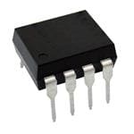
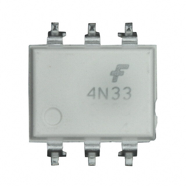
| 产品图片 |
|
| 产品型号 | HCPL-4504 |
| PCN封装 | |
| rohs | 含铅 / 不符合限制有害物质指令(RoHS)规范要求 |
| 产品系列 | - |
| Vce饱和值(最大值) | - |
| 上升/下降时间(典型值) | - |
| 产品目录绘图 |
|
| 供应商器件封装 | 8-DIP |
| 其它名称 | 516-1035-5 |
| 包装 | 管件 |
| 安装类型 | 通孔 |
| 封装/外壳 | 8-DIP(0.300",7.62mm) |
| 工作温度 | -55°C ~ 100°C |
| 打开/关闭时间(典型值) | 200ns, 300ns |
| 标准包装 | 50 |
| 电压-正向(Vf)(典型值) | 1.5V |
| 电压-输出(最大值) | 20V |
| 电压-隔离 | 3750Vrms |
| 电流-DC正向(If) | 25mA |
| 电流-输出/通道 | 8mA |
| 电流传输比(最大值) | 60% @ 16mA |
| 电流传输比(最小值) | 25% @ 16mA |
| 输入类型 | DC |
| 输出类型 | 晶体管 |
| 通道数 | 1 |


.jpg)

- 商务部:美国ITC正式对集成电路等产品启动337调查
- 曝三星4nm工艺存在良率问题 高通将骁龙8 Gen1或转产台积电
- 太阳诱电将投资9.5亿元在常州建新厂生产MLCC 预计2023年完工
- 英特尔发布欧洲新工厂建设计划 深化IDM 2.0 战略
- 台积电先进制程称霸业界 有大客户加持明年业绩稳了
- 达到5530亿美元!SIA预计今年全球半导体销售额将创下新高
- 英特尔拟将自动驾驶子公司Mobileye上市 估值或超500亿美元
- 三星加码芯片和SET,合并消费电子和移动部门,撤换高东真等 CEO
- 三星电子宣布重大人事变动 还合并消费电子和移动部门
- 海关总署:前11个月进口集成电路产品价值2.52万亿元 增长14.8%

.jpg)


.jpg)
PDF Datasheet 数据手册内容提取
HCPL-4504/J454/0454, HCNW4504 High CMR, High Speed Optocouplers Data Sheet Lead (Pb) Free RoHS 6 fully compliant RoHS 6 fully compliant options available; -xxxE denotes a lead-free product Description Features The HCPL-4504 and HCPL-0454 contain a GaAsP LED • Short propagation delays for TTL and IPM applications while the HCPL-J454 and HCNW4504 contain an AlGaAs • 15 kV/µs minimum Common Mode Transient immu- LED. The LED is optically coupled to an integrated high nity at V = 1500 V for TTL/load drive CM gain photo detector. • High CTR at T = 25°C A >25% for HCPL-4504/0454 The HCPL-4504 series has short propagation delays and >23% for HCNW4504 high CTR. The HCPL-4504 series also has a guaranteed >19% for HCPL-J454 propagation delay difference (t -t ). These features PLH PHL make the HCPL-4504 series an excellent solution to IPM • Electrical specifications for common IPM applications inverter dead time and other switching problems. The • TTL compatible CTR, propagation delay, and CMR are specified both for • Open collector output TTL and IPM conditions which are provided for ease of • Safety approval: application. These single channel, diode-transistor opto- UL recognized couplers are available in 8-Pin DIP, SO-8, and Widebody – 3750 V rms/1min. for HCPL-4504/0454/J454 package configurations. An insulating layer between a – 5000 V rms/1min. for HCPL-4504 Option 020 and LED and an integrated photodetector provide electrical HCNW4504 insulation between input and output. Separate connec- CSA approved tions for the photodiode bias and output-transistor col- IEC/EN/DIN EN 60747-5-2 approved lector increase the speed up to a hundred times that of a conventional phototransistor coupler by reducing the – VIORM = 560 Vpeak for HCPL-0454 Option 060 base collector capacitance. – V = 630 Vpeak for HCPL-4504 Option 060 IORM – V = 891 Vpeak for HCPL-J454 Functional Diagram IORM – V = 1414 Vpeak for HCNW4504 IORM Applications NC 1 8 VCC • Inverter circuits and Intelligent Power Module (IPM) TRUTH TABLE interfacing: High Common Mode Transient immunity ANODE 2 7 NC LE(cid:8)D(cid:8) VO(cid:8)(cid:8) (> 10 kV/µs for an IPM load/drive) and (t - t ) PLH PHL ON(cid:8) LOW(cid:8) CATHODE 3 6 VO OFF HIGH Specified (see Power Inverter Dead Time section) • Line receivers: Short propagation delays and low in- NC 4 5 GND put-output capacitance • High speed logic ground isolation: TTL/TTL, TTL/ A 0.1 µF bypass capacitor between pins 5 and 8 is recommended. CMOS, TTL/LSTTL Schematic • Replaces pulse transformers: Save board space and weight ICC 8 VCC • Analog signal ground isolation: Integrated photode- tector provides improved linearity over phototransis- ANODE + IF HCPL-4504 Functional Diagram tors 2 VF IO 6 CATHODE – VO 3 SHIELD 5GND CAUTION: It is advised that normal static precautions be taken in handling and assembly of this component to prevent damage and/or degradation which may be induced by ESD. HCPL-4504 Schematic
Ordering Information HCPL-0454, HCPL-4504 and HCPL-J454 are UL Recognized with 3750 Vrms for 1 minute per UL1577. HCNW4504 is UL Recognized with 5000 Vrms for 1 minute per UL1577. HCPL-0454, HCPL-4504, HCPL-J454 and HCNW4504 are approved under CSA Component Acceptance Notice #5, File CA 88324. UL 1577 Option 5000 Vrms/ Part RoHS non RoHS Surface Gull Tape 1 Minute IEC/EN/DIN Number Compliant Compliant Package Mount Wing & Reel rating EN 60747-5-2 Quantity -000E no option 50 per tube -300E #300 X X 50 per tube -500E #500 X X X 1000 per reel -020E #020 X 50 per tube 300 mil HCPL-4504 -320E #320 X X X 50 per tube DIP-8 -520E #520 X X X X 1000 per reel -060E #060 X 50 per tube -360E #360 X X X 50 per tube -560E #560 X X X X 1000 per reel -000E no option X 50 per tube -300E #300 X X X 50 per tube 300 mil HCPL-J454 -400E NA X X X 50 per tube DIP-8 -500E #500 X X X X 1000 per reel -600E NA X X X X 750 per reel -000E no option X 100 per tube -500E #500 X X 1500 per reel HCPL-0454 SO-8 -060E #060 X X 100 per tube -560E #560 X X X 1500 per reel -000E no option X X 42 per tube 400 mil HCNW4504 -300E #300 Widebody X X X X 42 per tube DIP-8 -500E #500 X X X X X 750 per reel To order, choose a part number from the part number column and combine with the desired option from the option column to form an order entry. Example 1: HCPL-4504-560E to order product of 300 mil DIP Gull Wing Surface Mount package in Tape and Reel packaging with IEC/EN/DIN EN 60747-5-2 Safety Approval and RoHS compliant. Example 2: HCPL-4504 to order product of 300 mil DIP package in Tube packaging and non RoHS compliant. Option datasheets are available. Contact your Avago sales representative or authorized distributor for information. Remarks: The notation ‘#XXX’ is used for existing products, while (new) products launched since July 15, 2001 and RoHS compliant will use ‘–XXXE.’ 2
Package Outline Drawings HCPL-4504 Outline Drawing 9.65 ± 0.25 7.62 ± 0.25 (0.380 ± 0.010) (0.300 ± 0.010) TYPE NUMBER 8 7 6 5 OPTION CODE* 6.35 ± 0.25 (0.250 ± 0.010) A XXXXZ DATE CODE YYWWRU LOT ID EEE UL 1 2 3 4 RECOGNITION 1.78 (0.070) MAX. 1.19 (0.047) MAX. + 0.076 5° TYP. 0.254 - 0.051 + 0.003) 3.56 ± 0.13 4.70 (0.185) MAX. (0.010 - 0.002) (0.140 ± 0.005) 0.51 (0.020) MIN. 2.92 (0.115) MIN. 1.080 ± 0.320 0.65 (0.025) MAX. DIMENSIONS IN MILLIMETERS AND (INCHES). (0.043 ± 0.013) * MARKING CODE LETTER FOR OPTION NUMBERS 2.54 ± 0.25 "L" = OPTION 020 (0.100 ± 0.010) "V" = OPTION 060 OPTION NUMBERS 300 AND 500 NOT MARKED. NOTE: FLOATING LEAD PROTRUSION IS 0.25 mm (10 mils) MAX. HCPL-4504 Gull Wing Surface Mount Option 300 Outline Drawing LAND PATTERN RECOMMENDATION 9.65 ± 0.25(cid:23) 1.016 (0.040) (0.380 ± 0.010) 8 7 6 5 6.350 ± 0.25(cid:23) 10.9 (0.430) (0.250 ± 0.010) 1 2 3 4 2.0 (0.080) 1.27 (0.050) 1.780(cid:23) 9.65 ± 0.25(cid:23) (0.070)(cid:23) (0.380 ± 0.010) 1.19(cid:23) MAX. (0.047)(cid:23) 7.62 ± 0.25(cid:23) MAX. (0.300 ± 0.010) (cid:23) 0.076(cid:23) 0.254 (cid:23) 0.051 3.56 ± 0.13(cid:23) (cid:23) 0.003)(cid:23) (0.140 ± 0.005) (0.010(cid:23) 0.002) 1.080 ± 0.320(cid:23) (0.043 ± 0.013) 0.635 ± 0.25(cid:23) (0.025 ± 0.010) 12° NOM. 2.54(cid:23) 0.635 ± 0.130(cid:23) (0.100)(cid:23) (0.025 ± 0.005) BSC DIMENSIONS IN MILLIMETERS (INCHES).(cid:23) LEAD COPLANARIT(cid:23) (cid:23) 0.10 (cid:23)(cid:23) (0.004 INCHES).(cid:23) (cid:23) NOTE(cid:23) (cid:23)LOATIN(cid:23) LEAD PROTR(cid:23)SION IS 0.25 (cid:23)(cid:23) (10 (cid:23)(cid:23)(cid:23)(cid:23)) MAX. 3
Package Outline Drawings HCPL-J454 Outline Drawing 9.80 ± 0.25 7.62 ± 0.25 (0.386 ± 0.010) (0.300 ± 0.010) 8 7 6 5 6.35 ± 0.25 TYPE NUMBER (0.250 ± 0.010) A XXXX DATE CODE YYWWRU LOT ID EEE UL 1 2 3 4 RECOGNITION 1.78 (0.070) MAX. 1.19 (0.047) MAX. + 0.076 5 TYP. 0.254 - 0.051 + 0.003) 3.56 ± 0.13 4.70 (0.185) MAX. (0.010- 0.002) (0.140 ± 0.005) 0.51 (0.020) MIN. 2.92 (0.115) MIN. DIMENSIONS IN MILLIMETERS AND (INCHES). 1.080 ± 0.320 0.65 (0.025) MAX. (0.043 ± 0.013) OPTION NUMBERS 300 AND 500 NOT MARKED. 2.54 ± 0.25 (0.100 ± 0.010) NOTE: FLOATING LEAD PROTRUSION IS 0.5 mm (20 mils) MAX. HCPL-J454 Gull Wing Surface Mount Option 300 Outline Drawing LAND PATTERN RECOMMENDATION 9.80 ± 0.25(cid:23) 1.016 (0.040) (0.386 ± 0.010) 8 7 6 5 6.350 ± 0.25(cid:23) 10.9 (0.430) (0.250 ± 0.010) 1 2 3 4 2.0 (0.080) 1.27 (0.050) 1.780(cid:23) 9.65 ± 0.25(cid:23) (0.070)(cid:23) (0.380 ± 0.010) 1.19(cid:23) MAX. (0.047)(cid:23) 7.62 ± 0.25(cid:23) MAX. (0.300 ± 0.010) (cid:23) 0.076(cid:23) 0.254 (cid:23) 0.051 3.56 ± 0.13(cid:23) (cid:23) 0.003)(cid:23) (0.140 ± 0.005) (0.010(cid:23) 0.002) 1.080 ± 0.320(cid:23) (0.043 ± 0.013) 0.635 ± 0.25(cid:23) (0.025 ± 0.010) 12° NOM. 2.54(cid:23) 0.635 ± 0.130(cid:23) (0.100)(cid:23) (0.025 ± 0.005) BSC DIMENSIONS IN MILLIMETERS (INCHES).(cid:23) LEAD COPLANARITY = 0.10 mm (0.004 INCHES). NOTE(cid:23) (cid:23)LOATIN(cid:23) LEAD PROTR(cid:23)SION IS 0.5 mm (20 m(cid:23)(cid:23)(cid:23)) MAX. 4
HCPL-J454-400E/600E Widelead Gullwing Surface Mount Outline Drawing LAND PATTERN RECOMMENDATION [9.80±0.25] [1.016] 0.386±0.010 0.040 TYPE NUMBER [12.9] 0.508 DATE CODE A XXXX [6.35±0.25] 0.250±0.010 YYWWRU LOT ID EEE [1.27] UL 0.050 RECOGNITION [2.0] 0.08 [0.65] 0.025 MAX [11.75± 0.25] 0.460± 0.010 [1.19] [7.62±0.51] 0.047 0.300±0.020 MAX. [0.20] 0.008 [0.33] 0.013 [3.56±0.13] 0.140±0.005 [1.080]± 0.320 [0.152] 0.006 0.043± 0.013 [0.406] 0.016 [0.625±0.254] 0.025±0.010 [2.54] 30° 0.100 NOM. BSC LEAD COPLANARITY MAXIMUM: [0.102] 0.004 DIMENSIONS IN [MILLIMETERS] INCHES OPTION NUMBERS 400 AND 600 NOT MARKED. NOTE: FLOATING LEAD PROTRUSION IS 0.5 mm (20 mils) MAX. HCPL-0454 Outline Drawing (8-Pin Small Outline Package) LAND PATTERN RECOMMENDATION 8 7 6 5 5.994 ± 0.203 (0.236 ± 0.008) XXX 3.937 ± 0.127 YWW TYPE NUMBER (LAST 3 DIGITS) (0.155 ± 0.005) EEE DATE CODE 7.49 (0.295) LOT ID 1 2 3 4 PIN ONE 1.9 (0.075) 0.406 ± 0.076 (0.016 ± 0.003) 1.270 BSC (0.050) 0.64 (0.025) * 5.080 ± 0.127 7 0.432 45 X (0.200 ± 0.005) (0.017) 3.175 ± 0.127 (0.125 ± 0.005) 1.524 0 ~ 7 0.228 ± 0.025 (0.009 ± 0.001) (0.060) 0.203 ± 0.102 (0.008 ± 0.004) *TOTAL PACKAGE LENGTH (INCLUSIVE OF MOLD FLASH) 0.305 MIN. 5.207 ± 0.254 (0.205 ± 0.010) (0.012) DIMENSIONS IN MILLIMETERS (INCHES). LEAD COPLANARITY = 0.10 mm (0.004 INCHES) MAX. NOTE: FLOATING LEAD PROTRUSION IS 0.15 mm (6 mils) MAX. 5
HCNW4504 Outline Drawing (8-Pin Widebody Package) 11.15 ± 0.15 11.00 MAX. (0.442 ± 0.006) (0.433) 9.00 ± 0.15 8 7 6 5 (0.354 ± 0.006) TYPE NUMBER A DATE CODE HCNWXXXX YYWW EEE LOT ID 1 2 3 4 10.16 (0.400) TYP. 1.55 (0.061) 7° TYP. + 0.076 MAX. 0.254 - 0.0051 + 0.003) (0.010 - 0.002) 5.10 MAX. (0.201) 3.10 (0.122) 3.90 (0.154) 0.51 (0.021) MIN. 2.54 (0.100) TYP. 1.78 ± 0.15 0.40 (0.016) (0.070 ± 0.006) 0.56 (0.022) DIMENSIONS IN MILLIMETERS (INCHES). NOTE: FLOATING LEAD PROTRUSION IS 0.25 mm (10 mils) MAX. HCNW4504 Gull Wing Surface Mount Option 300 Outline Drawing 11.15 ± 0.15(cid:25) (0.442 ± 0.006) LAND PATTERN RECOMMENDATION 8 7 6 5 9.00 ± 0.15(cid:25) (0.354 ± 0.006) 13.56(cid:25) (0.534) 1 2 3 4 1.3(cid:25) 2.29(cid:25) (0.051) (0.09) 1.55(cid:25) 12.30 ± 0.30(cid:25) (0.061)(cid:25) (0.484 ± 0.012) MAX. 11.00(cid:25)MAX. (0.433) 4.00(cid:25)MAX. (0.158) 1.78 ± 0.15(cid:25) (0.070 ± 0.006) 1.00 ± 0.15(cid:25) 0.75 ± 0.25(cid:25) (0.039 ± 0.006) (cid:25) 0.076(cid:25) 2.54(cid:25) (0.030 ± 0.010) 0.254(cid:25) 0.0051 (0.100)(cid:25) BSC (cid:25) 0.003)(cid:25) (0.010(cid:25) 0.002) DIMENSIONS IN MILLIMETERS (INCHES).(cid:25) (cid:25) 7° NOM. LEAD COPLANARITY = 0.10 mm (0.004 INCHES).(cid:25) (cid:25) NOTE: FLOATING LEAD PROTRUSION IS 0.25 mm (10 mils) MAX. 6
Solder Reflow Temperature Profile 300 PREHEATING RATE 3 °C + 1 °C/–0.5 °C/SEC. REFLOW HEATING RATE 2.5 °C ± 0.5 °C/SEC. PEAK PEAK TEMP. TEMP. 245 °C 240 °C PEAK TEMP. 230 °C 200 2.5 C ± 0.5 °C/SEC. C) SOLDERING URE (° 116500 °°CC S3E0C. 2T0I0M °EC T A 140 °C ER 30 P M SEC. E 3 °C + 1 °C/–0.5 °C T 100 PREHEATING TIME 150 °C, 90 + 30 SEC. 50 SEC. TIGHT ROOM TYPICAL TEMPERATURE LOOSE 0 0 50 100 150 200 250 TIME (SECONDS) NOTE: NON-HALIDE FLUX SHOULD BE USED. Recommended Pb-Free IR Profile TIME WITHIN 5 °C of ACTUAL PEAK TEMPERATURE t p 15 SEC. * 260 +0/-5 °C T p 217 °C T L RAMP-UP URE 3 °C/SEC. MAX. RAMP-DOWN ERAT Tsmax 150 - 200 °C 6 °C/SEC. MAX. P M T TE smin ts tL PREHEAT 60 to 150 SEC. 60 to 180 SEC. 25 t 25 °C to PEAK TIME NOTES: THE TIME FROM 25 °C to PEAK TEMPERATURE = 8 MINUTES MAX. Tsmax = 200 °C, Tsmin = 150 °C NOTE: NON-HALIDE FLUX SHOULD BE USED. * RECOMMENDED PEAK TEMPERATURE FOR WIDEBODY 400mils PACKAGE IS 245 °C 7
Regulatory Information The devices contained in this data sheet have been approved by the following agencies: Agency/Standard HCPL-4504 HCPL-J454 HCPL-0454 HCNW4504 Underwriters Laboratories (UL) UL1577 3750 Vrms / 3750 Vrms / 3750 Vrms / 5000 Vrms / Recognized under UL1577, 1 minute, 1 minute 1 minute 1 minute Component Recognition Program, Option 020 5000 Category FPQU2, File E55361 Vrms / 1 minute Canadian Standards Association (CSA) Component 3750 Vrms / 3750 Vrms / 3750 Vrms / 5000 Vrms / File CA88324 Acceptance 1 minute, 1 minute 1 minute 1 minute Notice #5 Option 020 5000 Vrms / 1 minute IEC/EN/DIN EN 60747-5-2 Option 060 V = 891 Option 060 V = 1414 IORM IORM Approved under: V = 630 Vpeak Vpeak V = 560 Vpeak IORM IORM IEC 60747-5-2:1997 + A1:2002 Vpeak EN 60747-5-2:2001 + A1:2002 DIN EN 60747-5-2 (VDE 0884 Teil 2):2003-01 Insulation and Safety Related Specifications Value HCPL- HCPL-J454 HCPL- J454 All other HCPL- HCNW Parameter Symbol 4504 -400E/-600E options 0454 4504 Units Conditions Minimum External L(101) 7.1 8.0 7.4 4.9 9.6 mm Measured from input ter- Air Gap minals to output terminals, (External Clearance) shortest distance through air. Minimum External L(102) 7.4 8.0 8.0 4.8 10.0 mm Measured from input ter- Tracking minals to output terminals, (External Creepage) shortest distance path along body. Minimum Internal 0.08 0.5 0.5 0.08 1.0 mm Through insulation distance, Plastic Gap conductor to conductor, (Internal Clearance) usually the direct distance between the photoemitter and photodetector inside the optocoupler cavity. Minimum Internal NA NA NA NA 4.0 mm Measured from input ter- Tracking (Internal minals to output terminals, Creepage) along internal cavity. Tracking Resistance CTI ≥175 ≥175 ≥175 ≥175 ≥200 Volts DIN IEC 112/VDE 0303 Part 1 (Comparative Tracking Index) Isolation Group IIIa IIIa IIIa IIIa IIIa Material Group (DIN VDE 0110, 1/89, Table 1) All Avago data sheets report the creepage and clearance creepage, the shortest distance path along the surface inherent to the optocoupler component itself. These di- of a printed circuit board between the solder fillets of mensions are needed as a starting point for the equip- the input and output leads must be considered. There ment designer when determining the circuit insulation are recommended techniques such as grooves and ribs requirements. which may be used on a printed circuit board to achieve desired creepage and clearances. Creepage and clear- However, once mounted on a printed circuit board, mini- ance distances will also change depending on factors mum creepage and clearance requirements must be such as pollution degree and insulation level. met as specified for individual equipment standards. For 8
IEC/EN/DIN EN 60747-5-2 Insulation Related Characteristics HCPL-0454 HCPL-4504 Description Symbol OPTION 060 OPTION 060 HCPL-J454 HCNW4504 Unit Installation classification per DIN VDE 0110/1.89, Table 1 for rated mains voltage ≤150 V rms I-IV I-IV I-IV I-IV for rated mains voltage ≤300 V rms I-III I-IV I-IV I-IV for rated mains voltage ≤450 V rms I-III I-III I-IV for rated mains voltage ≤600 V rms I-III I-IV for rated mains voltage ≤1000 V rms I-III Climatic Classification 55/100/21 55/100/21 55/100/21 55/85/21 Pollution Degree (DIN VDE 0110/1.89) 2 2 2 2 Maximum Working Insulation Voltage V 560 630 891 1414 V IORM peak Input to Output Test Voltage, Method b* V x 1.875 = V , 100% Production V 1050 1181 1670 2652 V IORM PR PR peak Test with t = 1 sec, m Partial Discharge < 5 pC Input to Output Test Voltage, Method a* V x 1.5 = V , Type and Sample V 840 945 1336 2121 V IORM PR PR peak Test,t = 60 sec, m Partial Discharge < 5 pC Highest Allowable Overvoltage* (Transient Overvoltage, t = 10 sec) V 4000 6000 6000 8000 V ini IOTM peak Safety Limiting Values - Maximum Values Allowed in the Event of a Failure, also see Thermal Derating curve Case Temperature T 150 175 175 150 °C S Input Current I 150 230 400 400 mA S,INPUT Output Power P 600 600 600 700 mW S,OUTPUT Insulation Resistance at T , R ≥109 ≥109 ≥109 ≥109 Ω S S V = 500 V IO *Refer to the optocoupler section of the Designer's Catalog, under regulatory information (IEC/EN/DIN EN 60747-5-2) for a detailed description of Method a and Method b partial discharge test profiles. NOTE: These optocouplers are suitable for "safe electrical isolation" only within the safety limit data. Maintenance of the safety data shall be ensured by means of protective circuits. NOTE: Insulation Characteristics are per IEC/EN/DIN EN 60747-5-2. NOTE: Surface mount classification is Class A in accordance with CECC 00802. 9
Absolute Maximum Ratings Parameter Symbol Device Min. Max. Units Note Storage Temperature T -55 125 °C S Operating Temperature T HCPL-4504 -55 100 °C A HCPL-0454 HCPL-J454 HCNW4504 -55 85 Average Forward Input Current I 25 mA 1 F(AVG) Peak Forward Input Current I HCPL-4504 50 mA 2 F(PEAK) (50% duty cycle, 1 ms pulse width) HCPL-0454 HCPL-J454 40 HCNW4504 Peak Transient Input Current I HCPL-4504 1 A F(TRANS) (≤1 µs pulse width, 300 pps) HCPL-0454 HCPL-J454 0.1 HCNW4504 Reverse LED Input Voltage (Pin 3-2) V HCPL-4504 5 V R HCPL-0454 HCPL-J454 3 HCNW4504 Input Power Dissipation P HCPL-4504 45 mW 3 IN HCPL-0454 HCPL-J454 40 HCNW4504 Average Output Current (Pin 6) I 8 mA O(AVG) Peak Output Current I 16 mA O(PEAK) Supply Voltage (Pin 8-5) V -0.5 30 V CC Output Voltage (Pin 6-5) V -0.5 20 V O Output Power Dissipation P 100 mW 4 O Lead Solder Temperature T HCPL-4504 260 °C LS (Through-Hole Parts Only) HCPL-J454 1.6 mm below seating plane, 10 seconds Up to seating plane, 10 seconds HCNW4504 260 Reflow Temperature Profile T HCPL-0454, See Package Outline Drawings RP Option 300 , section Option 500, Option 400E & Option 600E. 10
Electrical Specifications (DC) Over recommended temperature (T = 0°C to 70°C) unless otherwise specified. See note 12. A Parameter Symbol Device Min. Typ.* Max. Units Test Conditions Fig. Note Current CTR HCPL-4504 25 32 60 % T = 25°C V = 0.4 V I = 16 mA, 1, 2, 5 A O F Transfer HCPL-0454 V = 4.5 V 4 21 34 V = 0.5 V CC Ratio O HCPL-J454 19 37 60 T = 25°C V = 0.4 V A O 13 39 V = 0.5 V O HCNW4504 23 29 60 T = 25°C V = 0.4 V A O 19 31 63 V = 0.5 V O Current CTR HCPL-4504 26 35 65 % T = 25°C V = 0.4 V I = 12 mA, 1, 2, 5 A O F Transfer HCPL-0454 V = 4.5 V 4 22 37 V = 0.5 V CC Ratio O HCPL-J454 21 43 65 T = 25°C V = 0.4 V A O 16 45 V = 0.5 V O HCNW4504 25 33 65 T = 25°C V = 0.4 V A O 21 35 68 V = 0.5 V O Logic Low V HCPL-4504 0.2 0.4 V T = 25°C I = 4.0 mA I = 16 mA, OL A O F Output HCPL-0454 V = 4.5 V 0.5 I = 3.3 mA CC Voltage O HCPL-J454 0.2 0.4 T = 25°C I = 3.6 mA A O 0.5 I = 3.0 mA O HCNW4504 0.2 0.4 T = 25°C I = 3.6 mA A O 0.5 I = 3.0 mA O Logic High I 0.003 0.5 µA T = 25°C V = V = 5.5 V I = 0 mA 5 OH A O CC F Output 0.01 1 T = 25°C V = V = 15 V Current A O CC 50 Logic Low I HCPL-4504 50 200 µA I = 16 mA, V = Open, V = 15 V 12 CCL F O CC Supply HCPL-0454 Current HCNW4504 HCPL-J454 70 Logic High I 0.02 1 µA T = 25°C I = 0 mA, V = Open, 12 CCH A F O Supply Current 2 V = 15 V CC Input Forward V HCPL-4504 1.5 1.7 V T = 25°C I = 16 mA 3 F A F Voltage HCPL-0454 1.8 HCPL-J454 1.45 1.59 1.85 T = 25°C I = 16 mA A F HCNW4504 1.35 1.95 Input Reverse BV HCPL-4504 5 V I = 10 µA R R Breakdown HCPL-0454 Voltage HCPL-J454 3 I = 100 µA R HCNW4504 Temperature ∆V HCPL-4504 -1.6 mV/°C I = 16 mA F F Coefficient ∆T HCPL-0454 A of Forward HCPL-J454 -1.4 Voltage HCNW4504 Input C HCPL-4504 60 pF f = 1 MHz, V = 0 V IN F Capacitance HCPL-0454 HCPL-J454 70 HCNW4504 *All typicals at T = 25°C. A 11
AC Switching Specifications Over recommended temperature (T = 0°C to 70°C) unless otherwise specified. A Parameter Symbol Device Min. Typ. Max. Units Test Conditions Fig. Note Propagation Delay t 0.2 0.3 µs T = 25°C Pulse: f = 20 kHz, 6, 9 PHL A Time to Logic Low Duty Cycle = 10%, 8, 9 0.2 0.5 at Output I = 16 mA, V = 5.0 V, F CC R = 1.9 kΩ, C = 15 pF, L L V = 1.5 V THHL t 0.2 0.5 0.7 µs T = 25°C Pulse: f = 10 kHz, 6, 10 PHL A Duty Cycle = 50%, 10-14 HCPL- 0.05 1.0 I = 12 mA, V = 15.0 V, J454 F CC R = 20 kΩ, C = 100 pF, L L Others 0.1 V = 1.5 V THHL Propagation Delay t 0.3 0.5 µs T = 25°C Pulse: f = 20 kHz, 6, 9 PLH A Time to Logic High Duty Cycle = 10%, 8, 9 0.3 0.7 at Output I = 16 mA, V = 5.0 V, F CC R = 1.9 kΩ, C = 15 pF, L L V = 1.5 V THLH t 0.3 0.8 1.1 µs T = 25°C Pulse: f = 10 kHz, 6, 10 PLH A Duty Cycle = 50%, 10-14 0.2 0.8 1.4 I = 12 mA, V = 15.0 V, F CC R = 20 kΩ, C = 100 pF, L L V = 2.0 V THLH Propagation Delay t - -0.4 0.3 0.9 µs T = 25°C Pulse: f = 10 kHz, 6, 17 PLH A Difference Be- t Duty Cycle = 50%, 10-14 PHL -0.7 0.3 1.3 tween Any 2 Parts I = 12 mA, V = 15.0 V, F CC R = 20 kΩ, C = 100 pF, L L V = 1.5 V, V = 2.0 V THHL THLH Common Mode |CM | 15 30 kV/µs T = 25°C V = 5.0 V, R = 1.9 kΩ, 7 7, 9 H A CC L Transient Immu- V = C = 15 pF, I = 0 mA CM L F nity at Logic High 1500 V |CM | 15 30 kV/µs P-P V = 15.0 V, R = 20 kΩ, 7 8, 10 H CC L C = 100 pF, I = 0 mA L F Level Output |CM| 15 30 kV/µs T = 25°C V = 5.0 V, R = 1.9 kΩ, 7 7, 9 L A CC L Common Mode V = C = 15 pF, I = 16 mA CM L F Transient Immu- 1500 V |CM| HCPL- 15 30 kV/µs P-P V = 15.0 V, R = 20 kΩ, 7 8, 10 L CC L nity at Logic Low J454 C = 100 pF, I = 12 mA L F Level Output Others 10 |CM| 15 30 kV/µs V = 15.0 V,R = 20 kΩ, 7 8, 10 L CC L C = 100 pF,I = 16 mA L F *All typicals at T = 25°C. A 12
Package Characteristics Over recommended temperature (T = 0°C to 25°C) unless otherwise specified. A Parameter Symbol Device Min. Typ.* Max. Units Test Conditions Figure Note Input-Output V HCPL-4504 3750 V rms RH ≤50%, 6, 13, ISO Momentary HCPL-0454 t = 1 min., 16 Withstand T = 25°C HCPL-J454 3750 A 6, 14, Voltage† 16 HCPL-4504 5000 6, 11, Option 020 15 HCNW4504 5000 6, 15, 16 Input-Output R HCPL-4504 1012 Ω V = 500 Vdc 6 I-O I-O Resistance HCPL-0454 HCPL-J454 HCNW4504 1012 1013 T = 25°C A 1011 T = 100°C A Capacitance C HCPL-4504 0.6 pF f = 1 MHz 6 I-O (Input-Output) HCPL-0454 HCPL-J454 0.8 HCNW4504 0.5 0.6 All typicals at T = 25°C.. A †The Input-Output Momentary Withstand Voltage is a dielectric voltage rating that should not be interpreted as an input-output continuous voltage rating. For the continuous voltage rating refer to the IEC/EN/DIN EN 60747-5-2 Insulation Related Characteristics Table (if applicable), your equipment level safety specification or Avago Application Note 1074 entitled “Optocoupler Input-Output Endurance Voltage.” Notes: 1. Derate linearly above 70°C free-air temperature at a rate of 0.8 mA/°C (8-Pin DIP). Derate linearly above 85°C free-air temperature at a rate of 0.5 mA/°C (SO-8). 2. Derate linearly above 70°C free-air temperature at a rate of 1.6 mA/°C (8-Pin DIP). Derate linearly above 85°C free-air temperature at a rate of 1.0 mA/°C (SO-8). 3. Derate linearly above 70°C free-air temperature at a rate of 0.9 mW/°C (8-Pin DIP). Derate linearly above 85°C free-air temperature at a rate of 1.1 mW/°C (SO-8). 4. Derate linearly above 70°C free-air temperature at a rate of 2.0 mW/°C (8-Pin DIP). Derate linearly above 85°C free-air temperature at a rate of 2.3 mW/°C (SO-8). 5. CURRENT TRANSFER RATIO in percent is defined as the ratio of output collector current, I , to the forward LED input current, I, times 100. O F 6. Device considered a two-terminal device: Pins 1, 2, 3, and 4 shorted together and Pins 5, 6, 7, and 8 shorted together. 7. Under TTL load and drive conditions: Common mode transient immunity in a Logic High level is the maximum tolerable (positive) dV /dt on CM the leading edge of the common mode pulse, V , to assure that the output will remain in a Logic High state (i.e., V > 2.0 V). Common mode CM O transient immunity in a Logic Low level is the maximum tolerable (negative) dV /dt on the trailing edge of the common mode pulse signal, CM V , to assure that the output will remain in a Logic Low state (i.e., V < 0.8 V). CM O 8. Under IPM (Intelligent Power Module) load and LED drive conditions: Common mode transient immunity in a Logic High level is the maximum tolerable dV /dt on the leading edge of the common mode pulse, V , to assure that the output will remain in a Logic High state (i.e., V > 3.0 CM CM O V). Common mode transient immunity in a Logic Low level is the maximum tolerable dV /dt on the trailing edge of the common mode pulse CM signal, V , to assure that the output will remain in a Logic Low state (i.e., V < 1.0 V). CM O 9. The 1.9 kΩ load represents 1 TTL unit load of 1.6 mA and the 5.6 kΩ pull-up resistor. 10. The R = 20 kΩ, C = 100 pF load represents an IPM (Intelligent Power Module) load. L L 11. See Option 020 data sheet for more information. 12. Use of a 0.1 µF bypass capacitor connected between Pins 5 and 8 is recommended. 13. In accordance with UL 1577, each optocoupler is proof tested by applying an insulation test voltage ≥4500 V rms for 1 second (leakage detection current limit, I ≤5 µA). i-o 14. In accordance with UL 1577, each optocoupler is proof tested by applying an insulation test voltage ≥4500 V rms for 1 second (leakage detection current limit, I ≤ 5 µA). i-o 15. In accordance with UL 1577, each optocoupler is proof tested by applying an insulation test voltage ≥6000 V rms for 1 second (leakage detection current limit, I ≤5 µA). i-o 16. This test is performed before the 100% Production test shown in the VDE 0884 Insulation Related Characteristics Table, if applicable. 17. The difference between t and t between any two devices (same part number) under the same test condition. (See Power Inverter Dead PLH PHL Time and Propagation Delay Specifications section.) 13
HCPL-4504/0454 HCPL-J454 HCNW4504 25 T – mA 10 TVAC C= 2=5 5°.C0(cid:9) V 433050 mmmAAA NT – mA 20 VTAC C= =2 55°. 0C V(cid:2) 334050 mmmAAA T – mA 112680 TVAC C= 2=5 5°.C0(cid:2) V 4305 mmAA RREN 25 mA URRE 15 2250 mmAA RREN 1124 3205 mmAA UT CU 5 20 mA PUT C 10 15 mA UT CU 108 2105 mmAA UTP 15 mA OUT 10 mA UTP 6 10 mA I – OO I1F 0 = m 5A mA I – O 5 IF = 5 mA I – OO 24 IF = 5 mA 0 0 0 0 10 20 0 5 10 15 20 0 10 20 VO – OUTPUT VOLTAGE – V VO – OUTPUT VOLTAGE – V VO – OUTPUT VOLTAGE – V Figure 1. DC and pulsed transfer characteristics. HCPL-4504 fig 1b HCPL-4504 fig 1c O HCPL-4504/0454 O HCPL-J454 O HCNW4504 RANSFER RATI 11..50 RANSFER RATI 21..05 TNIVVFAOCO = C R== 1 M =206 5A. 54m°.L 0VCAI ZV(cid:127)(cid:127)E(cid:127)D(cid:127) RANSFER RATI 21..06 VVTINFAOC O= C==R 1= M206 55. A4m°.0 CLVA IVZED NT T NT T 1.0 NT T 1.2 RE RE RE R R R CU 0.5 NORMALIZED CU CU 0.8 D IF = 16 mA D 0.5 D MALIZE VVTAOC C== = 20 55.4°.0 CV V MALIZE MALIZE 0.4 NOR 0.00 2 4 6 8101214161820222426 NOR 00 5 10 15 20 25 NOR 00 5 10 15 20 25 IF – INPUT CURRENT – mA IF – INPUT CURRENT – mA IF – INPUT CURRENT – mA Figure 2. Current transfer ratio vs. input current. HCPL-4504 fig 2b HCPL-4504 fig 2a HCPL-4504 fig 2c HCPL-4504/0454 HCPL-J454/HCNW4504 1000 1000 A A TA = 25°C ENT – m 11000 + IF TA = 25°C ENT – m 11000 + IF RR VF RR VF U – U – C 1.0 C 1.0 D D R R A A W 0.1 W 0.1 R R O O – F 0.01 – F 0.01 F F I I 0.001 0.001 1.1 1.2 1.3 1.4 1.5 1.6 1.2 1.3 1.4 1.5 1.6 1.7 VF – FORWARD VOLTAGE – VOLTS VF – FORWARD VOLTAGE – VOLTS Figure 3. Input current vs. forward voltage. 14
O HCPL-4504/0454 O HCPL-J454 O HCNW4504 ENT TRANSFER RATI 110...019 INF O =R 1M6A mLAIZED ENT TRANSFER RATI 011..90.055 TNIVVFAOCO = C R== 1 M =206 5A. 54m°.L 0VCAI ZV(cid:143)(cid:143)E(cid:143)D(cid:143) ENT TRANSFER RATI 101..09.055 VINVTFACO O =C= R = 1=2M 065 5A. °4m.CL0 VAI ZVED RR 0.8 VO = 0.4 V RR RR CU VCC = 5.0 V CU CU D TA = 25°C D 0.9 D 0.9 ALIZE 0.7 ALIZE ALIZE M M M R 0.6 R 0.85 R 0.85 O -60 -40 -20 0 20 40 60 80 100120 O -60 -40 -20 0 20 40 60 80 100 O -60 -40 -20 0 20 40 60 80 100120 N N N TA – TEMPERATURE – °C TA – TEMPERATURE – °C TA – TEMPERATURE – °C Figure 4. Current transfer ratio vs. temperature. A HCPL-4504 fig 4b – n 104 HCPL-4504 fig 4a HCPL-4504 fig 4c T N E 103 RR IF = 0 mA CU 102 VO = VCC = 5.0 V T U P UT 101 O H G 100 HI C GI 10-1 O L – H10-2 O -60 -40 -20 0 20 40 60 80 100120 I TA – TEMPERATURE – °C Figure 5. Logic high output current vs. temperature. IF HCPL-4504 fig 5 PGUELNS.E(cid:24)(cid:24) IF 1 8 VCC 0 Z O = 50(cid:24)Ω(cid:24) t r = 5 ns VO VCC 2 7 RL 3 6 VO VTHHL VTHLH 0.1µF VOL I F MONITOR 4 5 C L tPHL tPLH RM Figure 6. Switching test circuit. VCM 1 8 VCC 90% 90% IF 0 V 10% 10% 2 7 RL tr tf A B 3 6 VO VO VCC 0.1µF SWITCH AT A: IF = 0 mA 4 5 VFF CL VO VOL VCM SWITCH AT B: IF = 12 mA, 16 mA + – PULSE GEN. Figure 7. Test circuit for transient immunity and typical waveforms. 15
HCPL-4504/0454 HCPL-J454/HCNW4504 0.50 0.50 1.4 VCC = 5.0 V VCC = 5.0 V VCC = 5.0 V µs 0.45 RL = 1.9 kΩ µs 0.45 RL = 1.9 kΩ µs 1.2 TA = 25° C DELAY – 00..4305 CV10TL %H=H 1DL5 U= pT VFYT CHLYHC L=E 1.5 V tPLH DELAY – 00..4305 CV10TL %H=H 1DL5 U= pT VFYT CHLYHC L=E 1.5 V tPLH DELAY – 1.0 CV10TL% H=H D1L5 U= pT VFYT CHYLHC L=E 1.5 V tPLH ATION 0.30 tPHL ATION 0.30 tPHL ATION 00..86 ROPAG 00..2250 ROPAG 00..2250 ROPAG 0.4 tPHL IIFF == 1106 mmAA t – Pp 0.15 IIFF == 1106 mmAA t – Pp 0.15 IIFF == 1106 mmAA t – Pp 0.2 0.10 0.10 0.0 -60 -40 -20 0 20 40 60 80 100120 -60 -40 -20 0 20 40 60 80 100120 0 2 4 6 8 10 12 14 16 18 20 TA – TEMPERATURE – °C TA – TEMPERATURE – °C RL – LOAD RESISTANCE – kΩ Figure 8. Propagation delay time vs. temperature. Figure 9. Propagation delay time vs. load resis- tance. HCPL-4504 fig 8a HCPL-4504 fig 8b HCPL-4504 fig 9 HCPL-4504/0454 HCPL-J454/HCNW4504 2.6 1.1 1.1 2.4 VCC = 5.0 V VCC = 15.0 V IF = 10 mA VCC = 15.0 V IF = 10 mA ELAY – µs 122...802 TVCVATLT HH==LH 21HL50 ==°0 C21p..F05 VV ELAY – µs 10..09 CRVVLTTL HH== HL 12HL00 0== k p12Ω.F.50 VV IF = 16 mA tPLH ELAY – µs 10..09 CRVVLTTL HH== HL 12HL00 0== k p12Ω.F.50 VV IF = 16 mA tPLH N D 1.6 50% DUTY CYCLE N D 0.8 50% DUTY CYCLE N D 0.8 50% DUTY CYCLE ATIO 11..42 tPLH ATIO 0.7 ATIO 0.7 G 1.0 G 0.6 G 0.6 PA 0.8 IF = 10 mA PA PA RO 0.6 tPHL IF = 16 mA RO 0.5 RO 0.5 P P tPHL P tPHL t – p 00..42 t – p 0.4 t – p 0.4 0.0 0.3 0.3 0 2 4 6 8 10 12 14 16 18 20 -60 -40 -20 0 20 40 60 80 100120 -60 -40 -20 0 20 40 60 80 100120 RL– LOAD RESISTANCE – kΩ TA – TEMPERATURE – °C TA – TEMPERATURE – °C Figure 10. Propagation delay time vs. load Figure 11. Propagation delay time vs. temperature. resistance. HCPL-4504 fig 11a HCPL-4504 fig 11b HCPL-4504 fig 10 1.8 3.5 1.2 µs 1.6 TVAC C= 2=5 1°5 C.0 V µs 3.0 TVAC C= =2 51°5 C.0 V tPLH µs 1.1 TRAL == 2250° k CΩ ON DELAY – 111...420 CVV50TLT %HH=L H 1DHL0U 0==T p12Y..F 50C YVVCLE tPLH ON DELAY – 22..05 RVV50LTT %HH= HL 2DHL0U = =kT Ω21Y.. 05C YVVCLE tPHL ON DELAY – 0010....9807 tPLH 5CVV0LTT% HH=HL D1HL0U 0 T== Yp 21F ..C05Y VVCLE ATI 0.8 ATI 1.5 ATI G tPHL G G 0.6 A 0.6 A A ROP 0.4 ROP 1.0 ROP 0.5 tPHL t – Pp 0.2 IIFF == 1106 mmAA t – Pp 0.5 IIFF == 1106 mmAA tp – P 00..43 IIFF == 1106 mmAA 0.0 0.0 0.2 0 5 10 15 20 25 30 35 40 45 50 0 1002003004005006007008009001000 10 11 12 13 14 15 16 17 18 19 20 RL – LOAD RESISTANCE – kΩ CL – LOAD CAPACITANCE – pF VCC – SUPPLY VOLTAGE – V Figure 12. Propagation delay time vs. load Figure 13. Propagation delay time vs. load Figure 14. Propagation delay time vs. supply resistance. capacitance. voltage. HCPL-4504 fig 12 HCPL-4504 fig 13 HCPL-4504 fig 14 16
S HCPL-4504 OPTION 060/HCPL-J454 S HCPL-0454 OPTION 060/HCNW4504 – I 800 – I1000 RRENT 700 PI S S ( m( m A W ) )f o r OHCPTPILO-4N5 00640‚ RRENT 890000 PPISSS ( m((mmAWW) f)) o fforo rrH HHCCCNNPWLW4-50404545044‚ UT CU 650000 IS (mA) for HCPL-J454 UT CU 700 IOOSPP (TTmIIOOA)NN f o00r66 00HCPL-0454‚ P P 600 N N , IS 400 , IS 500 P P – 300 – 400 R R E(230) E 300 W 200 W O O 200 T P 100 T P(115000) U U TP 0 TP 0 U 0 25 50 75 100 125 150 175 200 U 0 25 50 75 100 125 150 175 O O TS – CASE TEMPERATURE – °C TS – CASE TEMPERATURE – °C Figure 15. Thermal derating curve, dependence of safety limiting valve with case temperature per IEC/EN/DIN EN 60747-5-2. HCPL-4504 fig 15b HCPL-4504 fig 15a +HV + HCPL-4504/0454/J454(cid:24) HCNW4504 8 2 7 LED 1 6 BASE/GATE(cid:24) Q1 3 OUT 1 DRIVE CIRCUIT 5 + HCPL-4504/0454/J454(cid:24) HCNW4504 8 2 7 LED 2 6 BASE/GATE(cid:24) Q2 3 OUT 2 DRIVE CIRCUIT 5 –HV Figure 16. Typical power inverter. HCPL-4504 fig 16 17
Figure 17. LED delay and dead time diagram. Power Inverter Dead Time and Propagation Delay Specifica- tions The HCPL-4504/0454/J454 and HCNW4504 include a The amount of turn-on delay needed depends on the specifica tion intended to help designers minimize “dead propa ga tion delay characteristics of the optocoupler, as time” in their power inverter designs. The new “propaga- well as the characteristics of the transistor base/gate drive tion delay difference” specification (t - t ) is useful for circuit. Consid er ing only the delay characteris tics of the PLH PHL deter min ing not only how much optocoupler switch- optocoupler (the charac teristics of the base/gate drive ing delay is needed to prevent “shoot-through” current, circuit can be analyzed in the same way), it is important but also for determin ing the best achievable worst-case to know the minimum and maximum turn-on (t ) and PHL dead time for a given design. turnoff (t ) propagation delay specifica tions, prefer- PLH ably over the desired operating temperature range. The When inverter power transist ors switch (Q1 and Q2 in importance of these specifications is illustrated in Figure Figure 17), it is essential that they never conduct at the 17. The waveforms labeled “LED1”, “LED2”, “OUT1”, and same time. Extremely large currents will flow if there is “OUT2” are the input and output voltages of the opto- any overlap in their conduction during switching tran- coupler circuits driving Q1 and Q2 respectively. Most in- sitions, poten tially damaging the transistors and even verters are designed such that the power transistor turns the sur rounding circuitry. This “shoot-through” current is on when the optocoupler LED turns on; this ensures that eliminated by delay ing the turn-on of one transistor (Q2) both power transistors will be off in the event of a power long enough to ensure that the opposing transistor (Q1) loss in the control circuit. Inverters can also be designed has completely turned off. This delay intro duces a small such that the power transistor turns off when the opto- amount of “dead time” at the output of the inverter dur- coupler LED turns on; this type of design, however, re- ing which both transistors are off during switching tran- quires additional fail-safe circuitry to turn off the power sitions. Minimiz ing this dead time is an important design transistor if an over-current condition is detected. The goal for an inverter designer. timing illustrated in Figure 17 assumes that the power transistor turns on when the optocoupler LED turns on. 18
The LED signal to turn on Q2 should be delayed enough This expression can be rearranged to obtain so that an optocoupler with the very fastest turn-on [(t -t )-(t -t )], propagation delay (t ) will never turn on before an PLHmax PHLmin PHLmin PHLmax PHLmin optocoupler with the very slowest turn-off propagation and further rearranged to obtain delay (t ) turns off. To ensure this, the turn-on of the PLHmax [(t -t ) -(t -t ) ], optocoupler should be delayed by an amount no less PLH PHLmax PLH PHLmin than (t - t ), which also happens to be the max- which is the maximum minus the minimum data sheet PLHmax PHLmin imum data sheet value for the propagation delay differ- values of (t -t ). The difference between the maxi- PLH PHL ence specification, (t - t ). The HCPL-4504/0454/J454 mum and minimum values depends directly on the total PLH PHL and HCNW4504 specify a maxim um (t - t ) of 1.3 µs spread in propagation delays and sets the limit on how PLH PHL over an operating temperature range of 0-70°C. good the worst-case dead time can be for a given design. Therefore, opto coup lers with tight propagation delay Although (t -t ) tells the designer how much delay PLH PHLmax specifications (and not just shorter delays or lower pulse- is needed to prevent shoot-through current, it is insuffi- width distortion) can achieve short dead times in power cient to tell the designer how much dead time a design inverters. The HCPL-4504/0454/J454 and HCNW4504 will have. Assuming that the optocoupler turn-on delay specify a minimum (t - t ) of -0.7 µs over an operat- is exactly equal to (t - t ) , the minimum dead time PLH PHL PLH PHLmax ing temperature range of 0-70°C, resulting in a maximum is zero (i.e., there is zero time between the turnoff of the dead time of 2.0 µs when the LED turn-on delay is equal very slowest optocoupler and the turn-on of the very to (t -t ) , or 1.3 µs. fastest optocoupler). PLH PHLmax It is important to maintain accurate LED turn-on delays Calculating the maximum dead time is slightly more because delays shorter than (t - t ) may allow compli cated. Assuming that the LED turn-on delay is still PLH PHLmax shoot-through currents, while longer delays will increase exactly equal to (t - t ) , it can be seen in Figure 17 PLH PHLmax the worst-case dead time. that the maximum dead time is the sum of the maximum difference in turn-on delay plus the maxi mum difference in turnoff delay, [(t -t )+(t -t )]. PLHmax PLHmin PHLmax PHLmin For product information and a complete list of distributors, please go to our website: www.avagotech.com Avago, Avago Technologies, and the A logo are trademarks of Avago Technologies in the United States and other countries. Data subject to change. Copyright © 2005-2014 Avago Technologies. All rights reserved. Obsoletes AV01-0552EN AV02-0867EN - July 1, 2014
Mouser Electronics Authorized Distributor Click to View Pricing, Inventory, Delivery & Lifecycle Information: B roadcom Limited: HCNW4504 HCNW4504#300 HCNW4504#500 HCNW4504-000E HCNW4504-300E HCNW4504-500E HCPL- 0454 HCPL-0454#060 HCPL-0454#500 HCPL-0454#560 HCPL-0454-000E HCPL-0454-060E HCPL-0454-500E HCPL-0454-560E HCPL-4504 HCPL-4504#020 HCPL-4504#060 HCPL-4504#300 HCPL-4504#320 HCPL- 4504#360 HCPL-4504#500 HCPL-4504#520 HCPL-4504#560 HCPL-4504-000E HCPL-4504-020E HCPL-4504- 060E HCPL-4504-300E HCPL-4504-320E HCPL-4504-360E HCPL-4504-500E HCPL-4504-520E HCPL-4504-560E HCPL-J454 HCPL-J454#300 HCPL-J454#500 HCPL-J454-000E HCPL-J454-300E HCPL-J454-500E HCPL-J454- 400E HCPL-J454-600E