ICGOO在线商城 > 隔离器 > 光隔离器 - 逻辑输出 > HCPL-2430-000E
 Datasheet下载
- 型号: HCPL-2430-000E
- 制造商: Avago Technologies
- 库位|库存: xxxx|xxxx
- 要求:
| 数量阶梯 | 香港交货 | 国内含税 |
| +xxxx | $xxxx | ¥xxxx |
查看当月历史价格
查看今年历史价格
HCPL-2430-000E产品简介:
ICGOO电子元器件商城为您提供HCPL-2430-000E由Avago Technologies设计生产,在icgoo商城现货销售,并且可以通过原厂、代理商等渠道进行代购。 HCPL-2430-000E价格参考。Avago TechnologiesHCPL-2430-000E封装/规格:光隔离器 - 逻辑输出, Logic Output Optoisolator 40MBd Push-Pull, Totem Pole 3750Vrms 2 Channel 1kV/µs CMTI 8-DIP。您可以下载HCPL-2430-000E参考资料、Datasheet数据手册功能说明书,资料中有HCPL-2430-000E 详细功能的应用电路图电压和使用方法及教程。
| 参数 | 数值 |
| 产品目录 | |
| 描述 | ISOLAT 3.75KVRMS 2CH UNIDIR 8DIP高速光耦合器 20MBd 2Ch 4mA |
| 产品分类 | |
| 品牌 | Avago Technologies |
| 产品手册 | |
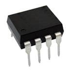
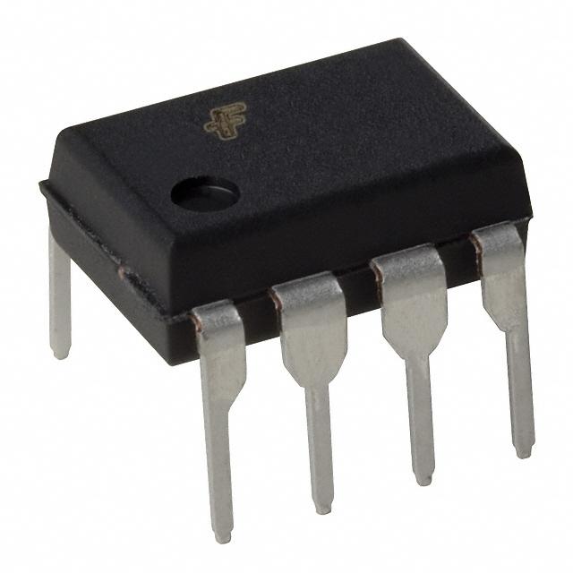
| 产品图片 |
|
| rohs | 符合RoHS无铅 / 符合限制有害物质指令(RoHS)规范要求 |
| 产品系列 | 光耦合器/光电耦合器,高速光耦合器,Avago Technologies HCPL-2430-000E- |
| 数据手册 | http://www.avagotech.com/docs/AV02-0962EN |
| 产品型号 | HCPL-2430-000E |
| PCN封装 | |
| 上升/下降时间(典型值) | 20ns, 10ns |
| 上升时间 | 20 ns |
| 下降时间 | 10 ns |
| 产品目录绘图 |
|
| 产品目录页面 | |
| 产品种类 | 高速光耦合器 |
| 传播延迟tpLH/tpHL(最大值) | 55ns, 55ns |
| 供应商器件封装 | 8-DIP |
| 共模瞬态抗扰度(最小值) | 1kV/µs |
| 其它名称 | 516-1539-5 |
| 包装 | 管件 |
| 商标 | Avago Technologies |
| 安装类型 | 通孔 |
| 封装 | Tube |
| 封装/外壳 | 8-DIP(0.300",7.62mm) |
| 封装/箱体 | PDIP-8 |
| 工作温度 | 0°C ~ 70°C |
| 工厂包装数量 | 50 |
| 数据速率 | 40 MBd |
| 最大功率耗散 | 350 mW |
| 最大反向二极管电压 | 2 V |
| 最大工作温度 | + 70 C |
| 最大正向二极管电压 | 1.5 V |
| 最大正向二极管电流 | 10 mA |
| 最大连续输出电流 | 25 mA |
| 最小工作温度 | 0 C |
| 最小正向二极管电压 | 1.1 V |
| 标准包装 | 50 |
| 每芯片的通道数量 | 2 Channels |
| 电压-正向(Vf)(典型值) | 1.3V |
| 电压-电源 | 4.75 V ~ 5.25 V |
| 电压-隔离 | 3750Vrms |
| 电流-DC正向(If) | 10mA |
| 电流-输出/通道 | 25mA |
| 绝缘电压 | 3750 Vrms |
| 输入-输入侧1/输入侧2 | 2/0 |
| 输入类型 | DC |
| 输出类型 | 推挽式/图腾柱 |
| 输出设备 | Photo IC |
| 通道数 | 2 |


- 商务部:美国ITC正式对集成电路等产品启动337调查
- 曝三星4nm工艺存在良率问题 高通将骁龙8 Gen1或转产台积电
- 太阳诱电将投资9.5亿元在常州建新厂生产MLCC 预计2023年完工
- 英特尔发布欧洲新工厂建设计划 深化IDM 2.0 战略
- 台积电先进制程称霸业界 有大客户加持明年业绩稳了
- 达到5530亿美元!SIA预计今年全球半导体销售额将创下新高
- 英特尔拟将自动驾驶子公司Mobileye上市 估值或超500亿美元
- 三星加码芯片和SET,合并消费电子和移动部门,撤换高东真等 CEO
- 三星电子宣布重大人事变动 还合并消费电子和移动部门
- 海关总署:前11个月进口集成电路产品价值2.52万亿元 增长14.8%


PDF Datasheet 数据手册内容提取
HCPL-2400, HCPL-2430 20 MBd High CMR Logic Gate Optocouplers Data Sheet Lead (Pb) Free RoHS 6 fully compliant RoHS 6 fully compliant options available; -xxxE denotes a lead-free product Description Features The HCPL-2400 and HCPL-2430 high speed opto-cou- • High speed: 40 MBd typical data rate plers combine an 820 nm AlGaAs light emitting diode • High common mode rejection: with a high speed photodetector. This combina-tion re- HCPL-2400: 10 kV/µs at V = 300 V (typical) sults in very high data rate capability and low input cur- CM • AC performance guaranteed over temperature rent. The totem pole output (HCPL-2430) or three state output (HCPL-2400) eliminates the need for a pull up re- • High speed AlGaAs emitter sistor and allows for direct drive of data buses. • Compatible with TTL, STTL, LSTTL, and HCMOS logic The detector has optical receiver input stage with built- families in Schmitt trigger to provide logic compatible wave- • Totem pole and tri state output (no pull up resistor forms, eliminating the need for additional waveshaping. required) The hysteresis provides differential mode noise immuni- • Safety approval ty and minimizes the potential for output signal chatter. – UL recognized – 3750 V rms for 1 minute per The electrical and switching characteristics of the HCPL- UL1577 2400 and HCPL-2430 are guaranteed over the tempera- – IEC/EN/DIN EN 60747-5-2 approved with ture range of 0°C to 70°C. V = 630 V (Option 060) for HCPL-2400 IORM peak Functional Diagram – CSA approved • High power supply noise immunity HCPL-2400/11 HCPL-2430 1 NC VCC 8 ANODE 1 1 8 VCC • MIL-PRF-38534 hermetic version available (HCPL-5400/1 and HCPL-5430/1) 2 7 CATHODE 1 2 7 VO1 Applications 3 6 CATHODE 2 3 6 VO2 • Isolation of high speed logic systems 4 NC 5 ANODE 2 4 5 GND GND • Computer-peripheral interfaces TRUTH TABLE • Switching power supplies (POSITIVE LOGIC) LED ENABLE OUTPUT TRUTH TABLE • Isolated bus driver (networking applications) ON L L (POSITIVE LOGIC) OFF L H LED OUTPUT • Ground loop elimination ON H Z ON L OFF H Z OFF H • High speed disk drive I/O A 0.1 µF bypass capacitor must be connected between pins 5 and 8. • Digital isolation for A/D, D/A conversion • Pulse transformer replacement HCPL-2400 Functional Diagram CAUTION: It is advised that normal static precautions be taken in handling and assembly of this component to prevent damage and/or degradation which may be induced by ESD.
These optocouplers are compatible with TTL, STTL, LSTTL, and HCMOS logic families. When Schottky type TTL devices (STTL) are used, a data rate performance of 20 MBd over temperature is guaranteed when using the application cir- cuit of Figure 13. Typical data rates are 40 MBd. Selection Guide 8-Pin DIP (300 Mil) Minimum CMR Single Dual Minimum Input Maximum Channel Channel dV/dt V On Current Propagation Delay Hermetic CM Package Package (V/µs) (V) (mA) (ns) Package HCPL-2400 1000 300 4 60 HCPL-2430 1000 50 4 60 500 50 6 60 HCPL-540X* 500 50 6 60 HCPL-543X* 500 50 6 60 HCPL-643X* *Technical data for the Hermetic HCPL-5400/01, HCPL-5430/31, and HCPL-6430/31 are on separate Avago publications. Ordering Information HCPL-2400 and HCPL-2430 are UL Recognized with 3750 Vrms for 1 minute per UL1577. Option Part RoHS Non RoHS Surface Gull Tape UL 5000 Vrms/1 IEC/EN/DIN EN number Compliant Compliant Package Mount Wing & Reel Minute rating 60747-5-2 Quantity -000E No option 50 per tube -300E #300 X X 50 per tube HCPL-2400 300mil -500E #500 X X X 1000 per reel DIP-8 -060E #060 X 50 per tube -360E -360 X X X 50 per reel -000E No option 50 per tube -300E #300 X X 50 per tube 300mil HCPL-2430 -500E #500 X X X 1000 per reel DIP-8 -020E - X 50 per tube -060E - X 50 per tube To order, choose a part number from the part number column and combine with the desired option from the option column to form an order entry. Example 1: HCPL-2430-500E to order product of Gull Wing Surface Mount package in Tape in RoHS compliant. Example 2: HCPl-2400 to order product of 8-Pin DIP package in tube packaging and non RoHS compliant. Option datasheets are available. Contact your Avago sales representative or authorized distributor for information. Remarks: The notation ‘#XXX’ is used for existing products, while (new) products launched since 15th July 2001 and RoHS compliant option will use ‘-XXXE‘. 2
Schematic ICC VCC 8 1IF1 IO + VO1 ICC 8 VF1 7 VCC –2 IE 7 2 IF VE ANODE IO 6 + VO VF – CATHODE 3 5GND –3 IO VO2 VF2 6 + 4 IF2 5 GND TRUTH TABLE SHIELD (POSITIVE LOGIC) LED ENABLE OUTPUT TRUTH TABLE ON L L (POSITIVE LOGIC) OFF L H LED OUTPUT ON H Z ON L OFF H Z OFF H HCPL-2400 Schematic 3
Package Outline Drawings 8-Pin DIP Package (HCPL-2400, HCPL-2430) 9.65 ± 0.25 7.62 ± 0.25 (0.380 ± 0.010) (0.300 ± 0.010) TYPE NUMBER 8 7 6 5 OPTION CODE* 6.35 ± 0.25 (0.250 ± 0.010) A XXXXZ DATE CODE YYWWRU UL 1 2 3 4 RECOGNITION 1.78 (0.070) MAX. 1.19 (0.047) MAX. + 0.076 5° TYP. 0.254 - 0.051 + 0.003) 3.56 ± 0.13 4.70 (0.185) MAX. (0.010- 0.002) (0.140 ± 0.005) 0.51 (0.020) MIN. 2.92 (0.115) MIN. DIMENSIONS IN MILLIMETERS AND (INCHES). *MARKING CODE LETTER FOR OPTION NUMBERS. "V" = OPTION 060 OPTION NUMBERS 300 AND 500 NOT MARKED. 1.080 ± 0.320 0.65 (0.025) MAX. (0.043 ± 0.013) NOTE: FLOATING LEAD PROTRUSION IS 0.25 mm (10 mils) MAX. 2.54 ± 0.25 (0.100 ± 0.010) 8-Pin DIP Package with Gull Wing Surface Mount Option 300 (HCPL-2400, HCPL-2430) LAND PATTERN RECOMMENDATION 9.65 ± 0.25 1.016 (0.040) (0.380 ± 0.010) 8 7 6 5 6.350 ± 0.25 10.9 (0.430) (0.250 ± 0.010) 1 2 3 4 2.0 (0.080) 1.27 (0.050) 1.780 9.65 ± 0.25 (0.070) (0.380 ± 0.010) 1.19 MAX. (0.047) 7.62 ± 0.25 MAX. (0.300 ± 0.010) + 0.076 0.254 - 0.051 3.56 ± 0.13 + 0.003) (0.140 ± 0.005) (0.010- 0.002) 1.080 ± 0.320 (0.043 ± 0.013) 0.635 ± 0.25 (0.025 ± 0.010) 12° NOM. 2.54 0.635 ± 0.130 (0.100) (0.025 ± 0.005) BSC DIMENSIONS IN MILLIMETERS (INCHES). LEAD COPLANARITY = 0.10 mm (0.004 INCHES). NOTE: FLOATING LEAD PROTRUSION IS 0.25 mm (10 mils) MAX. 4
Solder Reflow Thermal Profile 300 PREHEATING RATE 3°C + 1°C/–0.5°C/SEC. REFLOW HEATING RATE 2.5°C ± 0.5°C/SEC. PEAK PEAK TEMP. TEMP. 245°C 240°C PEAK TEMP. C) 200 230°C E (° 2.5°C ± 0.5°C/SEC. SOLDERING TUR 116500°°CC S3E0C. 2T0IM0°EC A 140°C PER 3°C + 1°C/–0.5°C S3E0C. M TE 100 PREHEATING TIME 150°C, 90 + 30 SEC. 50 SEC. TIGHT ROOM TYPICAL TEMPERATURE LOOSE 0 0 50 100 150 200 250 TIME (SECONDS) Note: Non-halide flux should be used. Recommended Pb-Free IR Profile TIME WITHIN 5 °C of ACTUAL PEAK TEMPERATURE tp 20-40 SEC. 260 +0/-5 °C Tp 217 °C TL RAMP-UP RE 3 °C/SEC. MAX. RAMP-DOWN ATU Tsmax 150 - 200 °C 6 °C/SEC. MAX. ER Tsmin P TEM PREtHsEAT tL 60 to 150 SEC. 60 to 180 SEC. 25 t 25 °C to PEAK TIME NOTES: THE TIME FROM 25 °C to PEAK TEMPERATURE = 8 MINUTES MAX. Tsmax = 200 °C, Tsmin = 150 °C Note: Non-halide flux should be used. Regulatory Information The HCPL-24XX has been approved by the following organizations: VDE IEC/EN/DIN EN 60747-5-2 Approved according to VDE 0884/06.92 (Option 060 Approved under: only). IEC 60747-5-2:1997 + A1:2002 EN 60747-5-2:2001 + A1:2002 UL DIN EN 60747-5-2 (VDE 0884 Recognized under UL 1577, Component Recognition Teil 2):2003-01. Program, File E55361. (Option 060 only) 5
Insulation and Safety Related Specifications Parameter Symbol Value Units Conditions Minimum External L(101) 7.1 mm Measured from input terminals to output Air Gap (External terminals, shortest distance through air. Clearance) Minimum External L(102) 7.4 mm Measured from input terminals to output Tracking (External terminals, shortest distance path along body. Creepage) Minimum Internal 0.08 mm Through insulation distance, conductor to Plastic Gap conductor, usually the direct distance between the (Internal Clearance) photoemitter and photodetector inside the optocoupler cavity. Tracking Resistance CTI 200 Volts DIN IEC 112/VDE 0303 Part 1 (Comparative Tracking Index) Isolation Group IIIa Material Group (DIN VDE 0110, 1/89, Table 1) Option 300 - surface mount classification is Class A in accordance with CECC 00802. IEC/EN/DIN EN 60747-5-2 Insulation Related Characteristics (HCPL-2400 OPTION 060 ONLY) Description Symbol Characteristic Units Installation classification per DIN VDE 0110/1.89, Table 1 for rated mains voltage ≤300 V rms I-IV for rated mains voltage ≤450 V rms I-III Climatic Classification 55/85/21 Pollution Degree (DIN VDE 0110/1.89) 2 Maximum Working Insulation Voltage V 630 V IORM peak Input to Output Test Voltage, Method b* V x 1.875 = V , 100% Production Test with t = 1 sec, V 1181 V IORM PR m PR peak Partial Discharge < 5 pC Input to Output Test Voltage, Method a* V x 1.5 = V , Type and sample test, V 945 V IORM PR PR peak t = 60 sec, Partial Discharge < 5 pC m Highest Allowable Overvoltage* (Transient Overvoltage, t = 10 sec) V 6000 V ini IOTM peak Safety Limiting Values (Maximum values allowed in the event of a failure, also see Figure 12, Thermal Derating curve.) Case Temperature T 175 °C S Input Current I 230 mA S,INPUT Output Power P 600 mW S,OUTPUT Insulation Resistance at T, V = 500 V R ≥109 Ω S IO S *Refer to the front of the optocoupler section of the current catalog, under Product Safety Regulations section IEC/EN/DIN EN 60747-5-2 for a detailed description. Note: Isolation characteristics are guaranteed only within the safety maximum ratings which must ben ensured by protective circuits in applica- tion. 6
Absolute Maximum Ratings (No derating required up to 70°C) Parameter Symbol Minimum Maximum Units Note Storage Temperature T -55 125 °C S Operating Temperature T -40 85 °C A Average Forward Input Current I 10 mA F(AVG) Peak Forward Input Current I 20 mA 12 FPK Reverse Input Voltage V 2 V R Three State Enable Voltage V -0.5 10 V E (HCPL-2400 Only) Supply Voltage V 0 7 V CC Average Output Collector Current I -25 25 mA O Output Collector Voltage V -0.5 10 V O Output Voltage V -0.5 18 V O Output Collector Power Dissipation P 40 mW O (Each Channel) Total Package Power Dissipation P 350 mW T (Each Channel) Lead Solder Temperature 260°C for 10 sec., 1.6 mm below seating plane (for Through Hole Devices) Reflow Temperature Profile See Package Outline Drawings section (Option #300) Recommended Operating Conditions Parameter Symbol Minimum Maximum Units Power Supply Voltage V 4.75 5.25 V CC Forward Input Current (ON) I 4 8 mA F(ON) Forward Input Voltage (OFF) V 0.8 V F(OFF) Fan Out N 5 TTL Loads Enable Voltage (Low) V 0 0.8 V EL HCPL-2400 Only) Enable Voltage (High) V 2 V V EH CC HCPL-2400 Only) Operating Temperature T 0 70 °C A 7
Electrical Specifications 0°C ≤T ≤70°C, 4.75 V ≤V ≤5.25 V, 4 mA ≤I ≤8 mA, 0 V ≤V ≤0.8 V. All typicals at T = 25°C, V = 5 V, I = 6.0 A CC F(ON) F(OFF) A CC F(ON) mA, V = 0 V, except where noted. See Note 11. F(OFF) Device Parameter Symbol HCPL- Min. Typ.* Max. Units Test Conditions Fig. Note Logic Low Output Voltage V 0.5 V I = 8.0 mA (5 TTL Loads) 1 OL OL Logic High Output V 2.4 V I = -4.0 mA 2 OH OH Voltage 2.7 I = -0.4 mA OH Output Leakage Current I 100 µA V = 5.25 V, V = 0.8 V OHH O F Logic High Enable Current V 2400 2.0 V EH Logic Low Enable Voltage V 2400 0.8 V EL Logic High Enable I 2400 20 µA V = 2.4 V EH E C urrent 100 V = 5.25 V E Logic Low Enable Current I 2400 -0.28 -0.4 mA V = 0.4 V EL E Logic Low Supply Current I 2400 19 26 mA V = 5.25 V, V = 0 V, CCL CC E I = Open O 2430 34 46 V = 5.25 V, I = Open CC O Logic High Supply I 2400 17 26 mA V = 5.25 V, V = 0 V, CCH CC E Current I = Open O 2430 32 42 V = 5.25 V, I = Open CC O High Impedance State I 2400 22 28 mA V = 5.25 V, V = 5.25 V CCZ CC E Supply Current High Impedance State I 2400 20 µA V = 0.4 V V = 2 V OZL O E Output Current I 20 µA V = 2.4 V OZH O I 100 µA V = 5.25 V OZH O Logic Low Short Circuit I 52 mA V = V = 5.25 V, 2 OSL O CC Output Current I = 8 mA F Logic High Short Circuit I -45 mA V = 5.25 V, I = 0 mA, 2 OSH CC F Output Current V = GND O Input Current Hysteresis I 0.25 mA V = 5 V 3 HYS CC Input Forward Voltage V 1.1 1.3 1.5 T = 25°C I = 8 mA F A F 1.0 1.55 4 Input Reverse Breakdown BV 3.0 5.0 V T = 25°C I = 10 µA R A R V oltage 2.0 Temperature ∆V -1.44 mV/°C I = 6 mA 4 F F Coefficient of ∆T Forward Voltage A Input Capacitance C 20 pF f = 1 MHz, V = 0 V IN F *All typical values at T = 25°C and V = 5 V, unless otherwise noted. A CC 8
Switching Specifications 0°C ≤ T ≤ 70°C, 4.75 V ≤ V ≤ 5.25 V, 4 mA ≤ I ≤ 8 mA, 0 V ≤ V ≤ 0.8 V. All typicals at T = 25°C, V = 5 V, A CC F(ON) F(OFF) A CC I = 6.0 mA, V = 0 V, except where noted. See Note 11. F(ON) F(OFF) Device Parameter Symbol HCPL- Min. Typ.* Max. Units Test Conditions Figure Note Propagation Delay t 55 ns I = 7 mA 5, 6, 7 1, 4, PHL F(ON) Time to Logic Low 5, 6 Output Level 15 33 60 Propagation Delay t 55 ns I = 7 mA 5, 6, 7 1, 4, PLH F(ON) Time to Logic High 5, 6 Output Level 15 30 60 Pulse Width |t -t | 2 15 ns I = 7 mA 5, 8 6 PHL PLH F(ON) Distortion 5 25 Propagation Delay t 35 ns Per Notes & Text 15, 16 7 PSK Skew Output Rise Time t 20 ns 5 r Output Fall Time t 10 ns 5 f Output Enable Time t 2400 15 ns 9, 10 PZH to Logic High Output Enable Time t 2400 30 ns 9, 10 PZL to Logic Low Output Disable Time t 2400 20 ns 9, 10 PHZ from Logic High Output Disable Time t 2400 15 ns 9, 10 PLZ from Logic Low Logic High Common |CM | 1000 10,000 V/µs V = 300 V, T = 25°C, 11 9 H CM A Mode Transient I = 0 mA F Immunity Logic Low Common |CM| 1000 10,000 V/µs V = 300 V, T = 25°C, 11 9 L CM A Mode Transient I = 4 mA F Immunity Power Supply Noise PSNI 0.5 V V = 5.0 V, 10 p-p CC Immunity 48 Hz ≤ = F ≤50 MHz AC *All typical values at T = 25°C and V = 5 V, unless otherwise noted. A CC 9
Package Characteristics Parameter Sym. Device Min. Typ.* Max. Units Test Conditions Fig. Note Input-Output V 3750 V rms RH ≤50%, 3, 13 ISO Momentary t = 1 min., Withstand Voltage** T = 25°C A Input-Output R 1012 Ω V = 500 Vdc 3 I-O I-O Resistance Input-Output C 0.6 pF f = 1 MHz I-O Capacitance V = 0 Vdc I-O Input-Input I 2430 0.005 µA RH ≤45% 8 I-I Insulation Leakage t = 5 s, Current V = 500 Vdc I-I Resistance R 2430 1011 Ω V = 500 Vdc 8 I-I I-I (Input-Input) Capacitance C 2430 0.25 pF f = 1 MHz 8 I-I (Input-Input) *All typical values are at T = 25°C. A **The Input-Output Momentary Withstand Voltage is a dielectric voltage rating that should not be interpreted as an input-output continuous voltage rating. For the continuous voltage rating refer to the VDE 0884 Insulation Related Characteristics Table (if applicable), your equipment lev- el safety specification or Avago Application Note 1074 entitled “Optocoupler Input-Output Endurance Voltage,” publication number 5963-2203E. Notes: 1. Each channel. 2. Duration of output short circuit time not to exceed 10 ms. 3. Device considered a two terminal device: pins 1, 2, 3, and 4 shorted together, and pins 5, 6, 7, and 8 shorted together. 4. t propagation delay is measured from the 50% level on the rising edge of the input current pulse to the 1.5 V level on the falling edge of the PHL output pulse. The t propagation delay is measured from the 50% level on the falling edge of the input current pulse to the 1.5 V level on the PLH rising edge of the output pulse. 5. The typical data shown is indicative of what can be expected using the application circuit in Figure 13. 6. This specification simulates the worst case operating conditions of the HCPL-2400 over the recommended operating temperature and V range CC with the suggested application circuit of Figure 13. 7. Propagation delay skew is discussed later in this data sheet. 8. Measured between pins 1 and 2 shorted together, and pins 3 and 4 shorted together. 9. Common mode transient immunity in a Logic High level is the maximum tolerable (positive) dV /dt of the common mode pulse, V , to assure CM CM that the output will remain in a Logic High state (i.e., V > 2.0 V). Common mode transient immunity in a Logic Low level is the maximum toler- O able (negative) dV /dt of the common mode pulse, V , to assure that the output will remain in a Logic Low state (i.e., V < 0.8 V). CM CM O 10. Power Supply Noise Immunity is the peak to peak amplitude of the ac ripple voltage on the V line that the device will withstand and still remain CC in the desired logic state. For desired logic high state, V > 2.0 V, and for desired logic low state, V < 0.8 V. OH(MIN) OL(MAX) 11. Use of a 0.1 µF bypass capacitor connected between pins 8 and 5 adjacent to the device is required. 12. Peak Forward Input Current pulse width < 50 µs at 1 KHz maximum repetition rate. 13. In accordance with UL 1577, each optocoupler is proof tested by applying an insulation test voltage ≥ 4500 V rms for one second (leakage detec- tion current limit, I ≤ 5 µA). This test is performed before the 100% Production test shown in the IEC/EN/DIN EN 60747-5-2 Insulation Related I-O Characteristics Table, if applicable. 10
Figure 1. Typical logic low output voltage vs. logic low Figure 2. Typical logic high output voltage vs. logic Figure 3. Typical output voltage vs. input forward output current. high output current. current. Figure 4. Typical diode input forward current charac- Figure 5. Test circuit for t , t , t, and t. PLH PHL r f teristic. Figure 6. Typical propagation delay vs. ambient Figure 7. Typical propagation delay vs. input forward Figure 8. Typical pulse width distortion vs. ambient temperature. current. temperature. 11
Figure 9. Test circuit for t , t , t and t . Figure 10. Typical enable propagation delay vs. ambi- PHZ PZH PLZ PZL ent temperature. HCPL-2400/11 VCC 1 NC VCC 8 IF 0.1 µF * B 2 7 3 6 OUTPUT VO + A MONITORING NODE VF–F 4 NC GND 5 †C L = 15 pF – IS 800 VCM NT PS (mW) + – RE 700 IS (mA) PULSE GENERATOR R U 600 C T U 500 P N , IS 400 P – 300 HCPL-2400 fig 11a ER W 200 O T P 100 U TP 0 U 0 25 50 75 100 125 150 175 200 O TS – CASE TEMPERATURE – °C Figure 11. Test diagram for common mode transient immunity and typical waveforms. Figure 12. Thermal derating curve, dependence of safety limiting value with case temperature per IEC/EN/DIN EN 60747-5-2. HCPL-2400 fig 12 12
Applications Figure 13. Recommended 20 MBd HCPL-2400/30 interface circuit. Figure 14. Alternative HCPL-2400/30 interface circuit. DATA IF 50% INPUTS CLOCK VO 1.5 V IF 50% DATA OUTPUTS tPSK VO 1.5 V CLOCK tPSK tPSK Figure 15. Illustration of propagation delay skew – t . Figure 16. Parallel data transmission example. PSK HCPL-2400 fig 15 HCPL-2400 fig 16 Figure 17. Modulation code selections. Figure 18. Typical HCPL-2400/30 output schematic. 13
Propagation Delay, Pulse-Width Distortion and Propa- Propagation delay skew represents the uncertainty of gation Delay Skew where an edge might be after being sent through an optocoupler. Figure 16 shows that there will be uncer- Propagation delay is a figure of merit which describes tainty in both the data and the clock lines. It is impor- how quickly a logic signal propagates through a sys- tant that these two areas of uncertainty not overlap, tem. The propagation delay from low to high (t ) is the otherwise the clock signal might arrive before all of the PLH amount of time required for an input signal to propa- data outputs have settled, or some of the data outputs gate to the output, causing the output to change from may start to change before the clock signal has arrived. low to high. Similarly, the propagation delay from high From these considerations, the absolute minimum pulse to low (t ) is the amount of time required for the input width that can be sent through optocouplers in a par- PHL signal to propagate to the output, causing the output to allel application is twice t . A cautious design should PHZ change from high to low (see Figure 5). use a slightly longer pulse width to ensure that any addi- tional uncertainty in the rest of the circuit does not cause Pulse-width distortion (PWD) results when t and t PLH PHL a problem. differ in value. PWD is defined as the difference between t and t and often determines the maximum data The HCPL-2400/30 optocouplers offer the advantages of PLH PHL rate capability of a transmission system. PWD can be ex- guaranteed specifications for propagation delays, pulse- pressed in percent by dividing the PWD (in ns) by the width distortion, and propagation delay skew over the minimum pulse width (in ns) being transmitted. Typi- recommended temperature, input current, and power cally, PWD on the order of 20-30% of the minimum pulse supply ranges. width is tolerable; the exact figure depends on the par- Application Circuit ticular application (RS232, RS422, T-1, etc.). A recommended LED drive circuit is shown in Figure 13. Propagation delay skew, t , is an important param- PSK This circuit utilizes several techniques to minimize the eter to consider in parallel data applications where total pulse-width distortion at the output of the opto- synchronization of signals on parallel data lines is a con- coupler. By using two inverting TTL gates connected in cern. If the parallel data is being sent through a group series, the inherent pulse-width distortion of each gate of optocouplers, differences in propagation delays will cancels the distortion of the other gate. For best results, cause the data to arrive at the outputs of the optocou- the two series-connected gates should be from the same plers at different times. If this difference in propagation package. delays is large enough, it will determine the maximum rate at which parallel data can be sent through the op- The circuit in Figure 13 also uses techniques known as tocouplers. prebias and peaking to enhance the performance of the optocoupler LED. Prebias is a small forward voltage ap- Propagation delay skew is defined as the difference be- plied to the LED when the LED is off. This small prebias tween the minimum and maximum propagation delays, voltage partially charges the junction capacitance of the either t or t , for any given group of optocouplers PLH PHL LED, allowing the LED to turn on more quickly. The speed which are operating under the same conditions (i.e., the of the LED is further increased by applying momentary same drive current, supply voltage, output load, and op- current peaks to the LED during the turn-on and turn-off erating temperature). As illustrated in Figure 15, if the in- transitions of the drive current. These peak currents help puts of a group of optocouplers are switched either ON to charge and discharge the capacitances of the LED or OFF at the same time, t is the difference between PSK more quickly, shortening the time required for the LED the shortest propagation delay, either t or t , and the PLH PHL to turn on and off. longest pro-pagation delay, either t or t . PLH PHL As mentioned earlier, t can determine the maximum PSK parallel data transmission rate. Figure 16 is the timing diagram of a typical parallel data application with both the clock and the data lines being sent through opto- couplers. The figure shows data and clock signals at the inputs and outputs of the optocouplers. To obtain the maximum data transmission rate, both edges of the clock signals are being used to clock the data; if only one edge were used, the clock signal would need to be twice as fast.
Switching performance of the HCPL-2400/30 optocou- the output of the optocoupler, but will not necessarily plers is not sensitive to the TTL logic family used in the result in lower pulse-width distortion or propagation de- recommended drive circuit. The typical and worst-case lay skew. This reduction in overall propagation delay is switching parameters given in the data sheet can be due to shorter delays in the drive circuit, not to changes met using common 74LS TTL inverting gates or buffers. in the propagation delays of the optocoupler; optocou- Use of faster TTL families will slightly reduce the overall pler propagation delays are not affected by the speed of propagation delays from the input of the drive circuit to the logic used in the drive circuit. For product information and a complete list of distributors, please go to our website: www.avagotech.com Avago, Avago Technologies, and the A logo are trademarks of Avago Technologies Limited in the United States and other countries. Data subject to change. Copyright © 2007 Avago Technologies Limited. All rights reserved. Obsoletes AV01-0563EN AV02-0962EN - January 4, 2008
Mouser Electronics Authorized Distributor Click to View Pricing, Inventory, Delivery & Lifecycle Information: B roadcom Limited: HCPL-2430-000E HCPL-2430-020E HCPL-2430-060E HCPL-2430-300E HCPL-2430-500E