ICGOO在线商城 > GQM22M5C2H270GB01L
 Datasheet下载
- 型号: GQM22M5C2H270GB01L
- 制造商: Murata
- 库位|库存: xxxx|xxxx
- 要求:
| 数量阶梯 | 香港交货 | 国内含税 |
| +xxxx | $xxxx | ¥xxxx |
查看当月历史价格
查看今年历史价格
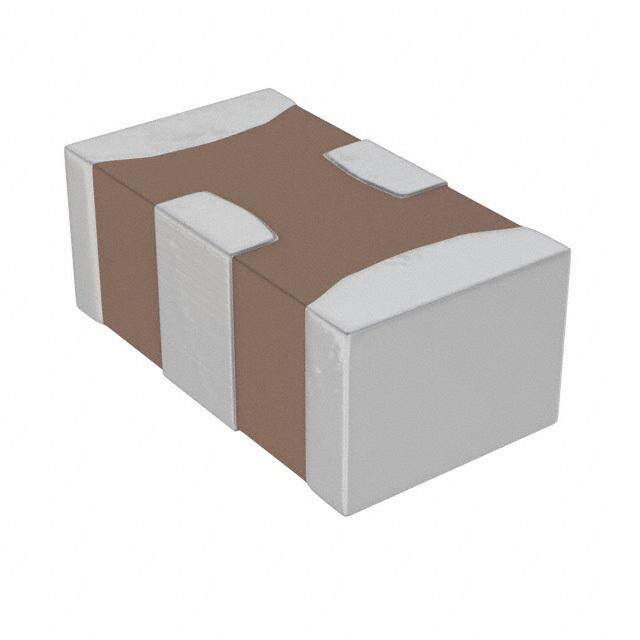
GQM22M5C2H270GB01L产品简介:
ICGOO电子元器件商城为您提供GQM22M5C2H270GB01L由Murata设计生产,在icgoo商城现货销售,并且可以通过原厂、代理商等渠道进行代购。 提供GQM22M5C2H270GB01L价格参考¥12.69-¥31.21以及MurataGQM22M5C2H270GB01L封装/规格参数等产品信息。 你可以下载GQM22M5C2H270GB01L参考资料、Datasheet数据手册功能说明书, 资料中有GQM22M5C2H270GB01L详细功能的应用电路图电压和使用方法及教程。
| 参数 | 数值 |
| 产品目录 | |
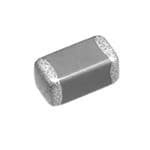
| 描述 | CAP CER 27PF 500V 2% NP0 1111多层陶瓷电容器MLCC - SMD/SMT 1111 C0G 500V 27pF |
| 产品分类 | |
| 品牌 | Murata Electronics North America |
| 产品手册 | |
| 产品图片 |
|
| rohs | 符合RoHS无铅 / 符合限制有害物质指令(RoHS)规范要求 |
| 产品系列 | MLCC,多层陶瓷电容器MLCC - SMD/SMT,Murata Electronics GQM22M5C2H270GB01LGQM |
| 数据手册 | |
| 产品型号 | GQM22M5C2H270GB01L |
| 产品 | High Q MLCCs |
| 产品目录绘图 |
|
| 产品种类 | 多层陶瓷电容器MLCC - SMD/SMT |
| 其它名称 | 490-8585-6 |
| 包装 | Digi-Reel® |
| 厚度(最大值) | 0.053"(1.35mm) |
| 商标 | Murata Electronics |
| 外壳代码-in | 1111 |
| 外壳代码-mm | 2828 |
| 外壳宽度 | 2.8 mm |
| 外壳长度 | 2.8 mm |
| 外壳高度 | 1.15 mm |
| 大小/尺寸 | 0.110" 长 x 0.110" 宽(2.80mm x 2.80mm) |
| 安装类型 | 表面贴装,MLCC |
| 容差 | ±2% |
| 封装 | Reel |
| 封装/外壳 | 1111(2828 公制) |
| 封装/箱体 | 1111 (2828 metric) |
| 工作温度 | -55°C ~ 125°C |
| 工作温度范围 | - 55 C to + 125 C |
| 工厂包装数量 | 1000 |
| 应用 | RF,微波,高频 |
| 引线形式 | - |
| 引线间距 | - |
| 最大工作温度 | + 125 C |
| 最小工作温度 | - 55 C |
| 标准包装 | 1 |
| 温度系数 | C0G,NP0 |
| 温度系数/代码 | +/- 30 PPM / C |
| 特性 | 高 Q 值,低损耗 |
| 特色产品 | http://www.digikey.com/cn/zh/ph/Murata/Caps.html |
| 电介质 | C0G (NP0) |
| 电压-额定 | 500V |
| 电压额定值 | 500 V |
| 电压额定值DC | 500 V |
| 电容 | 27pF |
| 端接类型 | SMD/SMT |
| 等级 | - |
| 类型 | High Frequency High Q Type |
| 系列 | GQM |
| 高度-安装(最大值) | - |

.jpg)


- 商务部:美国ITC正式对集成电路等产品启动337调查
- 曝三星4nm工艺存在良率问题 高通将骁龙8 Gen1或转产台积电
- 太阳诱电将投资9.5亿元在常州建新厂生产MLCC 预计2023年完工
- 英特尔发布欧洲新工厂建设计划 深化IDM 2.0 战略
- 台积电先进制程称霸业界 有大客户加持明年业绩稳了
- 达到5530亿美元!SIA预计今年全球半导体销售额将创下新高
- 英特尔拟将自动驾驶子公司Mobileye上市 估值或超500亿美元
- 三星加码芯片和SET,合并消费电子和移动部门,撤换高东真等 CEO
- 三星电子宣布重大人事变动 还合并消费电子和移动部门
- 海关总署:前11个月进口集成电路产品价值2.52万亿元 增长14.8%


PDF Datasheet 数据手册内容提取
C02E.pdf Nov.27,2017 Chip Multilayer Ceramic Capacitors for General 2018
!Note (cid:129) Please read rating and !CAUTION (for storage, operating, rating, soldering, mounting and handling) in this catalog to prevent smoking and/or burning, etc. C02E.pdf (cid:129) This catalog has only typical specifications. Therefore, please approve our product specifications or transact the approval sheet for product specifications before ordering. Nov.27,2017 Explanation of Symbols in This Catalog WEB Links are provided to the latest information from the PDF version of the catalog, which is available on the web. For applications that do not require the particular reliability such as Derating 1 the general equipment This product is suitable when a voltage continuously applied to a capacitor in an operating circuit, is used below (derated) the rated voltage of the capacitor. This model guarantees the test conditions in Infotainment for Automotive the endurance test, at a rated voltage x 100% at the maximum The product for entertainment equipment like car navigations, car operating temperature. A reliability assurance level equivalent to a audios, and body control equipment like wipers, power windows. common product can be secured, by using this product within the voltage and temperature derated conditions recommended in the Powertrain/Safety for Automotive figure below. Product used for applications (running, turning, stopping and safety devices) which particularly concern human life, such as in devices for Recommended Conditions of the Derating Operating Voltage and Temperature automobiles. %)120 MTheedsieca pl-rogdraudcet sp arored uincttesn fdoer dIm foprl aunstee idn Mimepdliacnatl eDde mviceedsical devices Voltage (100 125°C Type sgT*u1ah cseNhtyor iaancsr- e eccl raesiturciditctriaaaolbcs c ltpeiirma cfcouuerilt maustsaoekr sein.r sn,o cno-cchrlietiacra ilm ciprclaunittss., *i1nsulin pumps and Voltage/Rated 486000 18055°C°C T yTpyepe Tnenohdtis ad tniergeremcrt ltryhe lfeien lrkisfee td oo t fc oti rhlciefue pi tsasut ipinep niomtr stp,hl aio.enu.t lcedid rtc hmueie tfdsu intchcaatl itdo wenvailillci tneyos o tt fhd tairhtee ca trely Operating 200 device be reduced or halted by failure of the circuit. 0 25 50 75 100 125 150 Product Temperature (°C) AEC-Q200 compliant product Derating 2 When the product temperature exceeds 105°C, please use this product within the voltage and temperature derated conditions in the Safety Standard Certified Product figure below. Products that acquired safety standard certification IEC60384-14 and products based on the Electrical Appliance and Material Safety 700 Law of Japan. Rated Voltage 630V %) 600 LBdBPsaoiryasofw sseddei tepuddyvaci soilttsasinsoiwin p nttga hh o itacsefi et o aJE rnacalae rhpfmecoiae tribncrv hai. ecmsidagea lhid nAt f e orpfrernpieaq ltqiluahsue neaenc nencedlcye a yecn ltbedraic cMntadralos tad eoperfp i maVlilaH aSntFace,f erUei ataHylnsF d,L ala omnwwda otef rJiaalp an oltage/Rated Voltage ( ((434355500000000VV)) Rated Voltage 450V microwave or beyond. ng V 200 LTohwis cinadpuacctiatonrc ies designed so that the parasitic inductance Operati 100 component (ESL) that the capacitor has on the high frequency side becomes lower. 0 0 25 50 75 100 125 150 Fail safe product Product Temperature (°C) This capacitor is designed to prevent failures as much as possible by Derating 3 short mode. Please apply the derating curve according to the operating temperature. Product resistant to deflection cracking Please refer to detailed specifications sheet for details. This capacitor is designed to prevent failures as much as possible by short mode caused by cracking when there is board deflection. Derating 4 When the product temperature exceeds 125°C, please use this Product with solder cracking suppression product within the voltage and temperature derated conditions in the “This capacitor is configured with metal terminals and leads figure below. connected to the chip. The metal terminals and leads relieve the stress from expansion and contraction of the solder, to suppress %) 120 PTccsoeohrolrnidsadfi empugrrcu icoctrrd acsautuacicoipkttnaia ns.cbguilt.ep”o pfror iesr s auscseoesud as, ctboiycu dnseotivicsi esni onreigsd etuh, cwet ihmoinca htae nordciac lluosr wasn dwdish teonr taio n Voltage/Rated Voltage ( 1(0486500000) NPalooul myDmiCne ubrmi ac sao pcxahidcaiizrtaeocdr t ifies rlnmisot ficcoasrp daiecliteacntrciec .change with DC bias due to Operating 200-75 -50 -25 0 25 50 75 100 125 150 175 Product Temperature (°C) Low-inductance product suitable for noise suppression. This product has extremely low ESL and is suitable for suppression Derating 5 of noise, including high frequencies. Please apply the rated voltage derating over 150 °C. This product can also be used as a low-ESL, high-performance Please refer to detailed specifications sheet for details. bypass capacitor. Product for bonding Since gold is used for the external electrodes, the capacitor can be mounted by die bonding/wire bonding. 2
!Note (cid:129) Please read rating and !CAUTION (for storage, operating, rating, soldering, mounting and handling) in this catalog to prevent smoking and/or burning, etc. C02E.pdf (cid:129) This catalog has only typical specifications. Therefore, please approve our product specifications or transact the approval sheet for product specifications before ordering. Nov.27,2017 Selection Guide for Capacitors For general Infotainment for automotive SMD SMD Solder mounting Solder mounting Chip type Chip type GRM p40 GRT WEB GRM For LCD backlight inverter circuit WEB only GR3 High effective capacitance & p109 Powertrain/Safety for automotive high ripple current GRJ Soft termination p120 SMD GXM WEB Solder mounting GR4 For information devices only p125 Chip type GR7 For camera flash circuit only p130 GCM WEB GJM p135 GC3 High effective capacitance & WEB high ripple current GQM High power p164 GCJ Soft termination WEB GA2 Based on the Electrical Appliance p184 GGM WEB and Material Safety Law of Japan GA3 p189 GCQ WEB LLL LW reversed p219 GCD MLSC design WEB LLA 8 terminals p222 GCE Soft termination MLSC design WEB LLM 10 terminals p228 GGD MLSC design WEB LLR LW reversed controlled ESR p232 NFM 3 terminals WEB NFM 3 terminals p236 Metal terminal type GJ4 Low distortion WEB KCM WEB GJ8 Low acoustic noise WEB KC3 Hhiigghh reipffpelcet civuer rceanptacitance & WEB On interposer board KCA WEB ZRA WEB Limited to Conductive Glue Mounting ZRB WEB Chip type Metal terminal type GCB Ni plating + Pd plating termination WEB conductive glue mounting KRM p239 GCG AgPd termination conductive glue WEB mounting KR3 High effective capacitance & p243 Lead type high ripple current Resin molding SMD type Solder mounting DK1 WEB RCE WEB Wire bonding mounting RHE 150°C operation leaded WEB Chip type RHS 200°C operation leaded WEB GMA Microchip p249 DE6 WEB GMD p256 Lead type Medical-grade products for implanted medical devices Solder mounting SMD RDE WEB Solder mounting DEH High temperature low loss WEB Chip type DEA High temperature Class 1 WEB GCH WEB DEB Class 2 WEB DEC WEB DEF For LCD backlight inverter circuit WEB only DHR WEB DEJ Based on the Electrical Appliance WEB and Material Safety Law of Japan DE1 X1/Y1 Class certified product WEB DE2 X1/Y2 Class certified product WEB Screw termination mounting DHS WEB DHK High voltage AC rated WEB 3
!Note (cid:129) Please read rating and !CAUTION (for storage, operating, rating, soldering, mounting and handling) in this catalog to prevent smoking and/or burning, etc. C02E.pdf (cid:129) This catalog has only typical specifications. Therefore, please approve our product specifications or transact the approval sheet for product specifications before ordering. Nov.27,2017 o Part Numbering WEB Chip Multilayer Ceramic Capacitors for General (Part Number) GR M 18 8 B1 1H 102 K A01 D 1 2 3 4 5 6 7 8 9 : 1Product ID 2Series Product ID Code Series 2 Based on the Electrical Appliance and Material Safety Law of Japan Chip Multilayer Ceramic Capacitors for General Purpose GA 3 Safety Standard Certified Chip Multilayer Ceramic Capacitors for General Purpose GJ M High Q Chip Multilayer Ceramic Capacitors for General Purpose A Wire Bonding Mount Multilayer Microchip Capacitors for General Purpose GM D Wire Bonding/AuSn Soldering Mount Chip Multilayer Ceramic Capacitors for General Purpose GQ M High Q and High Power Chip Multilayer Ceramic Capacitors for General Purpose 3 High Effective Capacitance & High Ripple Current Chip Multilayer Ceramic Capacitors for General Purpose 4 Chip Multilayer Ceramic Capacitors for Camera Flash Circuit only GR 7 Chip Multilayer Ceramic Capacitors for Ethernet LAN and Primary-secondary Coupling of DC-DC Converters J Soft Termination Chip Multilayer Ceramic Capacitors for General Purpose M Chip Multilayer Ceramic Capacitors for General Purpose 3 High Effective Capacitance & High Allowable Ripple Current Metal Terminal Type Multilayer Ceramic Capacitors for General Purpose KR M Metal Terminal Type Multilayer Ceramic Capacitors for General Purpose A 8 Terminals Low ESL Chip Multilayer Ceramic Capacitors for General Purpose L LW Reversed Low ESL Chip Multilayer Ceramic Capacitors for General Purpose LL M 10 Terminals Low ESL Chip Multilayer Ceramic Capacitors for General Purpose R LW Reversed Controlled ESR Low ESL Chip Multilayer Ceramic Capacitors for General Purpose 3Chip Dimensions (LxW) Code Dimensions (LxW) EIA 02 0.4x0.2mm 01005 0D 0.38x0.38mm 015015 03 0.6x0.3mm 0201 05 0.5x0.5mm 0202 08 0.8x0.8mm 0303 1U 0.6x1.0mm 02404 15 1.0x0.5mm 0402 18 1.6x0.8mm 0603 21 2.0x1.25mm 0805 22 2.8x2.8mm 1111 31 3.2x1.6mm 1206 32 3.2x2.5mm 1210 42 4.5x2.0mm 1808 43 4.5x3.2mm 1812 52 5.7x2.8mm 2211 55 5.7x5.0mm 2220 Continued on the following page. 5
!Note (cid:129) Please read rating and !CAUTION (for storage, operating, rating, soldering, mounting and handling) in this catalog to prevent smoking and/or burning, etc. C02E.pdf (cid:129) This catalog has only typical specifications. Therefore, please approve our product specifications or transact the approval sheet for product specifications before ordering. Nov.27,2017 (Part Number) GR M 18 8 B1 1H 102 K A01 D 1 2 3 4 5 6 7 8 9 : Continued from the preceding page. 4Height Dimension (T) (Except KRp) 4Height Dimension (T) (KRp Only) Code Dimension (T) Code Dimension (T) 2 0.2mm E 1.8mm 3 0.3mm F 1.9mm 4 0.4mm K 2.7mm 5 0.5mm L 2.8mm 6 0.6mm Q 3.7mm 7 0.7mm T 4.8mm 8 0.8mm W 6.4mm 9 0.85mm A 1.0mm B 1.25mm C 1.6mm D 2.0mm E 2.5mm M 1.15mm Q 1.5mm X Depends on individual standards. 5Temperature Characteristics Temperature Temperature Characteristics Capacitance Change Each Temperature (%) Characteristic Codes Operating Code Public Reference Temperature Caopra Tcietmanpceer aCthuarenge TemRpaenrgaeture –55°C *6 –10°C STD Code Temperature Range Coefficient Max. Min. Max. Min. Max. Min. 1X SL JIS 20°C 20 to 85°C +350 to –1000ppm/°C –55 to 125°C - - - - - - 2C CH JIS 20°C 20 to 125°C 0±60ppm/°C –55 to 125°C 0.82 –0.45 0.49 –0.27 0.33 –0.18 3C CJ JIS 20°C 20 to 125°C 0±120ppm/°C –55 to 125°C 1.37 –0.9 0.82 –0.54 0.55 –0.36 3U UJ JIS 20°C 20 to 85°C –750±120ppm/°C –25 to 85°C - - 4.94 2.84 3.29 1.89 4C CK JIS 20°C 20 to 125°C 0±250ppm/°C –55 to 125°C 2.56 –1.88 1.54 –1.13 1.02 –0.75 5C C0G EIA 25°C 25 to 125°C 0±30ppm/°C –55 to 125°C 0.58 –0.24 0.4 –0.17 0.25 –0.11 5G X8G *2 25°C 25 to 150°C 0±30ppm/°C –55 to 150°C 0.58 –0.24 0.4 –0.17 0.25 –0.11 7U U2J EIA 25°C 25 to 125°C *3 –750±120ppm/°C –55 to 125°C 8.78 5.04 6.04 3.47 3.84 2.21 B1 B *1 JIS 20°C –25 to 85°C ±10% –25 to 85°C - - - - - - B3 B JIS 20°C –25 to 85°C ±10% –25 to 85°C - - - - - - C7 X7S EIA 25°C –55 to 125°C ±22% –55 to 125°C - - - - - - C8 X6S EIA 25°C –55 to 105°C ±22% –55 to 105°C - - - - - - D7 X7T EIA 25°C –55 to 125°C +22%, –33% –55 to 125°C - - - - - - D8 X6T EIA 25°C –55 to 105°C +22%, –33% –55 to 105°C - - - - - - E7 X7U EIA 25°C –55 to 125°C +22%, –56% –55 to 125°C - - - - - - R1 R *1 JIS 20°C –55 to 125°C ±15% –55 to 125°C - - - - - - R6 X5R EIA 25°C –55 to 85°C ±15% –55 to 85°C - - - - - - R7 X7R EIA 25°C –55 to 125°C ±15% –55 to 125°C - - - - - - ±10% *4 - - - - - - W0 X7T EIA 25°C –55 to 125°C –55 to 125°C +22%, –33% *5 - - - - - - *1 Capacitance change is specified with 50% rated voltage applied. *2 Murata Temperature Characteristic Code. *3 Rated Voltage 100Vdc max: 25 to 85°C *4 Apply DC350V bias. *5 No DC bias. *6 –25°C (Reference Temperature 20°C) / –30°C (Reference Temperature 25°C) Continued on the following page. 6
!Note (cid:129) Please read rating and !CAUTION (for storage, operating, rating, soldering, mounting and handling) in this catalog to prevent smoking and/or burning, etc. C02E.pdf (cid:129) This catalog has only typical specifications. Therefore, please approve our product specifications or transact the approval sheet for product specifications before ordering. Nov.27,2017 (Part Number) GR M 18 8 B1 1H 102 K A01 D 1 2 3 4 5 6 7 8 9 : Continued from the preceding page. 6Rated Voltage 8Capacitance Tolerance Code Rated Voltage Code Capacitance Tolerance 0E DC2.5V B ±0.1pF 0G DC4V C ±0.25pF 0J DC6.3V ±0.5pF (Less than 10pF) D 1A DC10V ±0.5% (10pF and over) 1C DC16V F ±1% 1E DC25V G ±2% 1H DC50V J ±5% 1J DC63V K ±10% 1K DC80V M ±20% 2A DC100V W ±0.05pF 2D DC200V 2E DC250V 9Individual Specification Code (Except LLR) 2W DC450V Expressed by three figures. 2H DC500V 2J DC630V 9ESR (LLR Only) 3A DC1kV Code ESR 3D DC2kV E01 100mΩ 3F DC3.15kV E03 220mΩ BB DC350V E05 470mΩ E2 AC250V E07 1000mΩ GB X2; AC250V (Safety Standard Certified Type GB) GD Y3; AC250V (Safety Standard Certified Type GD) :Packaging GF Y2, X1/Y2; AC250V (Safety Standard Certified Type GF) Code Packaging YA DC35V L ø180mm Embossed Taping D/E/W ø180mm Paper Taping 7Capacitance K ø330mm Embossed Taping Expressed by three-digit alphanumerics. The unit is picofarad (pF). J/F ø330mm Paper Taping The first and second figures are significant digits, and the third figure expresses the number of zeros which follow the two T Bulk Tray numbers. If there is a decimal point, it is expressed by the capital letter "R." In this case, all figures are significant digits. If any alphabet, other than "R", is included, this indicates the specific part number is a non-standard part. Ex.) Code Capacitance R50 0.50pF 1R0 1.0pF 100 10pF 103 10000pF Please contact us if you find any part number not provided in this table. 7
!Note • Please read rating and !CAUTION (for storage, operating, rating, soldering, mounting and handling) in this catalog to prevent smoking and/or burning, etc. C02E.pdf • This catalog has only typical specifications. Therefore, please approve our product specifications or transact the approval sheet for product specifications before ordering. Nov.27,2017 M R G High Q and High Power Chip Multilayer Ceramic Capacitors for General Purpose GQM Series 3 WEB R G J R High Frequency Capacitor Ideal for PA Design of Base Stations G 4 R G Features 7 R 1 Mainly ideal for base stations of mobile communication devices and temperature compensation G of related modules. M J This product is ideal for temperature compensation of high frequency circuits, such as resonant circuits, G tuning circuits, and impedance matching circuits where the operating characteristics of the device are greatly affected by the capacitance fluctuation. M Q G Ceramic Internal Electrodes (Cu) 2 Ni/Sn Plated Layer A G Foundation Electrode Layer 3 GAGB <Example of Structure> 2 High Q and low ESR in VHF, UHF and microwave frequency bands. 3 GAGD High Q and low ESR were achieved at a high frequency by adopting ceramic material as the dielectric material which enables an extremely low loss at high frequency, and base metal electrodes as the internal electrodes. 3 A GGF 10000 1000 New Material GQM New Material GQM Conventional Material GRM Conventional Material GRM 1608 (in mm)/0603 (in inch)/10pF/50V 1000 1608 (in mm)/0603 (in inch)/10pF/50V LL 100 L Q100 Q A 10 L L 10 M 1 1 L 0 500 1000 1500 2000 2500 3000 100 200 300 400 500 600 700 L Frequency (MHz) Frequency (MHz) <Comparison between Q - Frequency Characteristics> <Comparison between Q - Frequency Characteristics> R L L 3 Can be used for tight tolerance. M F In addition to standard tolerance, the allowable range of this product is also suitable for the following narrow tolerance. N Standard Capacitance Tolerance Narrow Capacitance Tolerance Capacitance Range M (Capacitance Tolerance Symbol) (Capacitance Tolerance Symbol) R K to 0.9pF ±0.1pF (B) ±0.05pF (W) 1.0 to 5.0pF ±0.25pF (C) ±0.05pF (W), ±0.1pF (B) 3 5.1 to 9.9pF ±0.5pF (D) ±0.05pF (W), ±0.1pF (B), ±0.25pF (C) R K 10pF to ±5% (J) ±2% (G) A M Specifications G D e g e M Size (mm) 1.0×0.5mm to 2.8×2.8mm G n Rated Voltage 50Vdc to 500Vdc T o Cautiotice Capacitance 0.10pF to 510pF !/N L W Main Applications Measuring instruments, other ultra compact/thin devices <Dimensions> This catalog contains only a portion of the product lineup. Please refer to the capacitor search tool on the Murata Web site for details. 164
!Note • Please read rating and !CAUTION (for storage, operating, rating, soldering, mounting and handling) in this catalog to prevent smoking and/or burning, etc. C02E.pdf • This catalog has only typical specifications. Therefore, please approve our product specifications or transact the approval sheet for product specifications before ordering. Nov.27,2017 M GQM Series Temperature Compensating Type Part Number List R G 3 T Rated TC R 1.0×0.5mm Cap. Tol. Part Number p* G max. Voltage Code T Rated TC 0.55mm 200Vdc C0G 4.7pF ±0.1pF GQM1555C2D4R7BB01# p172 Cap. Tol. Part Number p* J max. Voltage Code ±0.25pFGQM1555C2D4R7CB01# p172 GR 0.55mm 200Vdc C0G 0.10pF ±0.1pF GQM1555C2DR10BB01# p172 5.0pF ±0.1pF GQM1555C2D5R0BB01# p172 0.20pF ±0.1pF GQM1555C2DR20BB01# p172 ±0.25pFGQM1555C2D5R0CB01# p172 4 R 0.30pF ±0.1pF GQM1555C2DR30BB01# p172 5.1pF ±0.1pF GQM1555C2D5R1BB01# p172 G ±0.25pFGQM1555C2DR30CB01# p172 ±0.25pFGQM1555C2D5R1CB01# p172 0.40pF ±0.1pF GQM1555C2DR40BB01# p172 5.6pF ±0.1pF GQM1555C2D5R6BB01# p172 7 R G ±0.25pFGQM1555C2DR40CB01# p172 ±0.25pFGQM1555C2D5R6CB01# p172 0.50pF ±0.1pF GQM1555C2DR50BB01# p172 6.0pF ±0.1pF GQM1555C2D6R0BB01# p172 M ±0.25pFGQM1555C2DR50CB01# p172 ±0.25pFGQM1555C2D6R0CB01# p172 J G 0.60pF ±0.1pF GQM1555C2DR60BB01# p172 6.2pF ±0.1pF GQM1555C2D6R2BB01# p172 ±0.25pFGQM1555C2DR60CB01# p172 ±0.25pFGQM1555C2D6R2CB01# p172 M 0.70pF ±0.1pF GQM1555C2DR70BB01# p172 6.8pF ±0.1pF GQM1555C2D6R8BB01# p172 Q G ±0.25pFGQM1555C2DR70CB01# p172 ±0.25pFGQM1555C2D6R8CB01# p172 0.75pF ±0.1pF GQM1555C2DR75BB01# p172 7.0pF ±0.1pF GQM1555C2D7R0BB01# p172 2 A ±0.25pFGQM1555C2DR75CB01# p172 ±0.25pFGQM1555C2D7R0CB01# p172 G 0.80pF ±0.1pF GQM1555C2DR80BB01# p172 7.5pF ±0.1pF GQM1555C2D7R5BB01# p172 ±0.25pFGQM1555C2DR80CB01# p172 ±0.25pFGQM1555C2D7R5CB01# p172 A3GB G 0.90pF ±0.1pF GQM1555C2DR90BB01# p172 8.0pF ±0.1pF GQM1555C2D8R0BB01# p172 ±0.25pFGQM1555C2DR90CB01# p172 ±0.25pFGQM1555C2D8R0CB01# p172 1.0pF ±0.1pF GQM1555C2D1R0BB01# p172 8.2pF ±0.1pF GQM1555C2D8R2BB01# p172 A3GD G ±0.25pFGQM1555C2D1R0CB01# p172 ±0.25pFGQM1555C2D8R2CB01# p172 1.1pF ±0.1pF GQM1555C2D1R1BB01# p172 9.0pF ±0.1pF GQM1555C2D9R0BB01# p172 A3GF ±0.25pFGQM1555C2D1R1CB01# p172 ±0.25pFGQM1555C2D9R0CB01# p172 G 1.2pF ±0.1pF GQM1555C2D1R2BB01# p172 9.1pF ±0.1pF GQM1555C2D9R1BB01# p172 ±0.25pFGQM1555C2D1R2CB01# p172 ±0.25pFGQM1555C2D9R1CB01# p172 L L 1.3pF ±0.1pF GQM1555C2D1R3BB01# p172 10pF ±2% GQM1555C2D100GB01# p172 L ±0.25pFGQM1555C2D1R3CB01# p172 ±5% GQM1555C2D100JB01# p172 1.5pF ±0.1pF GQM1555C2D1R5BB01# p172 11pF ±2% GQM1555C2D110GB01# p172 A L L ±0.25pFGQM1555C2D1R5CB01# p172 ±5% GQM1555C2D110JB01# p172 1.6pF ±0.1pF GQM1555C2D1R6BB01# p172 12pF ±2% GQM1555C2D120GB01# p172 M ±0.25pFGQM1555C2D1R6CB01# p172 ±5% GQM1555C2D120JB01# p172 L L 1.8pF ±0.1pF GQM1555C2D1R8BB01# p172 13pF ±2% GQM1555C2D130GB01# p172 ±0.25pFGQM1555C2D1R8CB01# p172 ±5% GQM1555C2D130JB01# p172 R 2.0pF ±0.1pF GQM1555C2D2R0BB01# p172 15pF ±2% GQM1555C2D150GB01# p172 LL ±0.25pFGQM1555C2D2R0CB01# p172 ±5% GQM1555C2D150JB01# p172 2.2pF ±0.1pF GQM1555C2D2R2BB01# p172 16pF ±2% GQM1555C2D160GB01# p172 M F ±0.25pFGQM1555C2D2R2CB01# p172 ±5% GQM1555C2D160JB01# p172 N 2.4pF ±0.1pF GQM1555C2D2R4BB01# p172 18pF ±2% GQM1555C2D180GB01# p172 M ±0.25pFGQM1555C2D2R4CB01# p172 ±5% GQM1555C2D180JB01# p172 R K 2.7pF ±0.1pF GQM1555C2D2R7BB01# p172 20pF ±2% GQM1555C2D200GB01# p172 ±0.25pFGQM1555C2D2R7CB01# p172 ±5% GQM1555C2D200JB01# p172 3 3.0pF ±0.1pF GQM1555C2D3R0BB01# p172 22pF ±2% GQM1555C2D220GB01# p172 R K ±0.25pFGQM1555C2D3R0CB01# p172 ±5% GQM1555C2D220JB01# p172 3.3pF ±0.1pF GQM1555C2D3R3BB01# p172 24pF ±2% GQM1555C2D240GB01# p172 A M ±0.25pFGQM1555C2D3R3CB01# p172 ±5% GQM1555C2D240JB01# p172 G 3.6pF ±0.1pF GQM1555C2D3R6BB01# p172 27pF ±2% GQM1555C2D270GB01# p172 ±0.25pFGQM1555C2D3R6CB01# p172 ±5% GQM1555C2D270JB01# p172 D M 3.9pF ±0.1pF GQM1555C2D3R9BB01# p172 30pF ±2% GQM1555C2D300GB01# p172 G 4.0pF ±±00.2.15ppFFGGQQMM11555555CC22DD43RR09BCBB0011## pp117722 33pF ±±25%% GGQQMM11555555CC22DD333000GJBB0011## pp117722 Caution/Notice ±0.25pFGQM1555C2D4R0CB01# p172 ±5% GQM1555C2D330JB01# p172 ! 4.3pF ±0.1pF GQM1555C2D4R3BB01# p172 100Vdc C0G 36pF ±2% GQM1555C2A360GB01# p172 ±0.25pFGQM1555C2D4R3CB01# p172 ±5% GQM1555C2A360JB01# p172 *: Refers to the page of the “Specifications and Test Methods”. Part number # indicates the package specification code. 165
!Note • Please read rating and !CAUTION (for storage, operating, rating, soldering, mounting and handling) in this catalog to prevent smoking and/or burning, etc. C02E.pdf • This catalog has only typical specifications. Therefore, please approve our product specifications or transact the approval sheet for product specifications before ordering. Nov.27,2017 M R GQM Series Temperature Compensating Type Part Number List G (→ 1.0×0.5mm) 3 R T Rated TC T Rated TC G Cap. Tol. Part Number p* Cap. Tol. Part Number p* max. Voltage Code max. Voltage Code 0.55mm 100Vdc C0G 39pF ±2% GQM1555C2A390GB01# p172 0.8mm 250Vdc C0G 6.0pF ±0.5pF GQM1875C2E6R0DB12# p178 J GR ±5% GQM1555C2A390JB01# p172 6.2pF ±0.25pFGQM1875C2E6R2CB12# p178 43pF ±2% GQM1555C2A430GB01# p172 ±0.5pF GQM1875C2E6R2DB12# p178 4 ±5% GQM1555C2A430JB01# p172 6.8pF ±0.25pFGQM1875C2E6R8CB12# p178 R G 47pF ±2% GQM1555C2A470GB01# p172 ±0.5pF GQM1875C2E6R8DB12# p178 ±5% GQM1555C2A470JB01# p172 7.0pF ±0.25pFGQM1875C2E7R0CB12# p178 7 ±0.5pF GQM1875C2E7R0DB12# p178 R G 7.5pF ±0.25pFGQM1875C2E7R5CB12# p178 1.6×0.8mm ±0.5pF GQM1875C2E7R5DB12# p178 M J T Rated TC 8.0pF ±0.25pFGQM1875C2E8R0CB12# p178 G Cap. Tol. Part Number p* max. Voltage Code ±0.5pF GQM1875C2E8R0DB12# p178 0.8mm 250Vdc C0G 1.0pF ±0.1pF GQM1875C2E1R0BB12# p178 8.2pF ±0.25pFGQM1875C2E8R2CB12# p178 M Q ±0.25pFGQM1875C2E1R0CB12# p178 ±0.5pF GQM1875C2E8R2DB12# p178 G 1.1pF ±0.1pF GQM1875C2E1R1BB12# p178 9.0pF ±0.25pFGQM1875C2E9R0CB12# p178 2 ±0.25pFGQM1875C2E1R1CB12# p178 ±0.5pF GQM1875C2E9R0DB12# p178 A G 1.2pF ±0.1pF GQM1875C2E1R2BB12# p178 9.1pF ±0.25pFGQM1875C2E9R1CB12# p178 ±0.25pFGQM1875C2E1R2CB12# p178 ±0.5pF GQM1875C2E9R1DB12# p178 3 GAGB 1.3pF ±0.1pF GQM1875C2E1R3BB12# p178 10pF ±2% GQM1875C2E100GB12# p178 ±0.25pFGQM1875C2E1R3CB12# p178 ±5% GQM1875C2E100JB12# p178 3 1.5pF ±0.1pF GQM1875C2E1R5BB12# p178 11pF ±2% GQM1875C2E110GB12# p178 GAGD ±0.25pFGQM1875C2E1R5CB12# p178 ±5% GQM1875C2E110JB12# p178 1.6pF ±0.1pF GQM1875C2E1R6BB12# p178 12pF ±2% GQM1875C2E120GB12# p178 3 ±0.25pFGQM1875C2E1R6CB12# p178 ±5% GQM1875C2E120JB12# p178 A GGF 1.8pF ±0.1pF GQM1875C2E1R8BB12# p178 13pF ±2% GQM1875C2E130GB12# p178 ±0.25pFGQM1875C2E1R8CB12# p178 ±5% GQM1875C2E130JB12# p178 L 2.0pF ±0.1pF GQM1875C2E2R0BB12# p178 15pF ±2% GQM1875C2E150GB12# p178 L L ±0.25pFGQM1875C2E2R0CB12# p178 ±5% GQM1875C2E150JB12# p178 2.2pF ±0.1pF GQM1875C2E2R2BB12# p178 16pF ±2% GQM1875C2E160GB12# p178 A ±0.25pFGQM1875C2E2R2CB12# p178 ±5% GQM1875C2E160JB12# p178 L L 2.4pF ±0.1pF GQM1875C2E2R4BB12# p178 18pF ±2% GQM1875C2E180GB12# p178 ±0.25pFGQM1875C2E2R4CB12# p178 ±5% GQM1875C2E180JB12# p178 M L 2.7pF ±0.1pF GQM1875C2E2R7BB12# p178 20pF ±2% GQM1875C2E200GB12# p178 L ±0.25pFGQM1875C2E2R7CB12# p178 ±5% GQM1875C2E200JB12# p178 3.0pF ±0.1pF GQM1875C2E3R0BB12# p178 22pF ±2% GQM1875C2E220GB12# p178 R LL ±0.25pFGQM1875C2E3R0CB12# p178 ±5% GQM1875C2E220JB12# p178 3.3pF ±0.1pF GQM1875C2E3R3BB12# p178 24pF ±2% GQM1875C2E240GB12# p178 M ±0.25pFGQM1875C2E3R3CB12# p178 ±5% GQM1875C2E240JB12# p178 F N 3.6pF ±0.1pF GQM1875C2E3R6BB12# p178 27pF ±2% GQM1875C2E270GB12# p178 ±0.25pFGQM1875C2E3R6CB12# p178 ±5% GQM1875C2E270JB12# p178 M R 3.9pF ±0.1pF GQM1875C2E3R9BB12# p178 30pF ±2% GQM1875C2E300GB12# p178 K ±0.25pFGQM1875C2E3R9CB12# p178 ±5% GQM1875C2E300JB12# p178 4.0pF ±0.1pF GQM1875C2E4R0BB12# p178 33pF ±2% GQM1875C2E330GB12# p178 3 R ±0.25pFGQM1875C2E4R0CB12# p178 ±5% GQM1875C2E330JB12# p178 K 4.3pF ±0.1pF GQM1875C2E4R3BB12# p178 36pF ±2% GQM1875C2E360GB12# p178 A ±0.25pFGQM1875C2E4R3CB12# p178 ±5% GQM1875C2E360JB12# p178 M G 4.7pF ±0.1pF GQM1875C2E4R7BB12# p178 39pF ±2% GQM1875C2E390GB12# p178 ±0.25pFGQM1875C2E4R7CB12# p178 ±5% GQM1875C2E390JB12# p178 D 5.0pF ±0.1pF GQM1875C2E5R0BB12# p178 43pF ±2% GQM1875C2E430GB12# p178 M G ±0.25pFGQM1875C2E5R0CB12# p178 ±5% GQM1875C2E430JB12# p178 on 5.1pF ±0.25pFGQM1875C2E5R1CB12# p178 47pF ±2% GQM1875C2E470GB12# p178 Cautiotice ±0.5pF GQM1875C2E5R1DB12# p178 ±5% GQM1875C2E470JB12# p178 !N / 5.6pF ±0.25pFGQM1875C2E5R6CB12# p178 X8G 1.0pF ±0.1pF GQM1875G2E1R0BB12# p175 ±0.5pF GQM1875C2E5R6DB12# p178 ±0.25pFGQM1875G2E1R0CB12# p175 6.0pF ±0.25pFGQM1875C2E6R0CB12# p178 1.1pF ±0.1pF GQM1875G2E1R1BB12# p175 166 *: Refers to the page of the “Specifications and Test Methods”. Part number # indicates the package specification code.
!Note • Please read rating and !CAUTION (for storage, operating, rating, soldering, mounting and handling) in this catalog to prevent smoking and/or burning, etc. C02E.pdf • This catalog has only typical specifications. Therefore, please approve our product specifications or transact the approval sheet for product specifications before ordering. Nov.27,2017 M GQM Series Temperature Compensating Type Part Number List R G (→ 1.6×0.8mm) 3 T Rated TC T Rated TC R Cap. Tol. Part Number p* Cap. Tol. Part Number p* G max. Voltage Code max. Voltage Code 0.8mm 250Vdc X8G 1.1pF ±0.25pFGQM1875G2E1R1CB12# p175 0.8mm 250Vdc X8G 9.0pF ±0.5pF GQM1875G2E9R0DB12# p175 J 1.2pF ±0.1pF GQM1875G2E1R2BB12# p175 9.1pF ±0.25pFGQM1875G2E9R1CB12# p175 GR ±0.25pFGQM1875G2E1R2CB12# p175 ±0.5pF GQM1875G2E9R1DB12# p175 1.3pF ±0.1pF GQM1875G2E1R3BB12# p175 10pF ±2% GQM1875G2E100GB12# p175 4 R ±0.25pFGQM1875G2E1R3CB12# p175 ±5% GQM1875G2E100JB12# p175 G 1.5pF ±0.1pF GQM1875G2E1R5BB12# p175 11pF ±2% GQM1875G2E110GB12# p175 ±0.25pFGQM1875G2E1R5CB12# p175 ±5% GQM1875G2E110JB12# p175 7 R G 1.6pF ±0.1pF GQM1875G2E1R6BB12# p175 12pF ±2% GQM1875G2E120GB12# p175 ±0.25pFGQM1875G2E1R6CB12# p175 ±5% GQM1875G2E120JB12# p175 M 1.8pF ±0.1pF GQM1875G2E1R8BB12# p175 13pF ±2% GQM1875G2E130GB12# p175 J G ±0.25pFGQM1875G2E1R8CB12# p175 ±5% GQM1875G2E130JB12# p175 2.0pF ±0.1pF GQM1875G2E2R0BB12# p175 15pF ±2% GQM1875G2E150GB12# p175 M ±0.25pFGQM1875G2E2R0CB12# p175 ±5% GQM1875G2E150JB12# p175 Q G 2.2pF ±0.1pF GQM1875G2E2R2BB12# p175 16pF ±2% GQM1875G2E160GB12# p175 ±0.25pFGQM1875G2E2R2CB12# p175 ±5% GQM1875G2E160JB12# p175 2 A 2.4pF ±0.1pF GQM1875G2E2R4BB12# p175 18pF ±2% GQM1875G2E180GB12# p175 G ±0.25pFGQM1875G2E2R4CB12# p175 ±5% GQM1875G2E180JB12# p175 2.7pF ±0.1pF GQM1875G2E2R7BB12# p175 20pF ±2% GQM1875G2E200GB12# p175 A3GB G ±0.25pFGQM1875G2E2R7CB12# p175 ±5% GQM1875G2E200JB12# p175 3.0pF ±0.1pF GQM1875G2E3R0BB12# p175 22pF ±2% GQM1875G2E220GB12# p175 ±0.25pFGQM1875G2E3R0CB12# p175 ±5% GQM1875G2E220JB12# p175 A3GD G 3.3pF ±0.1pF GQM1875G2E3R3BB12# p175 24pF ±2% GQM1875G2E240GB12# p175 ±0.25pFGQM1875G2E3R3CB12# p175 ±5% GQM1875G2E240JB12# p175 A3GF 3.6pF ±0.1pF GQM1875G2E3R6BB12# p175 27pF ±2% GQM1875G2E270GB12# p175 G ±0.25pFGQM1875G2E3R6CB12# p175 ±5% GQM1875G2E270JB12# p175 3.9pF ±0.1pF GQM1875G2E3R9BB12# p175 30pF ±2% GQM1875G2E300GB12# p175 L L ±0.25pFGQM1875G2E3R9CB12# p175 ±5% GQM1875G2E300JB12# p175 L 4.0pF ±0.1pF GQM1875G2E4R0BB12# p175 ±0.25pFGQM1875G2E4R0CB12# p175 A 2.0×1.25mm LL 4.3pF ±0.1pF GQM1875G2E4R3BB12# p175 ±0.25pFGQM1875G2E4R3CB12# p175 T Rated TC Cap. Tol. Part Number p* M 4.7pF ±0.1pF GQM1875G2E4R7BB12# p175 max. Voltage Code L L ±0.25pFGQM1875G2E4R7CB12# p175 1.0mm 500Vdc X8G 1.0pF ±0.1pF GQM2195G2H1R0BB12# p175 5.0pF ±0.1pF GQM1875G2E5R0BB12# p175 ±0.25pFGQM2195G2H1R0CB12# p175 R ±0.25pFGQM1875G2E5R0CB12# p175 1.1pF ±0.1pF GQM2195G2H1R1BB12# p175 LL 5.1pF ±0.25pFGQM1875G2E5R1CB12# p175 ±0.25pFGQM2195G2H1R1CB12# p175 ±0.5pF GQM1875G2E5R1DB12# p175 1.2pF ±0.1pF GQM2195G2H1R2BB12# p175 M F 5.6pF ±0.25pFGQM1875G2E5R6CB12# p175 ±0.25pFGQM2195G2H1R2CB12# p175 N ±0.5pF GQM1875G2E5R6DB12# p175 1.3pF ±0.1pF GQM2195G2H1R3BB12# p175 M 6.0pF ±0.25pFGQM1875G2E6R0CB12# p175 ±0.25pFGQM2195G2H1R3CB12# p175 R K ±0.5pF GQM1875G2E6R0DB12# p175 1.5pF ±0.1pF GQM2195G2H1R5BB12# p175 6.2pF ±0.25pFGQM1875G2E6R2CB12# p175 ±0.25pFGQM2195G2H1R5CB12# p175 3 ±0.5pF GQM1875G2E6R2DB12# p175 1.6pF ±0.1pF GQM2195G2H1R6BB12# p175 R K 6.8pF ±0.25pFGQM1875G2E6R8CB12# p175 ±0.25pFGQM2195G2H1R6CB12# p175 ±0.5pF GQM1875G2E6R8DB12# p175 1.8pF ±0.1pF GQM2195G2H1R8BB12# p175 A M 7.0pF ±0.25pFGQM1875G2E7R0CB12# p175 ±0.25pFGQM2195G2H1R8CB12# p175 G ±0.5pF GQM1875G2E7R0DB12# p175 2.0pF ±0.1pF GQM2195G2H2R0BB12# p175 7.5pF ±0.25pFGQM1875G2E7R5CB12# p175 ±0.25pFGQM2195G2H2R0CB12# p175 D M ±0.5pF GQM1875G2E7R5DB12# p175 2.2pF ±0.1pF GQM2195G2H2R2BB12# p175 G 8.0pF ±±00.2.55ppFFGGQQMM11887755GG22EE88RR00CDBB1122## pp117755 2.4pF ±±00.2.15ppFFGGQQMM22119955GG22HH22RR42BCBB1122## pp117755 Caution/Notice 8.2pF ±0.25pFGQM1875G2E8R2CB12# p175 ±0.25pFGQM2195G2H2R4CB12# p175 ! ±0.5pF GQM1875G2E8R2DB12# p175 2.7pF ±0.1pF GQM2195G2H2R7BB12# p175 9.0pF ±0.25pFGQM1875G2E9R0CB12# p175 ±0.25pFGQM2195G2H2R7CB12# p175 *: Refers to the page of the “Specifications and Test Methods”. Part number # indicates the package specification code. 167
!Note • Please read rating and !CAUTION (for storage, operating, rating, soldering, mounting and handling) in this catalog to prevent smoking and/or burning, etc. C02E.pdf • This catalog has only typical specifications. Therefore, please approve our product specifications or transact the approval sheet for product specifications before ordering. Nov.27,2017 M R GQM Series Temperature Compensating Type Part Number List G (→ 2.0×1.25mm) 3 R T Rated TC T Rated TC G Cap. Tol. Part Number p* Cap. Tol. Part Number p* max. Voltage Code max. Voltage Code 1.0mm 500Vdc X8G 3.0pF ±0.1pF GQM2195G2H3R0BB12# p175 1.0mm 500Vdc X8G 22pF ±2% GQM2195G2H220GB12#p175 J GR ±0.25pFGQM2195G2H3R0CB12# p175 ±5% GQM2195G2H220JB12# p175 3.3pF ±0.1pF GQM2195G2H3R3BB12# p175 250Vdc C0G 1.0pF ±0.1pF GQM2195C2E1R0BB12# p178 4 ±0.25pFGQM2195G2H3R3CB12# p175 ±0.25pFGQM2195C2E1R0CB12# p178 R G 3.6pF ±0.1pF GQM2195G2H3R6BB12# p175 1.1pF ±0.1pF GQM2195C2E1R1BB12# p178 ±0.25pFGQM2195G2H3R6CB12# p175 ±0.25pFGQM2195C2E1R1CB12# p178 7 3.9pF ±0.1pF GQM2195G2H3R9BB12# p175 1.2pF ±0.1pF GQM2195C2E1R2BB12# p178 R G ±0.25pFGQM2195G2H3R9CB12# p175 ±0.25pFGQM2195C2E1R2CB12# p178 4.0pF ±0.1pF GQM2195G2H4R0BB12# p175 1.3pF ±0.1pF GQM2195C2E1R3BB12# p178 M J ±0.25pFGQM2195G2H4R0CB12# p175 ±0.25pFGQM2195C2E1R3CB12# p178 G 4.3pF ±0.1pF GQM2195G2H4R3BB12# p175 1.5pF ±0.1pF GQM2195C2E1R5BB12# p178 ±0.25pFGQM2195G2H4R3CB12# p175 ±0.25pFGQM2195C2E1R5CB12# p178 M Q 4.7pF ±0.1pF GQM2195G2H4R7BB12# p175 1.6pF ±0.1pF GQM2195C2E1R6BB12# p178 G ±0.25pFGQM2195G2H4R7CB12# p175 ±0.25pFGQM2195C2E1R6CB12# p178 2 5.0pF ±0.1pF GQM2195G2H5R0BB12# p175 1.8pF ±0.1pF GQM2195C2E1R8BB12# p178 A G ±0.25pFGQM2195G2H5R0CB12# p175 ±0.25pFGQM2195C2E1R8CB12# p178 5.1pF ±0.25pFGQM2195G2H5R1CB12# p175 2.0pF ±0.1pF GQM2195C2E2R0BB12# p178 3 GAGB ±0.5pF GQM2195G2H5R1DB12#p175 ±0.25pFGQM2195C2E2R0CB12# p178 5.6pF ±0.25pFGQM2195G2H5R6CB12# p175 2.2pF ±0.1pF GQM2195C2E2R2BB12# p178 3 ±0.5pF GQM2195G2H5R6DB12#p175 ±0.25pFGQM2195C2E2R2CB12# p178 GAGD 6.0pF ±0.25pFGQM2195G2H6R0CB12# p175 2.4pF ±0.1pF GQM2195C2E2R4BB12# p178 ±0.5pF GQM2195G2H6R0DB12#p175 ±0.25pFGQM2195C2E2R4CB12# p178 3 6.2pF ±0.25pFGQM2195G2H6R2CB12# p175 2.7pF ±0.1pF GQM2195C2E2R7BB12# p178 A GGF ±0.5pF GQM2195G2H6R2DB12#p175 ±0.25pFGQM2195C2E2R7CB12# p178 6.8pF ±0.25pFGQM2195G2H6R8CB12# p175 3.0pF ±0.1pF GQM2195C2E3R0BB12# p178 L ±0.5pF GQM2195G2H6R8DB12#p175 ±0.25pFGQM2195C2E3R0CB12# p178 L L 7.0pF ±0.25pFGQM2195G2H7R0CB12# p175 3.3pF ±0.1pF GQM2195C2E3R3BB12# p178 ±0.5pF GQM2195G2H7R0DB12#p175 ±0.25pFGQM2195C2E3R3CB12# p178 A 7.5pF ±0.25pFGQM2195G2H7R5CB12# p175 3.6pF ±0.1pF GQM2195C2E3R6BB12# p178 L L ±0.5pF GQM2195G2H7R5DB12#p175 ±0.25pFGQM2195C2E3R6CB12# p178 8.0pF ±0.25pFGQM2195G2H8R0CB12# p175 3.9pF ±0.1pF GQM2195C2E3R9BB12# p178 M L ±0.5pF GQM2195G2H8R0DB12#p175 ±0.25pFGQM2195C2E3R9CB12# p178 L 8.2pF ±0.25pFGQM2195G2H8R2CB12# p175 4.0pF ±0.1pF GQM2195C2E4R0BB12# p178 ±0.5pF GQM2195G2H8R2DB12#p175 ±0.25pFGQM2195C2E4R0CB12# p178 R LL 9.0pF ±0.25pFGQM2195G2H9R0CB12# p175 4.3pF ±0.1pF GQM2195C2E4R3BB12# p178 ±0.5pF GQM2195G2H9R0DB12#p175 ±0.25pFGQM2195C2E4R3CB12# p178 M 9.1pF ±0.25pFGQM2195G2H9R1CB12# p175 4.7pF ±0.1pF GQM2195C2E4R7BB12# p178 F N ±0.5pF GQM2195G2H9R1DB12#p175 ±0.25pFGQM2195C2E4R7CB12# p178 10pF ±2% GQM2195G2H100GB12#p175 5.0pF ±0.1pF GQM2195C2E5R0BB12# p178 M R ±5% GQM2195G2H100JB12# p175 ±0.25pFGQM2195C2E5R0CB12# p178 K 11pF ±2% GQM2195G2H110GB12#p175 5.1pF ±0.25pFGQM2195C2E5R1CB12# p178 ±5% GQM2195G2H110JB12# p175 ±0.5pF GQM2195C2E5R1DB12# p178 3 R 12pF ±2% GQM2195G2H120GB12#p175 5.6pF ±0.25pFGQM2195C2E5R6CB12# p178 K ±5% GQM2195G2H120JB12# p175 ±0.5pF GQM2195C2E5R6DB12# p178 A 13pF ±2% GQM2195G2H130GB12#p175 6.0pF ±0.25pFGQM2195C2E6R0CB12# p178 M G ±5% GQM2195G2H130JB12# p175 ±0.5pF GQM2195C2E6R0DB12# p178 15pF ±2% GQM2195G2H150GB12#p175 6.2pF ±0.25pFGQM2195C2E6R2CB12# p178 D ±5% GQM2195G2H150JB12# p175 ±0.5pF GQM2195C2E6R2DB12# p178 M G 16pF ±2% GQM2195G2H160GB12#p175 6.8pF ±0.25pFGQM2195C2E6R8CB12# p178 on ±5% GQM2195G2H160JB12# p175 ±0.5pF GQM2195C2E6R8DB12# p178 Cautiotice 18pF ±2% GQM2195G2H180GB12#p175 7.0pF ±0.25pFGQM2195C2E7R0CB12# p178 !N / ±5% GQM2195G2H180JB12# p175 ±0.5pF GQM2195C2E7R0DB12# p178 20pF ±2% GQM2195G2H200GB12#p175 7.5pF ±0.25pFGQM2195C2E7R5CB12# p178 ±5% GQM2195G2H200JB12# p175 ±0.5pF GQM2195C2E7R5DB12# p178 168 *: Refers to the page of the “Specifications and Test Methods”. Part number # indicates the package specification code.
!Note • Please read rating and !CAUTION (for storage, operating, rating, soldering, mounting and handling) in this catalog to prevent smoking and/or burning, etc. C02E.pdf • This catalog has only typical specifications. Therefore, please approve our product specifications or transact the approval sheet for product specifications before ordering. Nov.27,2017 M GQM Series Temperature Compensating Type Part Number List R G (→ 2.0×1.25mm) 3 T Rated TC T Rated TC R Cap. Tol. Part Number p* Cap. Tol. Part Number p* G max. Voltage Code max. Voltage Code 1.0mm 250Vdc C0G 8.0pF ±0.25pFGQM2195C2E8R0CB12# p178 1.0mm 250Vdc C0G 91pF ±2% GQM2195C2E910GB12# p178 J ±0.5pF GQM2195C2E8R0DB12# p178 ±5% GQM2195C2E910JB12# p178 GR 8.2pF ±0.25pFGQM2195C2E8R2CB12# p178 100pF ±2% GQM2195C2E101GB12# p178 ±0.5pF GQM2195C2E8R2DB12# p178 ±5% GQM2195C2E101JB12# p178 4 R 9.0pF ±0.25pFGQM2195C2E9R0CB12# p178 X8G 1.0pF ±0.1pF GQM2195G2E1R0BB12# p175 G ±0.5pF GQM2195C2E9R0DB12# p178 ±0.25pFGQM2195G2E1R0CB12# p175 9.1pF ±0.25pFGQM2195C2E9R1CB12# p178 1.1pF ±0.1pF GQM2195G2E1R1BB12# p175 7 R G ±0.5pF GQM2195C2E9R1DB12# p178 ±0.25pFGQM2195G2E1R1CB12# p175 10pF ±2% GQM2195C2E100GB12# p178 1.2pF ±0.1pF GQM2195G2E1R2BB12# p175 M ±5% GQM2195C2E100JB12# p178 ±0.25pFGQM2195G2E1R2CB12# p175 J G 11pF ±2% GQM2195C2E110GB12# p178 1.3pF ±0.1pF GQM2195G2E1R3BB12# p175 ±5% GQM2195C2E110JB12# p178 ±0.25pFGQM2195G2E1R3CB12# p175 M 12pF ±2% GQM2195C2E120GB12# p178 1.5pF ±0.1pF GQM2195G2E1R5BB12# p175 Q G ±5% GQM2195C2E120JB12# p178 ±0.25pFGQM2195G2E1R5CB12# p175 13pF ±2% GQM2195C2E130GB12# p178 1.6pF ±0.1pF GQM2195G2E1R6BB12# p175 2 A ±5% GQM2195C2E130JB12# p178 ±0.25pFGQM2195G2E1R6CB12# p175 G 15pF ±2% GQM2195C2E150GB12# p178 1.8pF ±0.1pF GQM2195G2E1R8BB12# p175 ±5% GQM2195C2E150JB12# p178 ±0.25pFGQM2195G2E1R8CB12# p175 A3GB G 16pF ±2% GQM2195C2E160GB12# p178 2.0pF ±0.1pF GQM2195G2E2R0BB12# p175 ±5% GQM2195C2E160JB12# p178 ±0.25pFGQM2195G2E2R0CB12# p175 18pF ±2% GQM2195C2E180GB12# p178 2.2pF ±0.1pF GQM2195G2E2R2BB12# p175 A3GD G ±5% GQM2195C2E180JB12# p178 ±0.25pFGQM2195G2E2R2CB12# p175 20pF ±2% GQM2195C2E200GB12# p178 2.4pF ±0.1pF GQM2195G2E2R4BB12# p175 A3GF ±5% GQM2195C2E200JB12# p178 ±0.25pFGQM2195G2E2R4CB12# p175 G 22pF ±2% GQM2195C2E220GB12# p178 2.7pF ±0.1pF GQM2195G2E2R7BB12# p175 ±5% GQM2195C2E220JB12# p178 ±0.25pFGQM2195G2E2R7CB12# p175 L L 24pF ±2% GQM2195C2E240GB12# p178 3.0pF ±0.1pF GQM2195G2E3R0BB12# p175 L ±5% GQM2195C2E240JB12# p178 ±0.25pFGQM2195G2E3R0CB12# p175 27pF ±2% GQM2195C2E270GB12# p178 3.3pF ±0.1pF GQM2195G2E3R3BB12# p175 A L L ±5% GQM2195C2E270JB12# p178 ±0.25pFGQM2195G2E3R3CB12# p175 30pF ±2% GQM2195C2E300GB12# p178 3.6pF ±0.1pF GQM2195G2E3R6BB12# p175 M ±5% GQM2195C2E300JB12# p178 ±0.25pFGQM2195G2E3R6CB12# p175 L L 33pF ±2% GQM2195C2E330GB12# p178 3.9pF ±0.1pF GQM2195G2E3R9BB12# p175 ±5% GQM2195C2E330JB12# p178 ±0.25pFGQM2195G2E3R9CB12# p175 R 36pF ±2% GQM2195C2E360GB12# p178 4.0pF ±0.1pF GQM2195G2E4R0BB12# p175 LL ±5% GQM2195C2E360JB12# p178 ±0.25pFGQM2195G2E4R0CB12# p175 39pF ±2% GQM2195C2E390GB12# p178 4.3pF ±0.1pF GQM2195G2E4R3BB12# p175 M F ±5% GQM2195C2E390JB12# p178 ±0.25pFGQM2195G2E4R3CB12# p175 N 43pF ±2% GQM2195C2E430GB12# p178 4.7pF ±0.1pF GQM2195G2E4R7BB12# p175 M ±5% GQM2195C2E430JB12# p178 ±0.25pFGQM2195G2E4R7CB12# p175 R K 47pF ±2% GQM2195C2E470GB12# p178 5.0pF ±0.1pF GQM2195G2E5R0BB12# p175 ±5% GQM2195C2E470JB12# p178 ±0.25pFGQM2195G2E5R0CB12# p175 3 51pF ±2% GQM2195C2E510GB12# p178 5.1pF ±0.25pFGQM2195G2E5R1CB12# p175 R K ±5% GQM2195C2E510JB12# p178 ±0.5pF GQM2195G2E5R1DB12# p175 56pF ±2% GQM2195C2E560GB12# p178 5.6pF ±0.25pFGQM2195G2E5R6CB12# p175 A M ±5% GQM2195C2E560JB12# p178 ±0.5pF GQM2195G2E5R6DB12# p175 G 62pF ±2% GQM2195C2E620GB12# p178 6.0pF ±0.25pFGQM2195G2E6R0CB12# p175 ±5% GQM2195C2E620JB12# p178 ±0.5pF GQM2195G2E6R0DB12# p175 D M 68pF ±2% GQM2195C2E680GB12# p178 6.2pF ±0.25pFGQM2195G2E6R2CB12# p175 G 75pF ±±25%% GGQQMM22119955CC22EE765800GJBB1122## pp117788 6.8pF ±±00.2.55ppFFGGQQMM22119955GG22EE66RR82CDBB1122## pp117755 Caution/Notice ±5% GQM2195C2E750JB12# p178 ±0.5pF GQM2195G2E6R8DB12# p175 ! 82pF ±2% GQM2195C2E820GB12# p178 7.0pF ±0.25pFGQM2195G2E7R0CB12# p175 ±5% GQM2195C2E820JB12# p178 ±0.5pF GQM2195G2E7R0DB12# p175 *: Refers to the page of the “Specifications and Test Methods”. Part number # indicates the package specification code. 169
!Note • Please read rating and !CAUTION (for storage, operating, rating, soldering, mounting and handling) in this catalog to prevent smoking and/or burning, etc. C02E.pdf • This catalog has only typical specifications. Therefore, please approve our product specifications or transact the approval sheet for product specifications before ordering. Nov.27,2017 M R GQM Series Temperature Compensating Type Part Number List G (→ 2.0×1.25mm) 3 R T Rated TC T Rated TC G Cap. Tol. Part Number p* Cap. Tol. Part Number p* max. Voltage Code max. Voltage Code 1.0mm 250Vdc X8G 7.5pF ±0.25pFGQM2195G2E7R5CB12# p175 1.0mm 250Vdc X8G 82pF ±2% GQM2195G2E820GB12# p175 J GR ±0.5pF GQM2195G2E7R5DB12# p175 ±5% GQM2195G2E820JB12# p175 8.0pF ±0.25pFGQM2195G2E8R0CB12# p175 R4 ±0.5pF GQM2195G2E8R0DB12# p175 2.8×2.8mm G 8.2pF ±0.25pFGQM2195G2E8R2CB12# p175 ±0.5pF GQM2195G2E8R2DB12# p175 T Rated TC Cap. Tol. Part Number p* 7 9.0pF ±0.25pFGQM2195G2E9R0CB12# p175 max. Voltage Code R G ±0.5pF GQM2195G2E9R0DB12# p175 1.35mm 500Vdc C0G 1.0pF ±0.1pF GQM22M5C2H1R0BB01#p181 9.1pF ±0.25pFGQM2195G2E9R1CB12# p175 ±0.25pFGQM22M5C2H1R0CB01#p181 M J ±0.5pF GQM2195G2E9R1DB12# p175 1.1pF ±0.1pF GQM22M5C2H1R1BB01#p181 G 10pF ±2% GQM2195G2E100GB12# p175 ±0.25pFGQM22M5C2H1R1CB01#p181 ±5% GQM2195G2E100JB12# p175 1.2pF ±0.1pF GQM22M5C2H1R2BB01#p181 M Q 11pF ±2% GQM2195G2E110GB12# p175 ±0.25pFGQM22M5C2H1R2CB01#p181 G ±5% GQM2195G2E110JB12# p175 1.3pF ±0.1pF GQM22M5C2H1R3BB01#p181 2 12pF ±2% GQM2195G2E120GB12# p175 ±0.25pFGQM22M5C2H1R3CB01#p181 A G ±5% GQM2195G2E120JB12# p175 1.5pF ±0.1pF GQM22M5C2H1R5BB01#p181 13pF ±2% GQM2195G2E130GB12# p175 ±0.25pFGQM22M5C2H1R5CB01#p181 3 GAGB ±5% GQM2195G2E130JB12# p175 1.6pF ±0.1pF GQM22M5C2H1R6BB01#p181 15pF ±2% GQM2195G2E150GB12# p175 ±0.25pFGQM22M5C2H1R6CB01#p181 3 ±5% GQM2195G2E150JB12# p175 1.8pF ±0.1pF GQM22M5C2H1R8BB01#p181 GAGD 16pF ±2% GQM2195G2E160GB12# p175 ±0.25pFGQM22M5C2H1R8CB01#p181 ±5% GQM2195G2E160JB12# p175 2.0pF ±0.1pF GQM22M5C2H2R0BB01#p181 3 18pF ±2% GQM2195G2E180GB12# p175 ±0.25pFGQM22M5C2H2R0CB01#p181 A GGF ±5% GQM2195G2E180JB12# p175 2.2pF ±0.1pF GQM22M5C2H2R2BB01#p181 20pF ±2% GQM2195G2E200GB12# p175 ±0.25pFGQM22M5C2H2R2CB01#p181 L ±5% GQM2195G2E200JB12# p175 2.4pF ±0.1pF GQM22M5C2H2R4BB01#p181 L L 22pF ±2% GQM2195G2E220GB12# p175 ±0.25pFGQM22M5C2H2R4CB01#p181 ±5% GQM2195G2E220JB12# p175 2.7pF ±0.1pF GQM22M5C2H2R7BB01#p181 A 24pF ±2% GQM2195G2E240GB12# p175 ±0.25pFGQM22M5C2H2R7CB01#p181 L L ±5% GQM2195G2E240JB12# p175 3.0pF ±0.1pF GQM22M5C2H3R0BB01#p181 27pF ±2% GQM2195G2E270GB12# p175 ±0.25pFGQM22M5C2H3R0CB01#p181 M L ±5% GQM2195G2E270JB12# p175 3.3pF ±0.1pF GQM22M5C2H3R3BB01#p181 L 30pF ±2% GQM2195G2E300GB12# p175 ±0.25pFGQM22M5C2H3R3CB01#p181 ±5% GQM2195G2E300JB12# p175 3.6pF ±0.1pF GQM22M5C2H3R6BB01#p181 R LL 33pF ±2% GQM2195G2E330GB12# p175 ±0.25pFGQM22M5C2H3R6CB01#p181 ±5% GQM2195G2E330JB12# p175 3.9pF ±0.1pF GQM22M5C2H3R9BB01#p181 M 36pF ±2% GQM2195G2E360GB12# p175 ±0.25pFGQM22M5C2H3R9CB01#p181 F N ±5% GQM2195G2E360JB12# p175 4.0pF ±0.1pF GQM22M5C2H4R0BB01#p181 39pF ±2% GQM2195G2E390GB12# p175 ±0.25pFGQM22M5C2H4R0CB01#p181 M R ±5% GQM2195G2E390JB12# p175 4.3pF ±0.1pF GQM22M5C2H4R3BB01#p181 K 43pF ±2% GQM2195G2E430GB12# p175 ±0.25pFGQM22M5C2H4R3CB01#p181 ±5% GQM2195G2E430JB12# p175 4.7pF ±0.1pF GQM22M5C2H4R7BB01#p181 3 R 47pF ±2% GQM2195G2E470GB12# p175 ±0.25pFGQM22M5C2H4R7CB01#p181 K ±5% GQM2195G2E470JB12# p175 5.0pF ±0.1pF GQM22M5C2H5R0BB01#p181 A 51pF ±2% GQM2195G2E510GB12# p175 ±0.25pFGQM22M5C2H5R0CB01#p181 M G ±5% GQM2195G2E510JB12# p175 5.1pF ±0.25pFGQM22M5C2H5R1CB01#p181 56pF ±2% GQM2195G2E560GB12# p175 ±0.5pF GQM22M5C2H5R1DB01#p181 D ±5% GQM2195G2E560JB12# p175 5.6pF ±0.25pFGQM22M5C2H5R6CB01#p181 M G 62pF ±2% GQM2195G2E620GB12# p175 ±0.5pF GQM22M5C2H5R6DB01#p181 on ±5% GQM2195G2E620JB12# p175 6.0pF ±0.25pFGQM22M5C2H6R0CB01#p181 Cautiotice 68pF ±2% GQM2195G2E680GB12# p175 ±0.5pF GQM22M5C2H6R0DB01#p181 !N / ±5% GQM2195G2E680JB12# p175 6.2pF ±0.25pFGQM22M5C2H6R2CB01#p181 75pF ±2% GQM2195G2E750GB12# p175 ±0.5pF GQM22M5C2H6R2DB01#p181 ±5% GQM2195G2E750JB12# p175 6.8pF ±0.25pFGQM22M5C2H6R8CB01#p181 170 *: Refers to the page of the “Specifications and Test Methods”. Part number # indicates the package specification code.
!Note • Please read rating and !CAUTION (for storage, operating, rating, soldering, mounting and handling) in this catalog to prevent smoking and/or burning, etc. C02E.pdf • This catalog has only typical specifications. Therefore, please approve our product specifications or transact the approval sheet for product specifications before ordering. Nov.27,2017 M GQM Series Temperature Compensating Type Part Number List R G (→ 2.8×2.8mm) 3 T Rated TC T Rated TC R Cap. Tol. Part Number p* Cap. Tol. Part Number p* G max. Voltage Code max. Voltage Code 1.35mm 500Vdc C0G 6.8pF ±0.5pF GQM22M5C2H6R8DB01#p181 1.35mm 500Vdc C0G 68pF ±5% GQM22M5C2H680JB01# p181 J 7.0pF ±0.25pFGQM22M5C2H7R0CB01#p181 75pF ±2% GQM22M5C2H750GB01#p181 GR ±0.5pF GQM22M5C2H7R0DB01#p181 ±5% GQM22M5C2H750JB01# p181 7.5pF ±0.25pFGQM22M5C2H7R5CB01#p181 82pF ±2% GQM22M5C2H820GB01#p181 4 R ±0.5pF GQM22M5C2H7R5DB01#p181 ±5% GQM22M5C2H820JB01# p181 G 8.0pF ±0.25pFGQM22M5C2H8R0CB01#p181 91pF ±2% GQM22M5C2H910GB01#p181 ±0.5pF GQM22M5C2H8R0DB01#p181 ±5% GQM22M5C2H910JB01# p181 7 R G 8.2pF ±0.25pFGQM22M5C2H8R2CB01#p181 100pF ±2% GQM22M5C2H101GB01#p181 ±0.5pF GQM22M5C2H8R2DB01#p181 ±5% GQM22M5C2H101JB01# p181 M 9.0pF ±0.25pFGQM22M5C2H9R0CB01#p181 J G ±0.5pF GQM22M5C2H9R0DB01#p181 9.1pF ±0.25pFGQM22M5C2H9R1CB01#p181 M ±0.5pF GQM22M5C2H9R1DB01#p181 Q G 10pF ±2% GQM22M5C2H100GB01#p181 ±5% GQM22M5C2H100JB01# p181 2 A 11pF ±2% GQM22M5C2H110GB01#p181 G ±5% GQM22M5C2H110JB01# p181 12pF ±2% GQM22M5C2H120GB01#p181 A3GB G ±5% GQM22M5C2H120JB01# p181 13pF ±2% GQM22M5C2H130GB01#p181 ±5% GQM22M5C2H130JB01# p181 A3GD G 15pF ±2% GQM22M5C2H150GB01#p181 ±5% GQM22M5C2H150JB01# p181 A3GF 16pF ±2% GQM22M5C2H160GB01#p181 G ±5% GQM22M5C2H160JB01# p181 18pF ±2% GQM22M5C2H180GB01#p181 L L ±5% GQM22M5C2H180JB01# p181 L 20pF ±2% GQM22M5C2H200GB01#p181 ±5% GQM22M5C2H200JB01# p181 A L L 22pF ±2% GQM22M5C2H220GB01#p181 ±5% GQM22M5C2H220JB01# p181 M 24pF ±2% GQM22M5C2H240GB01#p181 L L ±5% GQM22M5C2H240JB01# p181 27pF ±2% GQM22M5C2H270GB01#p181 R ±5% GQM22M5C2H270JB01# p181 LL 30pF ±2% GQM22M5C2H300GB01#p181 ±5% GQM22M5C2H300JB01# p181 M F 33pF ±2% GQM22M5C2H330GB01#p181 N ±5% GQM22M5C2H330JB01# p181 M 36pF ±2% GQM22M5C2H360GB01#p181 R K ±5% GQM22M5C2H360JB01# p181 39pF ±2% GQM22M5C2H390GB01#p181 3 ±5% GQM22M5C2H390JB01# p181 R K 43pF ±2% GQM22M5C2H430GB01#p181 ±5% GQM22M5C2H430JB01# p181 A M 47pF ±2% GQM22M5C2H470GB01#p181 G ±5% GQM22M5C2H470JB01# p181 51pF ±2% GQM22M5C2H510GB01#p181 D M ±5% GQM22M5C2H510JB01# p181 G 56pF ±±25%% GGQQMM2222MM55CC22HH556600GJBB0011##pp118811 Caution/Notice 62pF ±2% GQM22M5C2H620GB01#p181 ! ±5% GQM22M5C2H620JB01# p181 68pF ±2% GQM22M5C2H680GB01#p181 *: Refers to the page of the “Specifications and Test Methods”. Part number # indicates the package specification code. 171
!Note • Please read rating and !CAUTION (for storage, operating, rating, soldering, mounting and handling) in this catalog to prevent smoking and/or burning, etc. C02E.pdf • This catalog has only typical specifications. Therefore, please approve our product specifications or transact the approval sheet for product specifications before ordering. Nov.27,2017 M 1 GQM Series Specifications and Test Methods (1) R G 3 GR No Item Specification Test Method (Ref. Standard: JIS C 5101, IEC60384) The rated voltage is defined as the maximum voltage which may be applied continuously to the capacitor. J R 1 Rated Voltage Shown in Rated value. When AC voltage is superimposed on DC voltage, G VP-P or VO-P, whichever is larger, should be maintained within the rated voltage range. 4 R 2 Appearance No defects or abnormalities. Visual inspection. G 3 Dimension Within the specified dimensions. Using Measuring instrument of dimension. Measurement Point: Between the terminations 7 R Applied Time: 1 to 5s G Charge/discharge current: 50mA max. 4 Voltage Proof No defects or abnormalities. Test Voltage: Rated Voltage Test Voltage M 100V 300% of Rated Voltage J G 200V 250% of Rated Voltage Measurement Point: Between the terminations M Measurement Voltage: DC Rated Voltage Q G 5 Insulation Resistance (I.R.) More than 10000MΩ Charging Time: 2min Charge/discharge current: 50mA max. Measurement Temperature: Room Temperature 2 A 6 Capacitance Shown in Rated value. G Measurement Temperature: Room Temperature 30pF and over: Q >= 1400 Capacitance Frequency Voltage GA3GB 7 Q 3C0: NpFo maninda bl eClaopwa: cQit a>=n 8c0e0(p+F2)0C C <= 1000pF 1.0±0.1kHz 0.5 to 5.0Vrms The capacitance change should be measured after 5 minutes at 3 each specified temp. stage. GAGD Nominal values of the temperature coefficient is Capacitance value as a reference is the value in step 3. The capacitance drift is calculated by dividing the differences shown in between the maximum and minimum measured values in the Rated value. 3 Temperature step 1, 3 and 5 by the cap. value in step 3. A But, the Capacitance Change under 25°C is shown in GGF 8 Characteristics Table A. Step Temperature (°C) of Capacitance Capacitance Drift 1 Reference Temp. ±2 Within ±0.2% or ±0.05pF 2 Min. Operating Temp. ±3 L (Whichever is larger.) 3 Reference Temp. ±2 L L 4 Max. Operating Temp. ±3 5 Reference Temp. ±2 A Solder the capacitor on the test substrate shown in Fig.3. L L Applied Force: 5N Adhesive Strength No removal of the terminations or other defect should 9 Holding Time: 10±1s of Termination occur. Applied Direction: In parallel with the test substrate and M L vertical with the capacitor side. L Appearance No defects or abnormalities. Solder the capacitor on the test substrate shown in Fig.3. Kind of Vibration: A simple harmonic motion Capacitance Within the specified initial value. R 10Hz to 55Hz to 10Hz (1min) L 10 Vibration L Total amplitude: 1.5mm Q Within the specified initial value. This motion should be applied for a period of 2h in each 3 mutually perpendicular directions (total of 6h). M NF Appearance No defects or abnormalities. Solder the capacitor on the test substrate shown in Fig.1. Substrate Pressurization method: Shown in Fig.2 11 Bending Capacitance Within ±5% or ±0.5pF Flexure: 1mm RM Test Change (Whichever is larger) Holding Time: 5±1s K Soldering Method: Reflow soldering Test Method: Solder bath method 3 Flux: Solution of rosin ethanol 25 (mass)% KR 12 Solderability 95% of the terminations is to be soldered evenly and Preheat: 80 to 120°C for 10 to 30s continuously. Solder: Sn-3.0Ag-0.5Cu Solder Temp.: 245±5°C A Immersion time: 2±0.5s M G Appearance No defects or abnormalities. Capacitance Within ±2.5% or ±0.25pF Test Method: Solder bath method MD Resistance to Change (Whichever is larger) Solder: Sn-3.0Ag-0.5Cu G Solder Temp.: 270±5°C 13 Soldering Q Within the specified initial value. Immersion time: 10±0.5s n Heat Cautiootice VI.Ro.ltage Within the specified initial value. EPxrephoesautr:e 1 T2im0 eto: 2 145±02°hC for 1min !N No defects. / Proof Continued on the following page. 172
!Note • Please read rating and !CAUTION (for storage, operating, rating, soldering, mounting and handling) in this catalog to prevent smoking and/or burning, etc. C02E.pdf • This catalog has only typical specifications. Therefore, please approve our product specifications or transact the approval sheet for product specifications before ordering. Nov.27,2017 GQM Series Specifications and Test Methods (1) M R G Continued from the preceding page. 3 No Item Specification Test Method (Ref. Standard: JIS C 5101, IEC60384) GR Appearance No defects or abnormalities. Solder the capacitor on the test substrate shown in Fig.3. Perform the 5 cycles according to the four heat treatments Capacitance Within ±2.5% or ±0.25pF shown in the following table. RJ Change (Whichever is larger) G Temperature Step Temp. (°C) Time (min) Q Within the specified initial value. 14 Sudden 1 Min. Operating Temp. +0/-3 30±3 Change I.R. Within the specified initial value. 2 Room Temp. 2 to 3 R4 3 Max. Operating Temp. +3/-0 30±3 G Voltage 4 Room Temp. 2 to 3 No defects. Proof Exposure Time: 24±2h 7 R G Appearance No defects or abnormalities. Solder the capacitor on the test substrate shown in Fig.3. High Capacitance Within ±7.5% or ±0.75pF Test Temperature: 40±2°C M Temperature Change (Whichever is larger) Test Humidity: 90 to 95%RH J 15 High Test Time: 500±12h G 30pF and over: Q >= 200 Humidity Applied Voltage: DC Rated Voltage Q 30pF and below: Q >= 100+10C/3 (Steady) C: Nominal Capacitance(pF) Charge/discharge current: 50mA max. M Exposure Time: 24±2h Q I.R. More than 500MΩ G Appearance No defects or abnormalities. Capacitance Within ±3% or ±0.3pF Solder the capacitor on the test substrate shown in Fig.3. A2 Change (Whichever is larger) Test Temperature: Max. Operating Temp. ±3°C G 16 Durability 30pF and over: Q >= 350 Test Time: 1000±12h Q 1100ppFF aanndd obveelorw, 3: 0Qp >=F 2a0nd0 +b1e0loCw: Q >= 275+5C/2 AChpaprligeed/ Vdioslcthaagreg: e2 0cu0r%re onft :t 5h0e mraAte md avxo.ltage GA3GB C: Nominal Capacitance (pF) Exposure Time: 24±2h I.R. More than 1000MΩ A3GD G Table A Capacitance Change from 25°C(%) A3GF G Char. -55°C -30°C -10°C Max. Min. Max. Min. Max. Min. 5C 0.58 -0.24 0.40 -0.17 0.25 -0.11 L L L Continued on the following page. A L L M L L R L L M F N M R K 3 R K A M G D M G Caution/Notice ! 173
!Note • Please read rating and !CAUTION (for storage, operating, rating, soldering, mounting and handling) in this catalog to prevent smoking and/or burning, etc. C02E.pdf • This catalog has only typical specifications. Therefore, please approve our product specifications or transact the approval sheet for product specifications before ordering. Nov.27,2017 M GQM Series Specifications and Test Methods (1) R G Continued from the preceding page. 3 R Substrate Bending Test G • Test Substrate J Material: Copper-clad laminated sheets for PCBs (Glass fabric base, epoxy resin) GR Thickness: 0.8mm Copper foil thickness: 0.035mm : Solder resist (Coat with heat resistant resin for solder) 4 GR Land b (ø4.5) c R7 40 Part Number a Dimensibon (mm) c G GQM15 0.4 1.5 0.5 a M 100 (in mm) J G Fig.1 M Q G • Kind of Solder: Sn-3.0Ag-0.5Cu • Pressurization Method 2 A G 50 min. Pressurization 20 Speed 1.0mm/s 3 Pressurize GAGB R5 3 Flexure GAGD Capacitance Meter 45 45 (in mm) 3 GAGF Fig.2 Adhesive Strength of Termination, Vibration, Temperature Sudden Change, High Temperature High Humidity (Steady) , Durability L L L • Test Substrate Material: Copper-clad laminated sheets for PCBs (Glass fabric base, epoxy resin) A Thickness: 1.6mm or 0.8mm L L Copper foil thickness: 0.035mm • Kind of Solder: Sn-3.0Ag-0.5Cu M • Land Dimensions L L Chip Capacitor R L L Land Dimension (mm) c Part Number a b c M GQM15 0.4 1.5 0.5 F N a Solder Resist b M R Fig.3 K 3 R K A M G D M G n o Cautiotice !N / 174
!Note • Please read rating and !CAUTION (for storage, operating, rating, soldering, mounting and handling) in this catalog to prevent smoking and/or burning, etc. C02E.pdf • This catalog has only typical specifications. Therefore, please approve our product specifications or transact the approval sheet for product specifications before ordering. Nov.27,2017 2 GQM Series Specifications and Test Methods (2) M R G 3 No Item Specification Test Method (Ref. Standard: JIS C 5101, IEC60384) GR The rated voltage is defined as the maximum voltage which may be applied continuously to the capacitor. J 1 Rated Voltage Shown in Rated value. When AC voltage is superimposed on DC voltage, R G VP-P or VO-P, whichever is larger, should be maintained within the rated voltage range. 4 2 Appearance No defects or abnormalities. Visual inspection. R G 3 Dimension Within the specified dimensions. Using Measuring instrument of dimension. Measurement Point: Between the terminations 7 Test Voltage : 250% of the rated voltage R 4 Voltage Proof No defects or abnormalities. G Applied Time: 1 to 5s Charge/discharge current: 50mA max. M Measurement Point: Between the terminations J Measurement Voltage: DC Rated Voltage G 5 Insulation Resistance (I.R.) More than 10000MΩ Charging Time: 1min Charge/discharge current: 50mA max. M Measurement Temperature: Room Temperature Q G 6 Capacitance Shown in Rated value. Measurement Temperature :Room Temperature 30pF and over: Q >= 1400 Capacitance Frequency Voltage 2 7 Q 30pF and below: Q >= 800+20C C <= 1000pF 1.0±0.1MHz 0.5 to 5.0Vrms GA C: Nominal Capacitance(pF) Teahceh c sappeacciifitaendc tee mchpa.n sgtea gseh.ould be measured after 5 minutes at A3GB G Capacitance value as a reference is the value in step 3. Nominal values of the temperature coefficient is The capacitance drift is calculated by dividing the differences shown in Temperature Rated value. bsteetpw 1e,e 3n athned m5 abxyi mthuem c aapn.d v maluineim inu smte mp e3a.sured values in the A3GD But, the Capacitance Change under 20°C/25°C is G 8 Characteristics shown in Table A. Step Temperature (°C) of Capacitance Capacitance Drift 1 Reference Temp. ±2 Within ±0.2% or ±0.05pF 2 Min. Operating Temp. ±3 A3GF (Whichever is larger.) 3 Reference Temp. ±2 G 4 Max. Operating Temp. ±3 5 Reference Temp. ±2 L L L Solder the capacitor on the test substrate shown in Fig.3. Part Number Applied Force(N) A 9 Adhesive Strength No removal of the terminations or other defect should GGQQMM1281 150 LL of Termination occur. Holding Time: 10±1s Applied Direction: In parallel with the test substrate and M vertical with the capacitor side. LL Appearance No defects or abnormalities. Solder the capacitor on the test substrate shown in Fig.3. Kind of Vibration: A simple harmonic motion Capacitance Within the specified initial value. R 10Hz to 55Hz to 10Hz (1min) L 10 Vibration L Total amplitude: 1.5mm Q Within the specified initial value. This motion should be applied for a period of 2h in each 3 mutually perpendicular directions (total of 6h). M F Appearance No defects or abnormalities. Solder the capacitor on the test substrate shown in Fig.1. N Substrate Pressurization method: Shown in Fig.2 11 Bending Capacitance Within ±5% or ±0.5pF Flexure: 1mm M Test Change (Whichever is larger) Holding Time: 5±1s KR Soldering Method: Reflow soldering Test Method: Solder bath method Flux: Solution of rosin ethanol 25 (mass)% R3 95% of the terminations is to be soldered evenly and Preheat: 80 to 120°C for 10 to 30s K 12 Solderability continuously. Solder: Sn-3.0Ag-0.5Cu Solder Temp.: 245±5°C A Immersion time: 2±0.5s M G Continued on the following page. D M G Caution/Notice ! 175
!Note • Please read rating and !CAUTION (for storage, operating, rating, soldering, mounting and handling) in this catalog to prevent smoking and/or burning, etc. C02E.pdf • This catalog has only typical specifications. Therefore, please approve our product specifications or transact the approval sheet for product specifications before ordering. Nov.27,2017 M GQM Series Specifications and Test Methods (2) R G Continued from the preceding page. 3 GR No Item Specification Test Method (Ref. Standard: JIS C 5101, IEC60384) Appearance No defects or abnormalities. RJ Capacitance Within ±2.5% or ±0.25pF Test Method: Solder bath method G Change (Whichever is larger) Solder: Sn-3.0Ag-0.5Cu Resistance to Solder Temp.: 270±5°C 13 Soldering Q Within the specified initial value. Immersion time: 10±0.5s 4 Heat R I.R. Within the specified initial value. Exposure Time: 24±2h G Preheat: 120 to 150°C for 1min Voltage No defects. Proof 7 R Appearance No defects or abnormalities. Solder the capacitor on the test substrate shown in Fig.3. G Perform the 5 cycles according to the four heat treatments Capacitance Within ±2.5% or ±0.25pF shown in the following table. Change (Whichever is larger) M Temperature Step Temp. (°C) Time (min) GJ 14 Sudden Q. Within the specified initial value. 1 Min. Operating Temp. +0/-3 30±3 Change I.R. Within the specified initial value. 2 Room Temp. 2 to 3 3 Max. Operating Temp. +3/-0 30±3 M Q Voltage 4 Room Temp. 2 to 3 G No defects. Proof Exposure Time: 24±2h A2 Appearance No defects or abnormalities. Solder the capacitor on the test substrate shown in Fig.3. G High Capacitance Within ±7.5% or ±0.75pF Test Temperature: 40±2°C Temperature Change (Whichever is larger) Test Humidity: 90 to 95%RH 3 15 High Test Time: 500±12h GAGB Humidity Q 3300ppFF aanndd obveelorw: Q: Q>= >=2 01000+10C/3 Applied Voltage: DC Rated Voltage (Steady) Charge/discharge current: 50mA max. C: Nominal Capacitance(pF) Exposure Time: 24±2h 3 I.R. More than 500MΩ GAGD Appearance No defects or abnormalities. Capacitance Within ±3% or ±0.3pF Solder the capacitor on the test substrate shown in Fig.3. A3 Change (Whichever is larger) Test Temperature: Max. Operating Temp. ±3°C GGF 16 Durability 30pF and over: Q >= 350 Test Time: 1000±12h 10pF and over, 30pF and below: Q >= 275+5C/2 Applied Voltage: 200% of the rated voltage Q 10pF and below: Q >= 200+10C Charge/discharge current: 50mA max. L C: Nominal Capacitance (pF) Exposure Time: 24±2h L L I.R. More than 1000MΩ A L L Table A Capacitance Change from 20°C/25°C (%) Char. -55°C -30°C -25°C -10°C M L Max. Min. Max. Min. Max. Min. Max. Min. L 2C 0.82 -0.45 - - 0.49 -0.27 0.33 -0.18 5C/5G 0.58 -0.24 0.40 -0.17 - - 0.25 -0.11 R L L Continued on the following page. M F N M R K 3 R K A M G D M G n o Cautiotice !N / 176
!Note • Please read rating and !CAUTION (for storage, operating, rating, soldering, mounting and handling) in this catalog to prevent smoking and/or burning, etc. C02E.pdf • This catalog has only typical specifications. Therefore, please approve our product specifications or transact the approval sheet for product specifications before ordering. Nov.27,2017 GQM Series Specifications and Test Methods (2) M R G Continued from the preceding page. 3 Substrate Bending Test R G • Test Substrate Material: Copper-clad laminated sheets for PCBs (Glass fabric base, epoxy resin) J Thickness: 1.6mm GR Copper foil thickness: 0.035mm : Solder resist (Coat with heat resistant resin for solder) 4 Land b (ø4.5) GR c 40 Part Number a Dimensibon (mm) c R7 G GQM18 1.0 3.0 1.2 a GQM21 1.2 4.0 1.65 100 (in mm) M J G Fig.1 M Q G • Kind of Solder: Sn-3.0Ag-0.5Cu • Pressurization Method 2 A 50 min. Pressurization G 20 Speed 1.0mm/s Pressurize R5 A3GB G Flexure Capacitance Meter A3GD G 45 45 (in mm) Fig.2 A3GF G Adhesive Strength of Termination, Vibration, Temperature Sudden Change, High Temperature High Humidity (Steady) , Durability L L L • Test Substrate Material: Copper-clad laminated sheets for PCBs (Glass fabric base, epoxy resin) Thickness: 1.6mm or 0.8mm A L Copper foil thickness: 0.035mm L • Kind of Solder: Sn-3.0Ag-0.5Cu M • Land Dimensions L L Chip Capacitor R L Land L Dimension (mm) c Part Number a b c GQM18 1.0 3.0 1.2 M a Solder Resist GQM21 1.2 4.0 1.65 NF b M Fig.3 R K 3 R K A M G D M G Caution/Notice ! 177
!Note • Please read rating and !CAUTION (for storage, operating, rating, soldering, mounting and handling) in this catalog to prevent smoking and/or burning, etc. C02E.pdf • This catalog has only typical specifications. Therefore, please approve our product specifications or transact the approval sheet for product specifications before ordering. Nov.27,2017 M 3 GQM Series Specifications and Test Methods (3) R G 3 GR No Item Specification Test Method (Ref. Standard: JIS C 5101, IEC60384) The rated voltage is defined as the maximum voltage which may be applied continuously to the capacitor. J R 1 Rated Voltage Shown in Rated value. When AC voltage is superimposed on DC voltage, G VP-P or VO-P, whichever is larger, should be maintained within the rated voltage range. 4 R 2 Appearance No defects or abnormalities. Visual inspection. G 3 Dimension Within the specified dimensions. Using Measuring instrument of dimension. Measurement Point: Between the terminations 7 R Test Voltage: 250% of the rated voltage G 4 Voltage Proof No defects or abnormalities. Applied Time: 1 to 5s Charge/discharge current: 50mA max. M Measurement Point: Between the terminations J G Measurement Voltage: DC Rated Voltage 5 Insulation Resistance (I.R.) More than 10000MΩ Charging Time: 2min Charge/discharge current: 50mA max. M Q Measurement Temperature: Room Temperature G 6 Capacitance Shown in Rated value. Measurement Temperature: Room Temperature 2 30pF and over: Q >= 1400 Capacitance Frequency Voltage GA 7 Q 30pF and below: Q >= 800+20C C <= 1000pF 1.0±0.1kHz 0.5 to 5.0Vrms C: Nominal Capacitance (pF) 3 The capacitance change should be measured after 5 minutes at GAGB each specified temp. stage. Capacitance value as a reference is the value in step 3. Nominal values of the temperature coefficient is The capacitance drift is calculated by dividing the differences GA3GD Temperature sRhaotwedn v ina lue. bsteetpw 1e,e 3n athned m5 abxyi mthuem c aapn.d v maluineim inu smte mp e3a.sured values in the But, the Capacitance Change under 20°C/25°C is 8 Characteristics shown in Table A. Step Temperature (°C) of Capacitance 3 Capacitance Drift 1 Reference Temp. ±2 A GGF Within ±0.2% or ±0.05pF 2 Min. Operating Temp. ±3 (Whichever is larger.) 3 Reference Temp. ±2 4 Max. Operating Temp. ±3 5 Reference Temp. ±2 L L L Solder the capacitor on the test substrate shown in Fig.3. Part Number Applied Force(N) A GQM18 5 LL 9 Adhesive Strength No removal of the terminations or other defect should GQM21 10 of Termination occur. Holding Time: 10±1s M Applied Direction: In parallel with the test substrate and LL vertical with the capacitor side. Appearance No defects or abnormalities. Solder the capacitor on the test substrate shown in Fig.3. Kind of Vibration: A simple harmonic motion R Capacitance Within the specified initial value. L 10Hz to 55Hz to 10Hz (1min) L 10 Vibration Total amplitude: 1.5mm Q Within the specified initial value. This motion should be applied for a period of 2h in each 3 M mutually perpendicular directions (total of 6h). F N Appearance No defects or abnormalities. Solder the capacitor on the test substrate shown in Fig.1. Substrate Pressurization method: Shown in Fig.2 M 11 Bending Capacitance Within ±5% or ±0.5pF Flexure: 1mm KR Test Change (Whichever is larger) Holding Time: 5±1s Soldering Method: Reflow soldering Test Method: Solder bath method R3 Flux: Solution of rosin ethanol 25 (mass)% K 95% of the terminations is to be soldered evenly and Preheat: 80 to 120°C for 10 to 30s 12 Solderability continuously. Solder: Sn-3.0Ag-0.5Cu Solder Temp.: 245±5°C A M Immersion time: 2±0.5s G Appearance No defects or abnormalities. D Capacitance Within ±2.5% or ± 0.25pF Test Method: Solder bath method M Change (Whichever is larger) Solder: Sn-3.0Ag-0.5Cu G Resistance to Solder Temp.: 270±5°C 13 Soldering Q Within the specified initial value. n Immersion time: 10±0.5s Cautiootice Heat I.R. Within the specified initial value. EPxrephoesautr:e 1 T2im0 eto: 2 145±02°hC for 1min !N Voltage / No defects. Proof Continued on the following page. 178
!Note • Please read rating and !CAUTION (for storage, operating, rating, soldering, mounting and handling) in this catalog to prevent smoking and/or burning, etc. C02E.pdf • This catalog has only typical specifications. Therefore, please approve our product specifications or transact the approval sheet for product specifications before ordering. Nov.27,2017 GQM Series Specifications and Test Methods (3) M R G Continued from the preceding page. 3 No Item Specification Test Method (Ref. Standard: JIS C 5101, IEC60384) GR Appearance No defects or abnormalities. Solder the capacitor on the test substrate shown in Fig.3. Perform the 5 cycles according to the four heat treatments Capacitance Within ±2.5% or ±0.25pF shown in the following table. RJ Change (Whichever is larger) G Temperature Step Temp. (°C) Time (min) Q Within the specified initial value. 14 Sudden 1 Min. Operating Temp. +0/-3 30±3 4 Change I.R. Within the specified initial value. 2 Room Temp. 2 to 3 R G 3 Max. Operating Temp. +3/-0 30±3 Voltage 4 Room Temp. 2 to 3 No defects. Proof Exposure Time: 24±2h 7 R G Appearance No defects or abnormalities. Solder the capacitor on the test substrate shown in Fig.3. High Capacitance Within ±7.5% or ±0.75pF Test Temperature: 40±2°C M Temperature Change (Whichever is larger) Test Humidity: 90 to 95%RH J 15 High Test Time: 500±12h G 30pF and over: Q >= 200 Humidity Applied Voltage: DC Rated Voltage Q 30pF and below: Q >= 100+10C/3 (Steady) C: Nominal Capacitance(pF) Charge/discharge current: 50mA max. M Exposure Time: 24±2h Q I.R. More than 500MΩ G Appearance No defects or abnormalities. Capacitance Within ±3% or ±0.3pF Solder the capacitor on the test substrate shown in Fig.3. A2 Change (Whichever is larger) Test Temperature: Max. Operating Temp. ±3°C G 16 Durability 30pF and over: Q >= 350 Test Time: 1000±12h Q 1100ppFF aanndd obveelorw, 3: 0Qp >=F 2a0nd0 +b1e0loCw: Q >= 275+5C/2 AChpaprligeed/ Vdioslcthaagreg: e2 0cu0r%re onft :t 5h0e mraAte md avxo.ltage GA3GB C: Nominal Capacitance (pF) Exposure Time: 24±2h I.R. More than 1000MΩ A3GD G Table A Capacitance Change from 20°C/25°C (%) A3GF G Char. -55°C -30°C -25°C -10°C Max. Min. Max. Min. Max. Min. Max. Min. 2C 0.82 -0.45 - - 0.49 -0.27 0.33 -0.18 L 5C/5G 0.58 -0.24 0.40 -0.17 - - 0.25 -0.11 LL Continued on the following page. A L L M L L R L L M F N M R K 3 R K A M G D M G Caution/Notice ! 179
!Note • Please read rating and !CAUTION (for storage, operating, rating, soldering, mounting and handling) in this catalog to prevent smoking and/or burning, etc. C02E.pdf • This catalog has only typical specifications. Therefore, please approve our product specifications or transact the approval sheet for product specifications before ordering. Nov.27,2017 M GQM Series Specifications and Test Methods (3) R G Continued from the preceding page. 3 R Substrate Bending Test G • Test Substrate J Material: Copper-clad laminated sheets for PCBs (Glass fabric base, epoxy resin) GR Thickness: 1.6mm Copper foil thickness: 0.035mm : Solder resist (Coat with heat resistant resin for solder) 4 GR Land b (ø4.5) c R7 40 Part Number a Dimensibon (mm) c G GQM18 1.0 3.0 1.2 a GQM21 1.2 4.0 1.65 M 100 (in mm) J G Fig.1 M Q G • Kind of Solder: Sn-3.0Ag-0.5Cu • Pressurization Method 2 A G 50 min. Pressurization 20 Speed 1.0mm/s 3 Pressurize GAGB R5 3 Flexure GAGD Capacitance Meter 45 45 (in mm) 3 GAGF Fig.2 Adhesive Strength of Termination, Vibration, Temperature Sudden Change, High Temperature High Humidity (Steady) , Durability L L L • Test Substrate Material: Copper-clad laminated sheets for PCBs (Glass fabric base, epoxy resin) A Thickness: 1.6mm or 0.8mm L L Copper foil thickness: 0.035mm • Kind of Solder: Sn-3.0Ag-0.5Cu M • Land Dimensions L L Chip Capacitor R L L Land Dimension (mm) c Part Number a b c M GQM18 1.0 3.0 1.2 NF a Solder Resist GQM21 1.2 4.0 1.65 b M R Fig.3 K 3 R K A M G D M G n o Cautiotice !N / 180
!Note • Please read rating and !CAUTION (for storage, operating, rating, soldering, mounting and handling) in this catalog to prevent smoking and/or burning, etc. C02E.pdf • This catalog has only typical specifications. Therefore, please approve our product specifications or transact the approval sheet for product specifications before ordering. Nov.27,2017 4 GQM Series Specifications and Test Methods (4) M R G 3 No Item Specification Test Method (Ref. Standard: JIS C 5101, IEC60384) GR The rated voltage is defined as the maximum voltage which may be applied continuously to the capacitor. J 1 Rated Voltage Shown in Rated value. When AC voltage is superimposed on DC voltage, R G VP-P or VO-P, whichever is larger, should be maintained within the rated voltage range. 4 2 Appearance No defects or abnormalities. Visual inspection. R G 3 Dimension Within the specified dimensions. Using Measuring instrument of dimension. Measurement Point: Between the terminations 7 Test Voltage: 250% of the rated voltage R 4 Voltage Proof No defects or abnormalities. G Applied Time: 1 to 5s Charge/discharge current: 50mA max. M Measurement Point: Between the terminations J Measurement Voltage: DC Rated Voltage G 5 Insulation Resistance (I.R.) More than 10000MΩ Charging Time: 2min Charge/discharge current: 50mA max. M Measurement Temperature: Room Temperature Q G 6 Capacitance Shown in Rated value. Measurement Temperature: Room Temperature 30pF and over: Q >= 1400 Capacitance Frequency Voltage 2 7 Q 30pF and below: Q >= 800+20C C <= 1000pF 1.0±0.1kHz 0.5 to 5.0Vrms GA C: Nominal Capacitance(pF) Teahceh c sappeacciifitaendc tee mchpa.n sgtea gseh.ould be measured after 5 minutes at A3GB G Capacitance value as a reference is the value in step 3. Nominal values of the temperature coefficient is The capacitance drift is calculated by dividing the differences shown in Temperature Rated value. bsteetpw 1e,e 3n athned m5 abxyi mthuem c aapn.d v maluineim inu smte mp e3a.sured values in the A3GD But, the Capacitance Change under 25°C is shown in G 8 Characteristics Table A. Step Temperature (°C) of Capacitance Capacitance Drift 1 Reference Temp. ±2 Within ±0.2% or ±0.05pF 2 Min. Operating Temp. ±3 A3GF (Whichever is larger.) 3 Reference Temp. ±2 G 4 Max. Operating Temp. ±3 5 Reference Temp. ±2 L L L Solder the capacitor on the test substrate shown in Fig.3. Applied Force: 10N Adhesive Strength No removal of the terminations or other defect should 9 of Termination occur. Holding Time: 10±1s A Applied Direction: In parallel with the test substrate and L L vertical with the capacitor side. Appearance No defects or abnormalities. Solder the capacitor on the test substrate shown in Fig.3. M Capacitance Within the specified initial value. Kind of Vibration: A simple harmonic motion LL 10Hz to 55Hz to 10Hz (1min) 10 Vibration Total amplitude: 1.5mm Q Within the specified initial value. This motion should be applied for a period of 2h in each 3 R mutually perpendicular directions (total of 6h). L L Appearance No defects or abnormalities. Solder the capacitor on the test substrate shown in Fig.1. Substrate Pressurization method: Shown in Fig.2 M 11 Bending Capacitance Within ±5% or ±0.5pF Flexure:1mm F Test Change (Whichever is larger) Holding Time: 5±1s N Soldering Method: Reflow soldering Test Method: Solder bath method M R Flux: Solution of rosin ethanol 25 (mass)% K 95% of the terminations is to be soldered evenly and Preheat: 80 to 120°C for 10 to 30s 12 Solderability continuously. Solder: Sn-3.0Ag-0.5Cu Solder Temp.: 245±5°C R3 Immersion time: 2±0.5s K Appearance No defects or abnormalities. A Capacitance Within ±2.5% or ±0.25pF Test Method: Solder bath method M G Change (Whichever is larger) Solder: Sn-3.0Ag-0.5Cu Resistance to Solder Temp.: 270±5°C 13 Soldering Q Within the specified initial value. Immersion time: 10±0.5s D Heat I.R. Within the specified initial value. Exposure Time: 24±2h M G Preheat: 120 to 150°C for 1min Voltage Proof No defects. Continued on the following page. Caution/Notice ! 181
!Note • Please read rating and !CAUTION (for storage, operating, rating, soldering, mounting and handling) in this catalog to prevent smoking and/or burning, etc. C02E.pdf • This catalog has only typical specifications. Therefore, please approve our product specifications or transact the approval sheet for product specifications before ordering. Nov.27,2017 M GQM Series Specifications and Test Methods (4) R G Continued from the preceding page. 3 GR No Item Specification Test Method (Ref. Standard: JIS C 5101, IEC60384) Appearance No defects or abnormalities. Solder the capacitor on the test substrate shown in Fig.3. Perform the 5 cycles according to the four heat treatments RJ Capacitance Within ±2.5% or ±0.25pF shown in the following table. G Change (Whichever is larger) Temperature Step Temp. (°C) Time (min) Q Within the specified initial value. . 14 Sudden 1 Min. Operating Temp. +0/-3 30±3 4 R Change I.R. Within the specified initial value. 2 Room Temp. 2 to 3 G 3 Max. Operating Temp. +3/-0 30±3 Voltage 4 Room Temp. 2 to 3 No defects. Proof 7 Exposure Time: 24±2h R G Appearance No defects or abnormalities. Solder the capacitor on the test substrate shown in Fig.3. High Capacitance Within ±7.5% or ±0.75pF Test Temperature: 40±2°C M Temperature Change (Whichever is larger) Test Humidity: 90 to 95%RH J G 15 High Test Time: 500±12h 30pF and over: Q >= 200 Humidity Applied Voltage: DC Rated Voltage Q 30pF and below: Q >= 100+10C/3 M (Steady) C: Nominal Capacitance(pF) Charge/discharge current: 50mA max. Q Exposure Time: 24±2h G I.R. More than 500MΩ Appearance No defects or abnormalities. A2 Capacitance Within ±3% or ±0.3pF Solder the capacitor on the test substrate shown in Fig.3. G Change (Whichever is larger) Test Temperature: Max. Operating Temp. ±3°C GA3GB 16 Durability Q 311000pppFFF aaannnddd oobvveeelorrw:, 3Q: 0 Q>=p >=3F 52a00nd0 +b1e0loCw: Q >= 275+5C/2 TACehpsaptrl igTeeidm/ Vdeio:s l1ctha0ag0re0g: ±e11 5c2u0hr%re onft :t 5h0e mraAte md avxo.ltage C: Nominal Capacitance (pF) Exposure Time: 24±2h GA3GD I.R. More than 1000MΩ 3 Table A A GGF Capacitance Change from 25°C(%) Char. -55°C -30°C -10°C Max. Min. Max. Min. Max. Min. 5C 0.58 -0.24 0.40 -0.17 0.25 -0.11 L L L Continued on the following page. A L L M L L R L L M F N M R K 3 R K A M G D M G n o Cautiotice !N / 182
!Note • Please read rating and !CAUTION (for storage, operating, rating, soldering, mounting and handling) in this catalog to prevent smoking and/or burning, etc. C02E.pdf • This catalog has only typical specifications. Therefore, please approve our product specifications or transact the approval sheet for product specifications before ordering. Nov.27,2017 GQM Series Specifications and Test Methods (4) M R G Continued from the preceding page. 3 Substrate Bending Test R G • Test Substrate Material: Copper-clad laminated sheets for PCBs (Glass fabric base, epoxy resin) J Thickness: 1.6mm GR Copper foil thickness: 0.035mm : Solder resist (Coat with heat resistant resin for solder) 4 Land b (ø4.5) GR c 40 Part Number a Dimensibon (mm) c R7 G GQM22 2.2 5.0 2.9 a 100 (in mm) M J G Fig.1 M Q G • Kind of Solder: Sn-3.0Ag-0.5Cu • Pressurization Method 2 A 50 min. Pressurization G 20 Speed 1.0mm/s Pressurize R5 A3GB G Flexure Capacitance Meter A3GD G 45 45 (in mm) Fig.2 A3GF G Adhesive Strength of Termination, Vibration, Temperature Sudden Change, High Temperature High Humidity (Steady) , Durability L L L • Test Substrate Material: Copper-clad laminated sheets for PCBs (Glass fabric base, epoxy resin) Thickness: 1.6mm or 0.8mm A L Copper foil thickness: 0.035mm L • Kind of Solder: Sn-3.0Ag-0.5Cu M • Land Dimensions L L Chip Capacitor R L Land L Dimension (mm) c Part Number a b c GQM22 2.2 5.0 2.9 M F a Solder Resist N b M Fig.3 R K 3 R K A M G D M G Caution/Notice ! 183
!Note • Please read rating and !CAUTION (for storage, operating, rating, soldering, mounting and handling) in this catalog to prevent smoking and/or burning, etc. C02E.pdf • This catalog has only typical specifications. Therefore, please approve our product specifications or transact the approval sheet for product specifications before ordering. Nov.27,2017 M GRM, GR3, GRJ, GR4, GR7, GJM, R G GQM, GA2, GA3, LLL, LLA, LLM, !Caution/Notice WEB LLR, NFM, KRM, KR3, GMA, GMD 3 R G J R !Caution Notice G 4 R Storage and Operation Conditions..................................266 Rating..........................................................................................283 G 1. Operating Temperature..............................................283 7 R Rating..........................................................................................266 2. Atmosphere Surroundings G (gaseous and liquid)......................................................283 1. Temperature Dependent Characteristics............266 M 2. Measurement of Capacitance..................................266 3. Piezo-electric Phenomenon......................................283 GJ 3. Applied Voltage and Applied Current....................267 M Soldering and Mounting.......................................................283 GQ 4. Type of Applied Voltage and Self-heating Temperature.........................................267 1. PCB Design.......................................................................283 2 5. DC Voltage and AC Voltage Characteristics......270 1. Notice for Pattern Forms......................................283 GA 6. Capacitance Aging........................................................270 2. Land Dimensions.......................................................284 A3GB 7. Vibration and Shock......................................................271 3. Board Design..............................................................288 G 2. Adhesive Application....................................................288 A3GD Soldering and Mounting.......................................................271 3. Adhesive Curing.............................................................289 G 1. Mounting Position..........................................................271 4. Flux for Flow Soldering................................................289 A3GF 2. Information before Mounting....................................272 5. Flow Soldering.................................................................289 G 3. Maintenance of the Mounting 6. Reflow Soldering............................................................289 (pick and place) Machine............................................272 LL 7. Washing.............................................................................290 L 4-1. Reflow Soldering.......................................................273 8. Coating...............................................................................290 A 4-2. Flow Soldering............................................................275 L L 4-3. Correction of Soldered Portion............................276 Other............................................................................................290 M 5. Washing.............................................................................277 LL 1. Transportation................................................................290 6. Electrical Test on Printed Circuit Board...............277 2. Characteristics Evaluation R 7. Printed Circuit Board Cropping................................277 in the Actual System....................................................290 LL 8. Assembly...........................................................................280 M 9. Die Bonding/Wire Bonding.........................................281 NF M R Other............................................................................................281 K 1. Under Operation of Equipment................................281 3 R 2. Other...................................................................................282 K A M G D M G Caution/Notice ! 265
!Note • Please read rating and !CAUTION (for storage, operating, rating, soldering, mounting and handling) in this catalog to prevent smoking and/or burning, etc. C02E.pdf • This catalog has only typical specifications. Therefore, please approve our product specifications or transact the approval sheet for product specifications before ordering. Nov.27,2017 M !Caution R G R3 Storage and Operation Conditions G 1. The performance of chip multilayer ceramic capacitors 1-2. Corrosive gas can react with the termination J and chip EMIFIL NFM series (henceforth just “capacitors”) (external) electrodes or lead wires of capacitors, and R G may be affected by the storage conditions. result in poor solderability. Do not store the Please use them promptly after delivery. capacitors in an atmosphere consisting of corrosive 4 R 1-1. Maintain appropriate storage for the capacitors using gas (e.g., hydrogen sulfide, sulfur dioxide, chlorine, G the following conditions: Room Temperature of +5 to ammonia gas, etc.). +40°C and a Relative Humidity of 20 to 70%. 1-3. Due to moisture condensation caused by rapid 7 R G High temperature and humidity conditions and/or humidity changes, or the photochemical change prolonged storage may cause deterioration of the caused by direct sunlight on the terminal electrodes M packaging materials. If more than six months have and/or the resin/epoxy coatings, the solderability and J G elapsed since delivery, check packaging, mounting, electrical performance may deteriorate. Do not store etc. before use. capacitors under direct sunlight or in high humidity M Q In addition, this may cause oxidation of the electrodes. conditions. G If more than one year has elapsed since delivery, also check the solderability before use. 2 A G Rating 3 GAGB 1. Temperature Dependent Characteristics 1. The electrical characteristics of a capacitor can change (2) The capacitance may change within the rated 3 with temperature. temperature. GAGD 1-1. For capacitors having larger temperature When you use a high dielectric constant type dependency, the capacitance may change with capacitor in a circuit that needs a tight (narrow) 3 A temperature changes. capacitance tolerance (e.g., a time-constant GGF The following actions are recommended in order to circuit), please carefully consider the temperature ensure suitable capacitance values. characteristics, and carefully confirm the various L (1) Select a suitable capacitance for the operating characteristics in actual use conditions and the L L temperature range. actual system. A LL [Example of Temperature Characteristics X7R (R7)] [Example of Temperature Characteristics X5R (R6)] Sample: 0.1µF, Rated Voltage 50VDC Sample: 22µF, Rated Voltage 4VDC M LL 20 20 15 15 %) %) LLR ge ( 10 ge ( 10 an 5 an 5 h h C C e 0 e 0 M c c n n NF cita -5 cita -5 a a p -10 p -10 a a C C M -15 -15 R K -20 -20 -75 -50 -25 0 25 50 75 100 125 150 -75 -50 -25 0 25 50 75 100 Temperature (°C) Temperature (°C) 3 R K A 2. Measurement of Capacitance M G 1. Measure capacitance with the voltage and frequency 1-2. The capacitance values of high dielectric constant specified in the product specifications. type capacitors change depending on the AC voltage D 1-1. The output voltage of the measuring equipment may applied. Please consider the AC voltage M G decrease occasionally when capacitance is high. characteristics when selecting a capacitor to be used n Please confirm whether a prescribed measured in an AC circuit. o uti voltage is impressed to the capacitor. a C ! Continued on the following page. 266
!Note • Please read rating and !CAUTION (for storage, operating, rating, soldering, mounting and handling) in this catalog to prevent smoking and/or burning, etc. C02E.pdf • This catalog has only typical specifications. Therefore, please approve our product specifications or transact the approval sheet for product specifications before ordering. Nov.27,2017 !Caution M R G Continued from the preceding page. 3 3. Applied Voltage and Applied Current R G 1. Do not apply a voltage to the capacitor that exceeds the rated voltage as called out in the specifications. J 1-1. Applied voltage between the terminals of a capacitor R G shall be less than or equal to the rated voltage. (1) When AC voltage is superimposed on DC voltage, 4 R the zero-to-peak voltage shall not exceed the G rated DC voltage. When AC voltage or pulse voltage is applied, the 7 R G peak-to-peak voltage shall not exceed the rated DC voltage. M (2) Abnormal voltages (surge voltage, static J G electricity, pulse voltage, etc.) shall not exceed the rated DC voltage. M Q G Typical Voltage Applied to the DC Capacitor DC Voltage DC Voltage+AC AC Voltage Pulse Voltage 2 A G E E E 0 E A3GB G 0 0 0 (E: Maximum possible applied voltage.) A3GD G 1-2. Influence of over voltage <Applicable to NFM Series> A3GF Over voltage that is applied to the capacitor may 3. The capacitors also have rated currents. G result in an electrical short circuit caused by the The current flowing between the terminals of a capacitor breakdown of the internal dielectric layers. shall be less than or equal to the rated current. Using the L L The time duration until breakdown depends on the capacitor beyond this range could lead to excessive heat. L applied voltage and the ambient temperature. 2. Use a safety standard certified capacitor in a power A L L supply input circuit (AC filter), as it is also necessary to consider the withstand voltage and impulse withstand M voltage defined for each device. L L R L 4. Type of Applied Voltage and Self-heating Temperature L 1. Confirm the operating conditions to make sure that no large current is flowing into the capacitor due to the continuous [Example of Temperature Rise (Heat Generation) M F application of an AC voltage or pulse voltage. in Chip Multilayer Ceramic Capacitors in Contrast N When a DC rated voltage product is used in an AC voltage to Ripple Current] circuit or a pulse voltage circuit, the AC current or pulse Sample: R (R1) characteristics 10µF, RM current will flow into the capacitor; therefore check the Rated voltage: DC10V K self-heating condition. Ripple Current Please confirm the surface temperature of the capacitor so 100 R3 K that the temperature remains within the upper limits of the C) ° operating temperature, including the rise in temperature due e ( A to self-heating. When the capacitor is used with a e Ris GM high-frequency voltage or pulse voltage, heat may be atur 10 generated by dielectric loss. mper 100kHz MD <Applicable to Rated Voltage of less than 100VDC> Te 500kHz G 1-1. The load should be contained so that the self-heating of 1MHz n 1 o the capacitor body remains below 20°C, when 0 1 2 3 4 5 6 uti a Current (Ar.m.s.) C measuring at an ambient temperature of 25°C. ! Continued on the following page. 267
!Note • Please read rating and !CAUTION (for storage, operating, rating, soldering, mounting and handling) in this catalog to prevent smoking and/or burning, etc. C02E.pdf • This catalog has only typical specifications. Therefore, please approve our product specifications or transact the approval sheet for product specifications before ordering. Nov.27,2017 M !Caution R G Continued from the preceding page. R3 <Applicable to Temperature Characteristics X7R (R7), <Applicable to Temperature Characteristics U2J (7U), G X7T (D7), X7T (W0) beyond Rated Voltage of 200VDC> C0G (5C) beyond Rated Voltage of 200VDC> 1-2. The load should be contained so that the self-heating 1-3. Since the self-heating is low in the low loss series, the J GR of the capacitor body remains below 20°C, when allowable power becomes extremely high compared to measuring at an ambient temperature of 25°C. In the common X7R (R7) characteristics. 4 addition, use a K thermocouple of ø0.1mm with less However, when a load with self-heating of 20°C is R G heat capacity when measuring, and measure in a applied at the rated voltage, the allowable power may condition where there is no effect from the radiant be exceeded. When the capacitor is used in a 7 heat of other components or air flow caused by high-frequency voltage circuit of 1kHz or more, the R G convection. Excessive generation of heat may cause frequency of the applied voltage should be less than deterioration of the characteristics and reliability of the 500kHz sine wave (less than 100kHz for a product M J capacitor. (Absolutely do not perform measurements with rated voltage of DC3.15kV), to limit the voltage G while the cooling fan is operating, as an accurate load so that the load remains within the derating measurement may not be performed.) shown in the following figure. In the case of non-sine M Q wave, high-frequency components exceeding the G fundamental frequency may be included. In such a case, 2 please contact Murata. The excessive generation of A G heat may cause deterioration of the characteristics and reliability of the capacitor. 3 GAGB (Absolutely do not perform measurements while the cooling fan is operating, as an accurate measurement 3 may not be performed.) GAGD [The sine-wave frequency VS allowable voltage] 3 A GGF The surface temperature of the capacitor: 125°C or less (including self-heating) L L L C0G (5C) char., Rated Voltage: DC200V C0G (5C) char., Rated Voltage: DC250V C0G (5C) char., Rated Voltage: DC250V 1206/3216 (in inch/mm) size 0805/2012 (in inch/mm) size A 1000 1000 1000 L L p] p] to 3,900pF p] p- p- p- V V 4,700pF V to 3,900pF e [ e [ e [ M ag ag 6,800pF ag 4,700pF LL olt olt 100 10,000pF olt 100 V v v ble to 330pF ble 15,000pF ble wa (200) wa wa R o o o LL All All All 100 10 10 1 10 100 1000 10 100 1000 10 100 1000 M F Frequency [kHz] Frequency [kHz] Frequency [kHz] N C0G (5C) char., Rated Voltage: DC500V C0G char., Rated Voltage: DC630V C0G char., Rated Voltage: DC1kV M R 1000 1000 10000 K to 470pF p-p] to 560pF p-p](630V) 560pF p-p] KR3 Voltage [V (500) 1,000pF 862800ppFF voltage [V 168,820000pp0FFpF voltage [V 1000 to 100pF MA wable wable 12,,520000ppFF wable 12,2000p0FpF G Allo Allo 3,300pF Allo 100 100 100 MD 1 10 100 1000 10 100 1000 10 100 1000 G Frequency [kHz] Frequency [kHz] Frequency [kHz] n o uti Continued on the following page. a C ! 268
!Note • Please read rating and !CAUTION (for storage, operating, rating, soldering, mounting and handling) in this catalog to prevent smoking and/or burning, etc. C02E.pdf • This catalog has only typical specifications. Therefore, please approve our product specifications or transact the approval sheet for product specifications before ordering. Nov.27,2017 !Caution M R G Continued from the preceding page. 3 R [The sine-wave frequency VS allowable voltage] G The surface temperature of the capacitor: 125°C or less J R (including self-heating) G U2J (7U) char., Rated Voltage: DC200V U2J (7U) char., Rated Voltage: DC250V U2J (7U) char., Rated Voltage: DC500V 4 R G 1000 1000 1000 to 1,000pF ge [Vp-p] (200) to 2,200pF 4,700pF ge [Vp-p] (250) to 24,,270000ppFF ge [Vp-p] (500) 24,,270000ppFF GR7 a a 10,000pF a 10,000pF Volt 100 10,000pF Volt 100 22,000pF Volt 100 22,000pF e e e M wabl 22,000pF wabl 47,000pF wabl 47,000pF GJ Allo 47,000pF Allo Allo M 10 10 10 Q 1 10 100 1000 1 10 100 1000 1 10 100 1000 G Frequency [kHz] Frequency [kHz] Frequency [kHz] 2 A G U2J (7U) char., Rated Voltage: DC630V U2J (7U) char., Rated Voltage: DC1kV U2J (7U) char., Rated Voltage: DC2kV 1000 to 680pF 10000 10000 wable Voltage [Vp-p] 100 124124,,,027027,,,000000000000ppp000FFFpppFFF wable Voltage [Vp-p] 1010000 1t142o0,,,072 4,00007000000pppppFFFFF wable Voltage [Vp-p] 1000 to 112052000pppFFF GA3GA3GBGD Allo Allo Allo A3GF G 10 10 100 1 10 100 1000 1 10 100 1000 1 10 100 (500)1000 Frequency [kHz] Frequency [kHz] Frequency [kHz] L L L U2J (7U) char., Rated Voltage: DC3.15kV A 10000 L L p] p- V e [ M g L olta(3150) to 33pF L V 47pF ble 100pF a R w L o L All 1000 1 10 100 1000 M F Frequency [kHz] N M Continued on the following page. R K 3 R K A M G D M G n o uti a C ! 269
!Note • Please read rating and !CAUTION (for storage, operating, rating, soldering, mounting and handling) in this catalog to prevent smoking and/or burning, etc. C02E.pdf • This catalog has only typical specifications. Therefore, please approve our product specifications or transact the approval sheet for product specifications before ordering. Nov.27,2017 M !Caution R G Continued from the preceding page. 3 R 5. DC Voltage and AC Voltage Characteristics G 1. The capacitance value of a high dielectric constant type capacitor changes depending on the DC voltage applied. [Example of DC Voltage Characteristics] J R Please consider the DC voltage characteristics when a Sample: X7R (R7) Characteristics 0.1µF, G capacitor is selected for use in a DC circuit. Rated Voltage 50VDC 4 1-1. The capacitance of ceramic capacitors may change 20 R G sharply depending on the applied voltage (see figure). %) 0 Please confirm the following in order to secure the e ( R7 capacitance. hang -20 G C (1) Determine whether the capacitance change e -40 c n caused by the applied voltage is within the a JM allowed range. pacit -60 G Ca -80 (2) In the DC voltage characteristics, the rate of capacitance change becomes larger as voltage -100 M Q increases, even if the applied voltage is below the 0 10 20 30 40 50 G DC Voltage (V) rated voltage. When a high dielectric constant 2 type capacitor is used in a circuit that requires a A G tight (narrow) capacitance tolerance (e.g., a time constant circuit), please carefully consider the 3 GAGB voltage characteristics, and confirm the various characteristics in the actual operating conditions 3 of the system. GAGD 2. The capacitance values of high dielectric constant type 3 capacitors changes depending on the AC voltage applied. [Example of AC Voltage Characteristics] A GGF Please consider the AC voltage characteristics when Sample: X7R (R7) Characteristics 10µF, selecting a capacitor to be used in an AC circuit. Rated Voltage 6.3VDC L 30 L L 20 %) e ( 10 A ng 0 LL Cha -10 e c -20 n a M cit -30 LL apa -40 C -50 -60 R 0 0.5 1 1.5 2 L L AC Voltage (Vr.m.s.) M F N 6. Capacitance Aging M R 1. The high dielectric constant type capacitors have an K [Example of Change Over Time (Aging Characteristics)] Aging characteristic in which the capacitance value decreases with the passage of time. 20 3 R When you use high dielectric constant type capacitors in K %) 10 a circuit that needs a tight (narrow) capacitance e ( MA tolerance (e.g., a time-constant circuit), please carefully Chang 0 G consider the characteristics of these capacitors, such as e -10 c n D tahdediirt iaognin, cgh, evocklt acgaep,a acnitdo rtse muspinegra ytouurer acchtauraalc ateprpislitaincsc.e Isn at pacita -20 C0G (5C) GM the intended environment and operating conditions. Ca -30 X7R (R7) X5R (R6) -40 n o 10 100 1000 10000 auti Time (h) C ! Continued on the following page. 270
!Note • Please read rating and !CAUTION (for storage, operating, rating, soldering, mounting and handling) in this catalog to prevent smoking and/or burning, etc. C02E.pdf • This catalog has only typical specifications. Therefore, please approve our product specifications or transact the approval sheet for product specifications before ordering. Nov.27,2017 !Caution M R G Continued from the preceding page. 3 7. Vibration and Shock R G 1. Please confirm the kind of vibration and/or shock, its condition, and any generation of resonance. J Please mount the capacitor so as not to generate R G resonance, and do not allow any impact on the terminals. 2. Mechanical shock due to being dropped may cause 4 R damage or a crack in the dielectric material of the G capacitor. Do not use a dropped capacitor because the quality and 7 R G reliability may be deteriorated. Crack M J G Floor 3. When printed circuit boards are piled up or handled, the M Q corner of another printed circuit board should not be G Mounting printed circuit board allowed to hit the capacitor, in order to avoid a crack or Crack 2 other damage to the capacitor. A G A3GB G Soldering and Mounting A3GD 1. Mounting Position G 1. Confirm the best mounting position and direction that [Component Direction] minimizes the stress imposed on the capacitor during Locate chip A3GF flexing or bending the printed circuit board. horizontal to G the direction in 1-1. Choose a mounting position that minimizes the which stress stress imposed on the chip during flexing or bending acts. LL (Bad Example) (Good Example) L of the board. [Chip Mounting Close to Board Separation Point] It is effective to implement the following measures, to reduce stress A <Applicable to NFM Series> in separating the board. LL 2. If you mount the capacitor near components that It is best to implement all of the following three measures; however, generate heat, take note of the heat from the other implement as many measures as possible to reduce stress. M L components and carefully check the self-heating of the Contents of Measures Stress Level L capacitor before using. (1) Turn the mounting direction of the component A > D *1 If there is significant heat radiation from other parallel to the board separation surface. R L components, it could lower the insulation resistance of (2) Add slits in the board separation part. A > B L the capacitor or produce excessive heat. (3) Keep the mounting position of the component A > C away from the board separation surface. M F N C Perforation B M R D K A Slit *1 A > D is valid when stress is added vertically to the perforation as with R3 Hand Separation. K If a Cutting Disc is used, stress will be diagonal to the PCB, therefore A > D is invalid. A M [Mounting Capacitors Near Screw Holes] G When a capacitor is mounted near a screw hole, it may be affected D by the board deflection that occurs during the tightening of the M screw. Mount the capacitor in a position as far away from the G screw holes as possible. n o uti a C ! Screw Hole Recommended Continued on the following page. 271
!Note • Please read rating and !CAUTION (for storage, operating, rating, soldering, mounting and handling) in this catalog to prevent smoking and/or burning, etc. C02E.pdf • This catalog has only typical specifications. Therefore, please approve our product specifications or transact the approval sheet for product specifications before ordering. Nov.27,2017 M !Caution R G Continued from the preceding page. R3 2. Information before Mounting G 1. Do not re-use capacitors that were removed from the equipment. J R 2. Confirm capacitance characteristics under actual applied G voltage. 3. Confirm the mechanical stress under actual process and 4 R G equipment use. 4. Confirm the rated capacitance, rated voltage and other 7 electrical characteristics before assembly. R G 5. Prior to use, confirm the solderability of capacitors that were in long-term storage. M J 6. Prior to measuring capacitance, carry out a heat G treatment for capacitors that were in long-term storage. 7. The use of Sn-Zn based solder will deteriorate the M Q reliability of the MLCC. G Please contact our sales representative or product 2 engineers on the use of Sn-Zn based solder in advance. A G 8. We have also produced a DVD which shows a summary of our recommendations, regarding the precautions for 3 GAGB mounting. Please contact our sales representative to request the DVD. 3 GAGD 3. Maintenance of the Mounting (pick and place) Machine 3 1. Make sure that the following excessive forces are not GAGF applied to the capacitors. Check the mounting in the [Incorrect] actual device under actual use conditions ahead of time. Suction Nozzle L 1-1. In mounting the capacitors on the printed circuit L L board, any bending force against them shall be kept to a minimum to prevent them from any damage or Deflection Board LA cracking. Please take into account the following [Correct] Board Guide L precautions and recommendations for use in your process. M L (1) Adjust the lowest position of the pickup nozzle so L as not to bend the printed circuit board. R Support Pin L L 2. Dirt particles and dust accumulated in the suction nozzle M and suction mechanism prevent the nozzle from moving F N smoothly. This creates excessive force on the capacitor during mounting, causing cracked chips. Also, the locating M R claw, when worn out, imposes uneven forces on the chip K when positioning, causing cracked chips. The suction nozzle and the locating claw must be maintained, 3 R checked, and replaced periodically. K A <Applicable to ZRB Series> M G 3. To adjust the inspection tolerance for automated appearance sorting machine of mounting position, D because ZRB series are easier to shift the mounting M G position than standard MLCC. n 4. To check the overturn and reverse of chip. o uti 5. To control mounting speed carefully, because ZRB series a C ! is heavier than standard MLCC. Continued on the following page. 272
!Note • Please read rating and !CAUTION (for storage, operating, rating, soldering, mounting and handling) in this catalog to prevent smoking and/or burning, etc. C02E.pdf • This catalog has only typical specifications. Therefore, please approve our product specifications or transact the approval sheet for product specifications before ordering. Nov.27,2017 !Caution M R G Continued from the preceding page. 4-1. Reflow Soldering R3 G 1. When sudden heat is applied to the components, the [Example of Temperature Conditions for Reflow Soldering] mechanical strength of the components will decrease J because a sudden temperature change causes Temperature (°C) GR Soldering deformation inside the components. In order to prevent Peak Temperature Gradual mechanical damage to the components, preheating is 220°C (200°C) Cooling 4 required for both the components and the PCB. ∆T GR 190°C (170°C) Preheating conditions are shown in table 1. It is required to 170°C (150°C) keep the temperature differential between the solder and 150°C (130°C) R7 Preheating G the components surface (∆T) as small as possible. 2. When components are immersed in solvent after mounting, M be sure to maintain the temperature difference (∆T) Time GJ between the component and the solvent within the range 60-120 seconds 30-60 seconds Temperature shown in table 1. M Incase of Lead Free Solder Q ( ): In case of Pb-Sn Solder G Table 1 Chip Dimension Code Temperature 2 Series [Allowable Reflow Soldering Temperature and Time] A (L/W) Differential G 280 GRM/GJM/GQM/GR3/ C) GLLRLJ/KRM/LLR/NFM/GR7 0022//0033//1155/1/18/81/U2/12/13/131 ∆T<=190°C ature (° 226700 GA3GB er p ZRB 15/18 m 250 GGRA32//GGRAJ3//GGRRM4/KR3/KRM 32/42/43/52/55 ∆T<=130°C oldering Te 224300 GA3GD LLA/LLM 18/21/31 S 2200 30 60 90 120 A3GF GQM 22 Soldering Time (s) G In the case of repeated soldering, the accumulated Recommended Conditions soldering time must be within the range shown above. L L Pb-Sn Solder Lead Free Solder L Peak Temperature 230 to 250°C 240 to 260°C Atmosphere Air Air or N2 LA L Pb-Sn Solder: Sn-37Pb Lead Free Solder: Sn-3.0Ag-0.5Cu M L L 3. When a capacitor is mounted at a temperature lower than the peak reflow temperature recommended by the R L solder manufacturer, the following quality problems can L occur. Consider factors such as the placement of peripheral components and the reflow temperature M F setting to prevent the capacitor’s reflow temperature N from dropping below the peak temperature specified. Be M sure to evaluate the mounting situation beforehand and R K verify that none of the following problems occur. • Drop in solder wettability 3 • Solder voids R K • Possible occurrence of whiskering • Drop in bonding strength A M • Drop in self-alignment properties G • Possible occurrence of tombstones and/or shifting on the land patterns of the circuit board D M G Continued on the following page. n o uti a C ! 273
!Note • Please read rating and !CAUTION (for storage, operating, rating, soldering, mounting and handling) in this catalog to prevent smoking and/or burning, etc. C02E.pdf • This catalog has only typical specifications. Therefore, please approve our product specifications or transact the approval sheet for product specifications before ordering. Nov.27,2017 M !Caution R G Continued from the preceding page. R3 4. Optimum Solder Amount for Reflow Soldering <Applicable to NFM Series> G 4-1. Overly thick application of solder paste results in a [Guideline of solder paste thickness] excessive solder fillet height. J 100-150µm: NFM15/18/21/3D/31 GR This makes the chip more susceptible to mechanical 100-200µm: NFM41 and thermal stress on the board and may cause the 4 chips to crack. GR 4-2. Too little solder paste results in a lack of adhesive NFM15CC/15PC NFM18CC/18PC 7 scthriepnsg btrhe aokni nthge l otoesrme finroamtio tnh, ew PhCicBh. may result in 0.250.30.75 0.4 0.61.2 GR 0.4 4-3. Please confirm that solder has been applied 0.25 1.0 smoothly to the termination. 0.7 2.2 1.3 M J G NFM18PS NFM21CC/21PC M 1 Q 0. G 0.4 1.2 0.6 0.81.9 2 0.8 A 0.6 G 0.05 1.2 1.4 2.0 2.6 3 GAGB NFM21PS NFM3DCC/3DPC GA3GD 0.40.60.851.251.85 1.00.6 0.82.0 3 2.5 GAGF 0.8 3.9 1.2 1.6 L 1.8 L L 2.6 A L NFM31PC/31KC NFM41CC/41PC L 6 0.6 0. LM 1.2 2.6 1.0 2.6 L 1.5 1.0 3.5 2.5 5.5 R 4.4 L L M F N Inverting the PCB Make sure not to impose any abnormal mechanical shocks to M R the PCB. K Continued on the following page. 3 R K A M G D M G n o uti a C ! 274
!Note • Please read rating and !CAUTION (for storage, operating, rating, soldering, mounting and handling) in this catalog to prevent smoking and/or burning, etc. C02E.pdf • This catalog has only typical specifications. Therefore, please approve our product specifications or transact the approval sheet for product specifications before ordering. Nov.27,2017 !Caution M R G Continued from the preceding page. 4-2. Flow Soldering R3 G 1. Do not apply flow soldering to chips not listed in table 2. [Example of Temperature Conditions for Flow Soldering] Table 2 Temperature (°C) RJ Soldering Soldering G Chip Dimension Temperature Peak Gradual Series Temperature Cooling Code (L/W) Differential ∆T 4 R GR3/GRM 18/21/31 G Preheating Peak GQM 18/21 Temperature LLL 21/31 ∆T<=150°C R7 G GRJ 18/21/31 Preheating NFM 3D/31/41 M Time J G 30-90 seconds 5 seconds max. 2. When sudden heat is applied to the components, the mechanical strength of the components will decrease [Allowable Flow Soldering Temperature and Time] M because a sudden temperature change causes Q G 280 deformation inside the components. In order to prevent C) mreeqcuhiraendi cfoalr dbaomtha ogfe t thoe t choem cpoomnpeonntes natnsd, ptrheeh PeaCtBin.g is erature (° 226700 GA2 mp 250 Preheating conditions are shown in table 2. It is required e to keep the temperature differential between the solder ng T 240 A3GB eri 230 G and the components surface (∆T) as low as possible. d Sol 220 3. Excessively long soldering time or high soldering 0 10 20 30 40 temperature can result in leaching of the terminations, Soldering Time (s) A3GD G causing poor adhesion or a reduction in capacitance value In the case of repeated soldering, the accumulated due to loss of contact between the inner electrodes and soldering time must be within the range shown above. A3GF terminations. G 4. When components are immersed in solvent after mounting, be sure to maintain the temperature L L differential (∆T) between the component and solvent L within the range shown in the table 2. A L L Recommended Conditions Pb-Sn Solder Lead Free Solder M 100 to 120°C L Preheating Peak Temperature 90 to 110°C L 140 to 160°C (NFM) Soldering Peak Temperature 240 to 250°C 250 to 260°C R L Atmosphere Air Air or N2 L Pb-Sn Solder: Sn-37Pb Lead Free Solder: Sn-3.0Ag-0.5Cu M F N 5. Optimum Solder Amount for Flow Soldering M 5-1. The top of the solder fillet should be lower than the R K thickness of the components. If the solder amount is excessive, the risk of cracking is higher during board 3 bending or any other stressful condition. R K A M G Up to Chip Thickness D M G Adhesive n in section utio a C Continued on the following page. ! 275
!Note • Please read rating and !CAUTION (for storage, operating, rating, soldering, mounting and handling) in this catalog to prevent smoking and/or burning, etc. C02E.pdf • This catalog has only typical specifications. Therefore, please approve our product specifications or transact the approval sheet for product specifications before ordering. Nov.27,2017 M !Caution R G Continued from the preceding page. R3 4-3. Correction of Soldered Portion G When sudden heat is applied to the capacitor, distortion 1. Correction with a Soldering Iron caused by the large temperature difference occurs 1-1. In order to reduce damage to the capacitor, be sure J R internally, and can be the cause of cracks. Capacitors also to preheat the capacitor and the mounting board. G tend to be affected by mechanical and thermal stress Preheat to the temperature range shown in Table 3. depending on the board preheating temperature or the A hot plate, hot air type preheater, etc. can be used 4 R G soldering fillet shape, and can be the cause of cracks. Please for preheating. refer to "1. PCB Design" or "3. Optimum solder amount" for 1-2. After soldering, do not allow the component/PCB to 7 the solder amount and the fillet shapes. cool down rapidly. R G Do not correct with a soldering iron for ZRB series. 1-3. Perform the corrections with a soldering iron as Correction with a soldering iron for ZRB series may cause quickly as possible. If the soldering iron is applied too M J loss suppress acoustic noise, because the solder amount long, there is a possibility of causing solder leaching G become excessive. on the terminal electrodes, which will cause deterioration of the adhesive strength and other M Q problems. G Table 3 2 Chip Dimension Code Temperature of Preheating Temperature A Series Atmosphere G (L/W) Soldering Iron Tip Temperature Differential (∆T) GJM/GQM/GR3/GRJ/GRM/GR7 03/15/18/21/31 350°C max. 150°C min. ∆T<=190°C Air 3 GAGB GRJ/GRM/GR4/GA2/GA3 32/42/43/52/55 280°C max. 150°C min. ∆T<=130°C Air GQM 22 GA3GD NFM 31D5/41 335400°°CC mmaaxx.. 150°C min. ∆T<=190°C Air *Applicable for both Pb-Sn and Lead Free Solder. 3 Pb-Sn Solder: Sn-37Pb A GGF Lead Free Solder: Sn-3.0Ag-0.5Cu *Please manage ∆T in the temperature of soldering iron and the preheating temperature. 2. Correction with Spot Heater L L L Compared to local heating with a soldering iron, hot air heating by a spot heater heats the overall component and A board, therefore, it tends to lessen the thermal shock. In L L the case of a high density mounted board, a spot heater Table 4 can also prevent concerns of the soldering iron making Distance 5mm or more M L direct contact with the component. Hot Air Application Angle 45° *Figure 1 L 2-1. If the distance from the hot air outlet of the spot Hot Air Temperature Nozzle Outlet 400°C max. R heater to the component is too close, cracks may Less than 10 seconds LL occur due to thermal shock. To prevent this problem, (1206 (3216M) size or smaller) Application Time follow the conditions shown in Table 4. Less than 30 seconds M (1210 (3225M) size or larger) F N 2-2. In order to create an appropriate solder fillet shape, it is [*Figure 1] M recommended that hot air be applied at the angle shown R K in Figure 1. 3 R K One-hole Nozzle A an Angle of 45° M G 3. Optimum solder amount when re-working with a soldering iron D 3-1. If the solder amount is excessive, the risk of cracking is M G higher during board bending or any other stressful Solder Amount n condition. o uti Too little solder amount results in a lack of adhesive a C in section ! strength on the termination, which may result in chips breaking loose from the PCB. Please confirm that solder has been applied smoothly and 276 rising to the end surface of the chip. Continued on the following page.
!Note • Please read rating and !CAUTION (for storage, operating, rating, soldering, mounting and handling) in this catalog to prevent smoking and/or burning, etc. C02E.pdf • This catalog has only typical specifications. Therefore, please approve our product specifications or transact the approval sheet for product specifications before ordering. Nov.27,2017 !Caution M R G Continued from the preceding page. 3-2. A soldering iron with a tip of ø3mm or smaller should R3 G be used. It is also necessary to keep the soldering iron from touching the components during the re-work. J 3-3. Solder wire with ø0.5mm or smaller is required for GR soldering. <Applicable to KR3/KRM Series> 17 26 4 R 4. For the shape of the soldering iron tip, refer to the figure R0.5 G 5 on the right. 6. ø Regarding the type of solder, use a wire diameter of Tip of Soldering Iron (in mm) R7 ø0.5mm or less (rosin core wire solder). Tip temperature: 350°C or less/ G 5 sec. or less/60W or less 4-1. How to Apply the Soldering Iron M Apply the tip of the soldering iron against the lower J G end of the metal terminal. Copper Land 1) In order to prevent cracking caused by sudden M heating of the ceramic device, do not touch the Q Apply the tip of the soldering iron only G ceramic base directly. on the terminal portion, without touching Wire Solder the body of the chip. 2) In order to prevent deviations and dislocating of 2 A the chip, do not touch the junction of the chip and G the metal terminal, and the metal portion on the outside directly. A3GB G 4-2. Appropriate Amount of Solder The amount of solder for corrections by soldering iron, should be lower than the height of the lower side of Cross Section A3GD G the chip. A3GF G 5. Washing Excessive ultrasonic oscillation during cleaning can cause L the PCBs to resonate, resulting in cracked chips or broken L L solder joints. Before starting your production process, test your cleaning equipment/process to insure it does not A degrade the capacitors. LL 6. Electrical Test on Printed Circuit Board M L L 1. Confirm position of the support pin or specific jig, when [Not Recommended] inspecting the electrical performance of a capacitor after Peeling R mounting on the printed circuit board. L L 1-1. Avoid bending the printed circuit board by the pressure of a test-probe, etc. M Test-probe F The thrusting force of the test probe can flex the N PCB, resulting in cracked chips or open solder joints. [Recommended] Provide support pins on the back side of the PCB to Support Pin M R prevent warping or flexing. Install support pins as K close to the test-probe as possible. 3 1-2. Avoid vibration of the board by shock when a R Test-probe K test-probe contacts a printed circuit board. A M 7. Printed Circuit Board Cropping G 1. After mounting a capacitor on a printed circuit board, do [Bending] not apply any stress to the capacitor that causes bending D M or twisting the board. G 1-1. In cropping the board, the stress as shown at right n o may cause the capacitor to crack. [Twisting] auti C Cracked capacitors may cause deterioration of the ! insulation resistance, and result in a short. Avoid this type of stress to a capacitor. Continued on the following page. 277
!Note • Please read rating and !CAUTION (for storage, operating, rating, soldering, mounting and handling) in this catalog to prevent smoking and/or burning, etc. C02E.pdf • This catalog has only typical specifications. Therefore, please approve our product specifications or transact the approval sheet for product specifications before ordering. Nov.27,2017 M !Caution R G Continued from the preceding page. 3 R 2. Check the cropping method for the printed circuit board G in advance. 2-1. Printed circuit board cropping shall be carried out by J GR using a jig or an apparatus (Disc separator, router type separator, etc.) to prevent the mechanical 4 stress that can occur to the board. R G Hand Separation Board Separation Apparatus Board Separation Method (1) Board Separation Jig 7 Nipper Separation (2) Disc Separator (3) Router Type Separator R G Level of stress on board High Medium Medium Low Recommended g q* q* n M J · Board handling G Hand and nipper · Board handling · Layout of slits separation apply a high M Notes level of stress. · Board bending direction · Design of V groove Board handling Q G Use another method. · Layout of capacitors · Arrangement of blades · Controlling blade life 2 * When a board separation jig or disc separator is used, if the following precautions are not observed, a large board deflection stress will occur and the capacitors A G may crack. Use router type separator if at all possible. 3 GAGB (1) Example of a suitable jig [In the case of Single-side Mounting] 3 An outline of the board separation jig is shown as [Outline of Jig] GAGD follows. Recommended example: Stress on the Printed Circuit Board component mounting position can be minimized by V-groove 3 holding the portion close to the jig, and bend in the A GGF direction towards the side where the capacitors are mounted. Not recommended example: The risk Board Cropping Jig L of cracks occurring in the capacitors increases due L L to large stress being applied to the component mounting position, if the portion away from the jig A is held and bent in the direction opposite the side L L where the capacitors are mounted. M L Hand Separation L Recommended Not Recommended R Direction of Load Load Point Direction of Load L L Printed Circuit Board Components M Load Point Printed Circuit Board Components F N M [In the case of Double-sided Mounting] (Measures) KR Since components are mounted on both sides of the (1) Consider introducing a router type separator. board, the risk of cracks occurring can not be If it is difficult to introduce a router type separator, 3 avoided with the above method. implement the following measures. (Refer to item 1. R K Therefore, implement the following measures to Mounting Position) prevent stress from being applied to the (2) Mount the components parallel to the board MA components. separation surface. G (3) When mounting components near the board separation point, add slits in the separation position D M near the component. G (4) Keep the mounting position of the components on away from the board separation point. uti Ca Continued on the following page. ! 278
!Note • Please read rating and !CAUTION (for storage, operating, rating, soldering, mounting and handling) in this catalog to prevent smoking and/or burning, etc. C02E.pdf • This catalog has only typical specifications. Therefore, please approve our product specifications or transact the approval sheet for product specifications before ordering. Nov.27,2017 !Caution M R G Continued from the preceding page. (2) Example of a Disc Separator R3 G An outline of a disc separator is shown as follows. [Outline of Machine] As shown in the Principle of Operation, the top J blade and bottom blade are aligned with the Top Blade GR V-grooves on the printed circuit board to separate the board. 4 R In the following case, board deflection stress will G Printed Circuit Board be applied and cause cracks in the capacitors. [Principle of Operation] Top Blade (1) When the adjustment of the top and bottom 7 R G blades are misaligned, such as deviating in the top-bottom, left-right or front-rear directions Bottom Blade M (2) The angle of the V groove is too low, depth of J V-groove G the V groove is too shallow, or the V groove is [Cross-section Diagram] misaligned top-bottom Printed Circuit Board M IF V groove is too deep, it is possible to brake Q G when you handle and carry it. Carefully design V-groove depth of the V groove with consideration about 2 A strength of material of the printed circuit board. G A3GB G Disc Separator Not Recommended Recommended Top-bottom Misalignment Left-right Misalignment Front-rear Misalignment A3GD G Top Blade Top Blade Top Blade Top Blade A3GF G L L L Bottom Blade Bottom Blade Bottom Blade Bottom Blade V-groove Design A L L Example of Recommended Not Recommended V-groove Design Left-right Misalignment Low-Angle Depth too Shallow Depth too Deep M L L R L L M F N (3) Example of Router Type Separator [Outline Drawing] M The router type separator performs cutting by a Router R K router rotating at a high speed. Since the board does not bend in the cutting process, stress on 3 the board can be suppressed during board R K separation. When attaching or removing boards to/from the A M router type separator, carefully handle the boards G to prevent bending. D Continued on the following page. M G n o uti a C ! 279
!Note • Please read rating and !CAUTION (for storage, operating, rating, soldering, mounting and handling) in this catalog to prevent smoking and/or burning, etc. C02E.pdf • This catalog has only typical specifications. Therefore, please approve our product specifications or transact the approval sheet for product specifications before ordering. Nov.27,2017 M !Caution R G Continued from the preceding page. 3 R 8. Assembly G 1. Handling If a board mounted with capacitors is held with one hand, J R the board may bend. Firmly hold the edges of the board G with both hands when handling. If a board mounted with capacitors is dropped, cracks 4 R G may occur in the capacitors. Do not use dropped boards, as there is a possibility that 7 the quality of the capacitors may be impaired. R G 2. Attachment of Other Components 2-1. Mounting of Other Components M J Pay attention to the following items, when mounting G other components on the back side of the board after capacitors have been mounted on the opposite M Q side. Suction Nozzle G When the bottom dead point of the suction nozzle is 2 set too low, board deflection stress may be applied A G to the capacitors on the back side (bottom side), and cracks may occur in the capacitors. 3 GAGB · After the board is straightened, set the bottom dead point of the nozzle on the upper surface of the 3 board. GAGD · Periodically check and adjust the bottom dead point. 2-2. Inserting Components with Leads into Boards 3 When inserting components (transformers, IC, etc.) A GGF into boards, bending the board may cause cracks in Component with Leads the capacitors or cracks in the solder. L Pay attention to the following. L L · Increase the size of the holes to insert the leads, to reduce the stress on the board during insertion. A · Fix the board with support pins or a dedicated jig L L before insertion. · Support below the board so that the board does not M L bend. When using support pins on the board, L periodically confirm that there is no difference in the height of each support pin. R L L 2-3. Attaching/Removing Sockets and/or Connectors Insertion and removal of sockets and connectors, FM etc., might cause the board to bend. Please insure Socket N that the board does not warp during insertion and removal of sockets and connectors, etc., or the M R bending may damage mounted components on the K board. 2-4. Tightening Screws 3 KR The board may be bent, when tightening screws, etc. during the attachment of the board to a shield or Screwdriver A chassis. M G Pay attention to the following items before performing the work. MD · Plan the work to prevent the board from bending. G · Use a torque screwdriver, to prevent n over-tightening of the screws. o uti · The board may bend after mounting by reflow a C ! soldering, etc. Please note, as stress may be applied to the chips by forcibly flattening the board when tightening the screws. 280 Continued on the following page.
!Note • Please read rating and !CAUTION (for storage, operating, rating, soldering, mounting and handling) in this catalog to prevent smoking and/or burning, etc. C02E.pdf • This catalog has only typical specifications. Therefore, please approve our product specifications or transact the approval sheet for product specifications before ordering. Nov.27,2017 !Caution M R G Continued from the preceding page. 3 <Applicable to GMA or GMD Series> R G 9. Die Bonding/Wire Bonding 1. Die Bonding of Capacitors J 1-1. Use the following materials for the Brazing alloys: R G Au-Sn (80/20) 300 to 320 °C in N2 atmosphere 1-2. Mounting 4 R (1) Control the temperature of the substrate so it G matches the temperature of the brazing alloy. (2) Place the brazing alloy on the substrate and place 7 R G the capacitor on the alloy. Hold the capacitor and gently apply the load. Be sure to complete the M operation within 1 minute. J G 2. Wire Bonding 2-1. Wire M Gold wire: 25 micro m (0.001 inch) diameter Q G 2-2. Bonding (1) Thermo compression, ultrasonic ball bonding. 2 A (2) Required stage temperature: 150 to 200 °C G (3) Required wedge or capillary weight: 0.2N to 0.5N (4) Bond the capacitor and base substrate or other A3GB G devices with gold wire. A3GD G Other 1. Under Operation of Equipment A3GF G 1-1. Do not touch a capacitor directly with bare hands during operation in order to avoid the danger of an electric shock. LL L 1-2. Do not allow the terminals of a capacitor to come in contact with any conductive objects (short-circuit). A Do not expose a capacitor to a conductive liquid, LL including any acid or alkali solutions. 1-3. Confirm the environment in which the equipment will M L operate is under the specified conditions. L Do not use the equipment under the following environments. R L L (1) Being spattered with water or oil. (2) Being exposed to direct sunlight. M (3) Being exposed to ozone, ultraviolet rays, or F N radiation. (4) Being exposed to toxic gas (e.g., hydrogen sulfide, M sulfur dioxide, chlorine, ammonia gas, etc.) KR (5) Any vibrations or mechanical shocks exceeding the specified limits. 3 R (6) Moisture condensing environments. K 1-4. Use damp proof countermeasures if using under any A conditions that can cause condensation. M G Continued on the following page. D M G n o uti a C ! 281
!Note • Please read rating and !CAUTION (for storage, operating, rating, soldering, mounting and handling) in this catalog to prevent smoking and/or burning, etc. C02E.pdf • This catalog has only typical specifications. Therefore, please approve our product specifications or transact the approval sheet for product specifications before ordering. Nov.27,2017 M !Caution R G Continued from the preceding page. R3 2. Other G 2-1. In an Emergency (2) Voltage Applied Method (1) If the equipment should generate smoke, fire, or The capacitor's lead or terminal should be firmly J GR smell, immediately turn off or unplug the connected to the output of the withstanding equipment. voltage test equipment, and then the voltage 4 If the equipment is not turned off or unplugged, the should be raised from near zero to the test R G hazards may be worsened by supplying continuous voltage. power. If the test voltage is applied directly to the 7 (2) In this type of situation, do not allow face and capacitor without raising it from near zero, it R G hands to come in contact with the capacitor or should be applied with the zero cross. *At the end burns may be caused by the capacitor's high of the test time, the test voltage should be M J temperature. reduced to near zero, and then capacitor's lead or G 2-2. Disposal of Waste terminals should be taken off the output of the When capacitors are disposed of, they must be burned withstanding voltage test equipment. M Q or buried by an industrial waste vendor with the If the test voltage applied directly to the G appropriate licenses. capacitor without raising it from near zero, surge 2 2-3. Circuit Design voltage may occur and cause a defect. A G (1) Addition of Fail Safe Function Capacitors that are cracked by dropping or bending *ZERO CROSS is the point where voltage sine wave 3 GAGB of the board may cause deterioration of the passes 0V. - See the figure at right - insulation resistance, and result in a short. 3 If the circuit being used may cause an electrical Voltage sine wave GAGD shock, smoke or fire when a capacitor is shorted, be sure to install fail-safe functions, such as a fuse, 0V A3 to prevent secondary accidents. zero cross GGF (2) Capacitors used to prevent electromagnetic interference in the primary AC side circuit, or as a L connection/insulation, must be a safety standard 2-5. Remarks L L certified product, or satisfy the contents stipulated Failure to follow the cautions may result, worst case, in the Electrical Appliance and Material Safety Law. in a short circuit and smoking when the product is A Install a fuse for each line in case of a short. used. L L (3) The GJM, GMA, GMD, GQM, GR3, GRJ, GRM, KR3, The above notices are for standard applications and KRM, LLA, LLL, LLM, LLR, NFM and ZRB series are conditions. Contact us when the products are used in M L not safety standard certified products. special mounting conditions. L 2-4. Test Condition for AC Withstanding Voltage Select optimum conditions for operation as they (1) Test Equipment determine the reliability of the product after R LL Test equipment for AC withstanding voltage assembly. should be made with equipment capable of The data herein are given in typical values, not M creating a wave similar to a 50/60Hz sine wave. guaranteed ratings. F N M R K 3 R K A M G D M G n o uti a C ! 282
!Note • Please read rating and !CAUTION (for storage, operating, rating, soldering, mounting and handling) in this catalog to prevent smoking and/or burning, etc. C02E.pdf • This catalog has only typical specifications. Therefore, please approve our product specifications or transact the approval sheet for product specifications before ordering. Nov.27,2017 Notice M R G Rating R3 G 1. Operating Temperature 3. Piezo-electric Phenomenon 1. The operating temperature limit depends on the capacitor. 1. When using high dielectric constant type capacitors in AC J R G 1-1. Do not apply temperatures exceeding the maximum or pulse circuits, the capacitor itself vibrates at specific operating temperature. frequencies and noise may be generated. 4 It is necessary to select a capacitor with a suitable Moreover, when the mechanical vibration or shock is R G rated temperature that will cover the operating added to the capacitor, noise may occur. temperature range. 7 It is also necessary to consider the temperature R G distribution in equipment and the seasonal temperature variable factor. M J 1-2. Consider the self-heating factor of the capacitor. G The surface temperature of the capacitor shall not exceed the maximum operating temperature including M Q self-heating. G 2. Atmosphere Surroundings (gaseous and liquid) 2 1. Restriction on the operating environment of capacitors. A G 1-1. Capacitors, when used in the above, unsuitable, operating environments may deteriorate due to the A3GB corrosion of the terminations and the penetration of G moisture into the capacitor. 1-2. The same phenomenon as the above may occur when A3GD the electrodes or terminals of the capacitor are subject G to moisture condensation. 1-3. The deterioration of characteristics and insulation A3GF G resistance due to the oxidization or corrosion of terminal electrodes may result in breakdown when the L capacitor is exposed to corrosive or volatile gases or L L solvents for long periods of time. A L L Soldering and Mounting 1. PCB Design M L 1. Notice for Pattern Forms <Applicable to NFM Series> L 1-1. Unlike leaded components, chip components are 1-3. Because noise is suppressed by shunting unwanted susceptible to flexing stresses since they are high-frequency components to the ground, when R L L mounted directly on the substrate. designing a land for the NFM series, design the They are also more sensitive to mechanical and ground pattern to be as large as possible in order to M thermal stresses than leaded components. better bring out this characteristic. F N Excess solder fillet height can multiply these stresses As shown in the figure below, noise countermeasures and cause chip cracking. When designing substrates, can be made more effective by using a via to connect M R take land patterns and dimensions into consideration the ground pattern on the chip mounting surface to a K to eliminate the possibility of excess solder fillet larger ground pattern on the inner layer. height. 3 R 1-2. There is a possibility of chip cracking caused by PCB K expansion/contraction with heat, because stress on A a chip is different depending on PCB material and M G structure. When the thermal expansion coefficient greatly differs between the board used for mounting D and the chip, it will cause cracking of the chip due to M G the thermal expansion and contraction. When capacitors are mounted on a fluorine resin e c printed circuit board or on a single-layered glass Noti epoxy board, it may also cause cracking of the chip for the same reason. Continued on the following page. 283
!Note • Please read rating and !CAUTION (for storage, operating, rating, soldering, mounting and handling) in this catalog to prevent smoking and/or burning, etc. C02E.pdf • This catalog has only typical specifications. Therefore, please approve our product specifications or transact the approval sheet for product specifications before ordering. Nov.27,2017 M Notice R G Continued from the preceding page. 3 R Pattern Forms G Prohibited Correct RJ Chassis G Solder (ground) Solder Resist Placing Close to Chassis 4 R G Electrode Pattern in section in section 7 R G Lead Wire Placing Solder Resist of Chip Components M and Leaded Components J G M in section in section Q G Soldering Iron Placing Lead Wire 2 of Leaded Components Solder Resist A G after Chip Component 3 GAGB in section in section 3 Solder Resist GAGD Lateral Mounting 3 A GGF L 2. Land Dimensions L L 2-1. Please refer to the land dimensions in table 1 for flow Chip Capacitor soldering, table 2 for reflow soldering, table 3 for Land A reflow soldering for ZRB Series, table 4 for reflow L L soldering for LLA Series, table 5 for reflow soldering c for LLM Series. M LL Please confirm the suitable land dimension by b a Solder Resist evaluating of the actual SET / PCB. R L L Table 1 Flow Soldering Method Chip Dimension Code Series Chip (LgW) a b c M (L/W) F N GQM/GR3/GRJ/GRM 18 1.6g0.8 0.6 to 1.0 0.8 to 0.9 0.6 to 0.8 GQM/GR3/GRJ/GRM 21 2.0g1.25 1.0 to 1.2 0.9 to 1.0 0.8 to 1.1 M R GR3/GRJ/GRM 31 3.2g1.6 2.2 to 2.6 1.0 to 1.1 1.0 to 1.4 K LLL 21 1.25g2.0 0.4 to 0.7 0.5 to 0.7 1.4 to 1.8 LLL 31 1.6g3.2 0.6 to 1.0 0.8 to 0.9 2.6 to 2.8 3 KR Flow soldering can only be used for products with a chip size from 1.6x0.8mm to 3.2x1.6mm. (in mm) Continued on the following page. A M G D M G e c oti N 284
!Note • Please read rating and !CAUTION (for storage, operating, rating, soldering, mounting and handling) in this catalog to prevent smoking and/or burning, etc. C02E.pdf • This catalog has only typical specifications. Therefore, please approve our product specifications or transact the approval sheet for product specifications before ordering. Nov.27,2017 Notice M R G Continued from the preceding page. 3 Table 2 Reflow Soldering Method R G Chip Dimension Code Series Chip (LgW) a b c (L/W) J GJM/GRM 02 0.4g0.2 0.16 to 0.2 0.12 to 0.18 0.2 to 0.23 GR 0.6g0.3 (±0.03) 0.2 to 0.25 0.2 to 0.3 0.25 to 0.35 GJM/GRM 03 0.6g0.3 (±0.05) 0.2 to 0.25 0.25 to 0.35 0.3 to 0.4 4 R 0.6g0.3 (±0.09) 0.23 to 0.3 0.25 to 0.35 0.3 to 0.4 G 1.0g0.5 (within ±0.10) 0.3 to 0.5 0.35 to 0.45 0.4 to 0.6 GJM/GRM 15 1.0g0.5 (±0.15/±0.20) 0.4 to 0.6 0.4 to 0.5 0.5 to 0.7 R7 G 1.6g0.8 (within ±0.10) 0.6 to 0.8 0.6 to 0.7 0.6 to 0.8 GQM/GR3/GRJ/GRM 18 1.6g0.8 (±0.15/±0.20) 0.7 to 0.9 0.7 to 0.8 0.8 to 1.0 M GQM 21 2.0g1.25 1.0 to 1.2 0.6 to 0.7 0.8 to 1.1 J G 2.0×g1.25 (within ±0.10) 1.2 0.6 1.25 GR3/GRJ/GRM/GR7 21 2.0g1.25 (±0.15) 1.2 0.6 to 0.8 1.2 to 1.4 M 2.0g1.25 (±0.20) 1.0 to 1.4 0.6 to 0.8 1.2 to 1.4 GQ GQM 22 2.8g2.8 2.2 to 2.5 0.8 to 1.0 1.9 to 2.3 3.2g1.6 (within ±0.20) 1.8 to 2.0 0.9 to 1.2 1.5 to 1.7 2 GR3/GRJ/GRM/GR7 31 A 3.2g1.6 (±0.30) 1.9 to 2.1 1.0 to 1.3 1.7 to 1.9 G GR3/GRJ/GRM 32 3.2g2.5 2.0 to 2.4 1.0 to 1.2 1.8 to 2.3 GA2/GA3/GR4 42 4.5g2.0 2.8 to 3.4 1.2 to 1.4 1.4 to 1.8 A3GB G GR3/GRJ/GRM/GA2/ 43 4.5g3.2 3.0 to 3.5 1.2 to 1.4 2.3 to 3.0 GA3/GR4 GA2/GA3 52 5.7g2.8 4.0 to 4.6 1.4 to 1.6 2.1 to 2.6 A3GD G GR3/GRJ/GRM/GA2/ 55 5.7g5.0 4.0 to 4.6 1.4 to 1.6 3.5 to 4.8 GA3/GR4 A3GF LLL 15 0.5g1.0 0.15 to 0.2 0.2 to 0.25 0.7 to 1.0 G LLL 1U 0.6g1.0 0.20 to 0.25 0.25 to 0.35 0.7 to 1.0 LLL/LLR 18 0.8g1.6 0.2 to 0.3 0.3 to 0.4 1.4 to 1.6 L L LLL 21 1.25g2.0 0.4 to 0.5 0.4 to 0.5 1.4 to 1.8 L LLL 31 1.6g3.2 0.6 to 0.8 0.6 to 0.7 2.6 to 2.8 (in mm) A L L <Applicable to Part Number KR3/KRM> Chip Dimension Code Series Chip (LgW) a b c M (L/W) L L KRM 21 2.0g1.25 1.0 to 1.2 0.6 to 0.7 0.8 to 1.1 KRM 31 3.2g1.6 2.2 to 2.4 0.8 to 0.9 1.0 to 1.4 R KR3/KRM 55 5.7g5.0 2.6 2.7 5.6 LL (in mm) M F Table 3 ZRB Series Reflow Soldering Method [Land for ZRB Series] N Chip Dimension Series Chip (LgW) a b c ZRB M Code (L/W) Land R K ZRB 15 1.0g0.5 0.4 to 0.6 0.4 to 0.5 0.5 to 0.7 ZRB 18* 1.6g0.8 0.7 to 0.9 0.7 to 0.8 0.8 to 1.0 c 3 *If distance between parts is too short, there is risk to cause (in mm) KR electrical short. Please confirm the mounting pitch b a Solder Resist (distance between centers of parts) has 1.275mm or more. A (ZRB18 only) M G Table 4 LLA Series Reflow Soldering Method D Series Chip Dim(Le/nWsi)on Code Chip (LgW) a b c p GM LLA 18 1.6g0.8 0.3 to 0.4 0.25 to 0.35 0.15 to 0.25 0.4 e LLA 21 2.0g1.25 0.5 to 0.7 0.35 to 0.6 0.2 to 0.3 0.5 otic N (in mm) Continued on the following page. 285
!Note • Please read rating and !CAUTION (for storage, operating, rating, soldering, mounting and handling) in this catalog to prevent smoking and/or burning, etc. C02E.pdf • This catalog has only typical specifications. Therefore, please approve our product specifications or transact the approval sheet for product specifications before ordering. Nov.27,2017 M Notice R G Continued from the preceding page. 3 R Table 5 LLM Series Reflow Soldering Method G Chip Dimension Code Chip Series a b, b' c, c' d e f p (L/W) (LgW) J GR LLM 21 2.0g1.25 0.6 to 0.8 (0.3 to 0.5) 0.3 2.0 to 2.6 1.3 to 1.8 1.4 to 1.6 0.5 b=(c-e)/2, b'=(d-f)/2 (in mm) 4 R G [Land for LLA Series] [Land for LLM Series] Land Chip Capacitor c p Chip Capacitor 7 R G b Land M GJ a ea c' b' b M Q c p Solder Resist f Solder Resist G d 2 A G <Applicable to beyond Rated Voltage of 200VDC> 3 GAGB 2-2. Dimensions of Slit (Example) Slit Preparing the slit helps flux cleaning and resin Chip Capacitor Solder Resist 3 coating on the back of the capacitor. L GAGD However, the length of the slit design should be as d e short as possible to prevent mechanical damage in W 3 the capacitor. Land A GGF A longer slit design might receive more severe LgW d e mechanical stress from the PCB. 1.6g0.8 – – LL Recommended slit design is shown in the Table. 2.0g1.25 – – L 3.2g1.6 1.0 to 2.0 3.2 to 3.7 3.2g2.5 1.0 to 2.0 4.1 to 4.6 A LL 4.5g2.0 1.0 to 2.8 3.6 to 4.1 4.5g3.2 1.0 to 2.8 4.8 to 5.3 M 5.7g2.8 1.0 to 4.0 4.4 to 4.9 L L 5.7g5.0 1.0 to 4.0 6.6 to 7.1 (in mm) R L L Continued on the following page. M F N M R K 3 R K A M G D M G e c oti N 286
!Note • Please read rating and !CAUTION (for storage, operating, rating, soldering, mounting and handling) in this catalog to prevent smoking and/or burning, etc. C02E.pdf • This catalog has only typical specifications. Therefore, please approve our product specifications or transact the approval sheet for product specifications before ordering. Nov.27,2017 Notice M R G Continued from the preceding page. <Applicable to NFM Series> R3 Land Pattern Land Pattern Solder Resist G + Solder Resist (in mm) Series Land Dimensions J R o Reflow Soldering G NFM15CC/NFM15PC NFM18CC/NFM18PC NFM18PS 4 R Small diameter thru hole ø0.2-ø0.3 Small diameter thru hole ø0.2 G 0.25 0.3 0.6 0.75 0.40.61.21.5 0.40.11.21.5 R7 G 0.25 Filled via 0.4 0.8 0.7 ø0.15 0.6 M 0.05 1.2 J NFM15CC 1.3 1.0 2.0 G 2.2 NFM15PC NFM18CC M Q NFM18PC G NFM21CC/NFM21PC NFM21PS NFM18PS NFM21CC Small diameter thru hole ø0.4 Small diameter thru hole ø0.2-ø0.3 2 NFM21PC A G NFM21PS 68 9 3 0.0. 1. 2. 0.40.60.851.251.852.35 A3GB 0.6 G 1.4 2.6 A3GD 0.8 G 1.2 1.6 12..86 A3GF G o Reflow Soldering Chip mounting side o Flow Soldering Chip mounting side LL L NFM3DCC/NFM3DPC/NFM31PC/NFM41CC/NFM41PC Small diameter thru hole ø0.4 Part Size (mm) Small diameter thru hole ø0.4 Part Size (mm) LA Number Number L a b c d e f g a b c d e f g 0.6efgNFM3DCC 0.6efgNFM3DCC 1.01.42.54.41.02.02.4 1.01.42.54.41.02.02.4 M NFM3DPC NFM3DPC L L NFM3DCC ba NFM31PC 1.01.42.54.41.22.63.0 a NFM31PC 1.01.42.54.41.22.63.0 c b NNFFMM33D1PPCC d NNFFMM4411CPCC 1.52.03.56.01.22.63.0 dc NNFFMM4411CPCC 1.52.03.56.01.22.63.0 LLR NFM31KC NFM41CC NFM41PC NFM31KC*1 *1 For large current NFM31KC*1 *1 For large current M Small diameter thru hole ø0.4 design, width of Small diameter thru hole ø0.4 design, width of NF signal land pattern signal land pattern 10mm or should be wider not 10mm or should be wider not more 6260 less than 1mm per more 6260less than 1mm per M (in case of 0.1.2.3. 1A (1mm/A). (in case of 0.1.2.3.1A (1mm/A). R 10A) For example, 10A) For example, K in case of 10A, signal in case of 10A, signal 1.0 1.0 1.4 land pattern width 1.4 land pattern width 3 2.5 should be 10mm or 2.5 should be 10mm or R 4.4 more. 4.4 more. K (1mm/A*10A=10mm) (1mm/A*10A=10mm) A Continued on the following page. M G D M G e c oti N 287
!Note • Please read rating and !CAUTION (for storage, operating, rating, soldering, mounting and handling) in this catalog to prevent smoking and/or burning, etc. C02E.pdf • This catalog has only typical specifications. Therefore, please approve our product specifications or transact the approval sheet for product specifications before ordering. Nov.27,2017 M Notice R G Continued from the preceding page. R3 3. Board Design G When designing the board, keep in mind that the amount [Relationship with amount of strain to the board of strain which occurs will increase depending on the size RJ and material of the board. thickness, length, width, etc.] G 3PL 3= Relationship between load and strain 4 2Ewh2 R G 3 : Strain on center of board (µst) 7 L: Distance between supporting points (mm) R G w: Board width (mm) h: Board thickness (mm) E: Elastic modulus of board (N/m2=Pa) M Y: Deflection (mm) J P: Load (N) G P M Y Q G h 2 A L w G 3 GAGB W· Ahse tnh eth deis ltoaandc ies bceotnwsteaennt ,t thhee s fuopllpoowrtiningg r eploaitnitosn (sLh)i pin ccarena bsee se, s tablished. the amount of strain also increases. →Reduce the distance between the supporting points. 3 · As the elastic modulus (E) decreases, the amount of strain increases. GAGD · A→sIn tchree absoea rtdh ew eidlatsht (icw m) doedcurleuass.es, the amount of strain increases. →Increase the width of the board. · As the board thickness (h) decreases, the amount of strain increases. 3 A →Increase the thickness of the board. GGF Since the board thickness is squared, the effect on the amount of strain becomes even greater. L L L 2. Adhesive Application A If you want to temporarily attach the capacitor to the board strength be reduced, but solderability may also suffer L L using an adhesive agent before soldering the capacitor, first due to the effects of oxidation on the terminations be sure that the conditions are appropriate for affixing the (outer electrodes) of the capacitor and the land surface M L capacitor. If the dimensions of the land, the type of on the board. L adhesive, the amount of coating, the contact surface area, (1) Selection of Adhesive the curing temperature, or other conditions are Epoxy resins are a typical class of adhesive. R LL inappropriate, the characteristics of the capacitor may To select the proper adhesive, consider the following deteriorate. points. M 1. Selection of Adhesive 1) There must be enough adhesive strength to F N 1-1. Depending on the type of adhesive, there may be a prevent the component from loosening or slipping decrease in insulation resistance. In addition, there is a during the mounting process. M R chance that the capacitor might crack from contractile 2) The adhesive strength must not decrease when K stress due to the difference in the contraction rate of exposed to moisture during soldering. the capacitor and the adhesive. 3) The adhesive must have good coatability and 3 R 1-2. If there is not enough adhesive, the contact surface shape retention properties. K area is too small, or the curing temperature or curing 4) The adhesive must have a long pot life. A time are inadequate, the adhesive strength will be 5) The curing time must be short. M G insufficient and the capacitor may loosen or become 6) The adhesive must not be corrosive to the exterior disconnected during transportation or soldering. of the capacitor or the board. D If there is too much adhesive, for example if it overflows 7) The adhesive must have good insulation properties. M G onto the land, the result could be soldering defects, loss 8) The adhesive must not emit toxic gases or of electrical connection, insufficient curing, or slippage otherwise be harmful to health. e otic after the capacitor is mounted. 9) The adhesive must be free of halogenated N Furthermore, if the curing temperature is too high or the compounds. curing time is too long, not only will the adhesive Continued on the following page. 288
!Note • Please read rating and !CAUTION (for storage, operating, rating, soldering, mounting and handling) in this catalog to prevent smoking and/or burning, etc. C02E.pdf • This catalog has only typical specifications. Therefore, please approve our product specifications or transact the approval sheet for product specifications before ordering. Nov.27,2017 Notice M R G Continued from the preceding page. (2) Use the following illustration as a guide to the <Applicable to NFM Series> R3 G amount of adhesive to apply. [Sizes: 1205(3212M) / 1206(3216M) / 1806(4516M)] J [Sizes: 0603(1608M) / 0805(2012M) / 1206(3216M)] R G Cross Sectional View 4 R Adhesive G Resist Land Bonding agent 7 R Coating position of G Board bonding agent M J G Side View M Q G 2 A G A3GB G 3. Adhesive Curing 1. Insufficient curing of the adhesive can cause chips to Control curing temperature and time in order to prevent A3GD G disconnect during flow soldering and causes deterioration insufficient hardening. in the insulation resistance between the terminations due A3GF to moisture absorption. G L L 4. Flux for Flow Soldering L 1. An excessive amount of flux generates a large quantity of 2. Flux containing too high a percentage of halide may cause flux gas, which can cause a deterioration of solderability, corrosion of the terminations unless there is sufficient A L L so apply flux thinly and evenly throughout. (A foaming cleaning. Use flux with a halide content of 0.1% max. system is generally used for flow soldering.) 3. Strong acidic flux can corrode the capacitor and degrade M its performance. L L Please check the quality of capacitor after mounting. R L L 5. Flow Soldering o Set temperature and time to ensure that leaching of the M [As a Single Chip] F terminations does not exceed 25% of the chip end area N A as a single chip (full length of the edge A-B-C-D shown at B M right) and 25% of the length A-B shown as mounted on D R K substrate. Termination (Outer Electrode) C 3 [As Mounted on Substrate] R K B A A M G D M G 6. Reflow Soldering e The flux in the solder paste contains halogen-based Please check the quality after mounting, please use. otic substances and organic acids as activators. N Strong acidic flux can corrode the capacitor and degrade its performance. Continued on the following page. 289
!Note • Please read rating and !CAUTION (for storage, operating, rating, soldering, mounting and handling) in this catalog to prevent smoking and/or burning, etc. C02E.pdf • This catalog has only typical specifications. Therefore, please approve our product specifications or transact the approval sheet for product specifications before ordering. Nov.27,2017 M Notice R G Continued from the preceding page. R3 7. Washing G 1. Please evaluate the capacitor using actual cleaning 2. Unsuitable cleaning may leave residual flux or other equipment and conditions to confirm the quality, and foreign substances, causing deterioration of electrical J R select the solvent for cleaning. characteristics and the reliability of the capacitors. G 4 R G 8. Coating 1. A crack may be caused in the capacitor due to the stress 2. Select a resin that is less hygroscopic. 7 of the thermal contraction of the resin during curing Using hygroscopic resins under high humidity conditions R G process. may cause the deterioration of the insulation resistance The stress is affected by the amount of resin and curing of a capacitor. M J contraction. An epoxy resin can be used as a less hygroscopic resin. G Select a resin with low curing contraction. 3. The halogen system substance and organic acid are The difference in the thermal expansion coefficient included in coating material, and a chip corrodes by the M Q between a coating resin or a molding resin and the kind of Coating material. G capacitor may cause the destruction and deterioration of Do not use strong acid type. 2 the capacitor such as a crack or peeling, and lead to the A G deterioration of insulation resistance or dielectric <Applicable to ZRB Series> breakdown. 4. Loss suppress acoustic noise may be caused in ZRB series 3 GAGB Select a resin for which the thermal expansion coefficient due to the resin during curing process. Please contact our is as close to that of the capacitor as possible. sales representative or product engineers on the apply to 3 A silicone resin can be used as an under-coating to buffer resin during curing process. GAGD against the stress. 3 A GGF Other 1. Transportation 2. Characteristics Evaluation in the Actual System L L 1. The performance of a capacitor may be affected by the 1. Evaluate the capacitor in the actual system, to confirm L conditions during transportation. that there is no problem with the performance and 1-1. The capacitors shall be protected against excessive specification values in a finished product before using. A LL temperature, humidity, and mechanical force during 2. Since a voltage dependency and temperature transportation. dependency exists in the capacitance of high dielectric M (1) Climatic condition type ceramic capacitors, the capacitance may change L L • low air temperature: -40°C depending on the operating conditions in the actual • change of temperature air/air: -25°C/+25°C system. Therefore, be sure to evaluate the various R • low air pressure: 30 kPa characteristics, such as the leakage current and noise L L • change of air pressure: 6 kPa/min. absorptivity, which will affect the capacitance value of (2) Mechanical condition the capacitor. M F Transportation shall be done in such a way that 3. In addition, voltages exceeding the predetermined surge N the boxes are not deformed and forces are not may be applied to the capacitor by the inductance in the M directly passed on to the inner packaging. actual system. Evaluate the surge resistance in the actual R K 1-2. Do not apply excessive vibration, shock, or pressure system as required. to the capacitor. 3 (1) When excessive mechanical shock or pressure is <Applicable to NFM Series> R K applied to a capacitor, chipping or cracking may 4. The effects of noise suppression can vary depending on occur in the ceramic body of the capacitor. the usage conditions, including differences in the circuit A M (2) When the sharp edge of an air driver, a soldering or IC to be used, the type of noise, the shape of the G iron, tweezers, a chassis, etc. impacts strongly on pattern to be mounted, and the mounting location. Be the surface of the capacitor, the capacitor may sure to verify the effect on the actual device in advance. D M crack and short-circuit. G 1-3. Do not use a capacitor to which excessive shock was e applied by dropping, etc. c Noti A capacitor dropped accidentally during processing may be damaged. 290
Mouser Electronics Authorized Distributor Click to View Pricing, Inventory, Delivery & Lifecycle Information: M urata: GQM2195C2ER30WB12D GQM2195C2E6R4WB12D GQM2195C1H6R3WB01J GQM2195C1H2R7BB01D GQM2195C1H8R4DB01J GQM22M5C2H2R3WB01L GQM2195C2A3R3DB01J GQM1875C2E5R7BB12D GQM22M5C2H3R5WB01L GQM22M5C2H2R7WB01K GQM1885C2A5R4BB01D GQM2195C1H1R4WB01J GQM1885C2A4R4WB01J GQM2195C1H4R6BB01J GQM1875C2E8R5DB12D GQM2195C1H1R2CB01J GQM2195C2A3R1BB01J GQM1875C2E4R1CB12D GQM2195C2A4R9BB01D GQM2195C1H3R2BB01D GQM1885C1H7R8BB01D GQM22M5C2H8R3CB01K GQM1875C2E6R3DB12D GQM1885C2A5R9CB01J GQM1885C1H8R6DB01D GQM22M5C2H9R7BB01L GQM22M5C2H140JB01K GQM1885C2A6R5DB01J GQM2195C1H5R5DB01J GQM1885C1H7R2DB01J GQM1875C2E1R0DB12D GQM1885C2A5R9BB01D GQM2195C2A8R4CB01D GQM2195C2E111FB12D GQM1875C2E7R3CB12D GQM2195C1H3R4DB01D GQM1875C2E5R9DB12D GQM1875C2E7R6DB12D GQM2195C2E4R0DB12D GQM2195C2A4R5CB01D GQM2195C2E9R2DB12D GQM1885C2A5R5BB01D GQM2195C1H150FB01J GQM2195C1H3R0DB01D GQM1875C2E8R8WB12D GQM1875C2E4R4CB12D GQM1885C2A3R1DB01J GQM2195C1H2R1BB01D GQM22M5C2H1R6DB01L GQM22M5C2H3R7WB01L GQM1885C1H8R1DB01D GQM2195C1H130GB01J GQM2195C2A3R4WB01J GQM2195C1H1R0WB01J GQM2195C2A4R4BB01D GQM1885C1H9R2DB01J GQM22M5C2H9R2BB01L GQM22M5C2H5R9DB01L GQM2195C2E1R7CB12D GQM22M5C2H8R6DB01K GQM2195C2A9R5CB01D GQM2195C1H8R0BB01J GQM2195C2E3R7BB12D GQM2195C1H5R4CB01J GQM2195C1H7R9DB01J GQM2195C2A5R5DB01J GQM22M5C2H3R7DB01K GQM2195C1H7R1CB01J GQM2195C1H110FB01J GQM2195C2A4R9CB01J GQM22M5C2H7R2BB01K GQM2195C2E9R9CB12D GQM2195C1H2R6DB01J GQM1875C2E7R0WB12D GQM1885C2A6R1WB01J GQM2195C2A8R9CB01J GQM2195C1H3R6BB01J GQM2195C1H3R5WB01D GQM1875C2E9R6CB12D GQM1885C2A3R5WB01D GQM1875C2E5R0DB12D GQM2195C2A9R3BB01J GQM2195C1H9R2BB01D GQM1885C2AR90BB01J GQM2195C1H1R7DB01D GQM2195C1H6R3DB01D GQM2195C2E8R3CB12D GQM2195C2E280FB12D GQM22M5C2H510FB01K GQM2195C2A2R3CB01D GQM22M5C2H5R8BB01K GQM2195C1H3R4DB01J GQM22M5C2H1R3WB01K GQM2195C1H5R6DB01J GQM2195C1H130FB01J GQM1885C1H7R9BB01D GQM1875C2E8R8CB12D GQM1885C2A2R6BB01J GQM22M5C2H250GB01L GQM1885C2A5R7WB01J