ICGOO在线商城 > 传感器,变送器 > 光学传感器 - 环境光,IR,UV 传感器 > GP2AP002S00F

 Datasheet下载
- 型号: GP2AP002S00F
- 制造商: Sharp Microelectronics
- 库位|库存: xxxx|xxxx
- 要求:
| 数量阶梯 | 香港交货 | 国内含税 |
| +xxxx | $xxxx | ¥xxxx |
查看当月历史价格
查看今年历史价格
GP2AP002S00F产品简介:
ICGOO电子元器件商城为您提供GP2AP002S00F由Sharp Microelectronics设计生产,在icgoo商城现货销售,并且可以通过原厂、代理商等渠道进行代购。 GP2AP002S00F价格参考。Sharp MicroelectronicsGP2AP002S00F封装/规格:光学传感器 - 环境光,IR,UV 传感器, Optical Sensor IR 940nm I²C 8-LFDFN。您可以下载GP2AP002S00F参考资料、Datasheet数据手册功能说明书,资料中有GP2AP002S00F 详细功能的应用电路图电压和使用方法及教程。
| 参数 | 数值 |
| 产品目录 | |
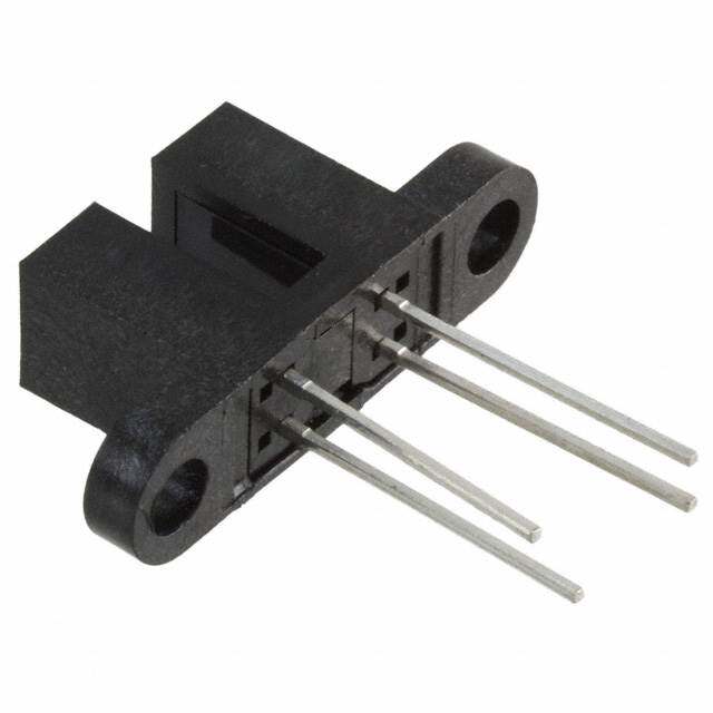
| 描述 | PROXIMITY SENSOR 25MM |
| 产品分类 | |
| 品牌 | Sharp Microelectronics |
| 数据手册 | http://www.sharpsma.com/download/GP2AP002S00Fpdf点击此处下载产品Datasheet |
| 产品图片 |
|
| 产品型号 | GP2AP002S00F |
| rohs | 无铅 / 符合限制有害物质指令(RoHS)规范要求 |
| 产品系列 | - |
| 传感器类型 | 红外线 |
| 其它名称 | 425-2785-1 |
| 响应频率 | - |
| 封装/外壳 | 8-SMD 模块 |
| 屏蔽 | - |
| 感应物体 | 非金属 |
| 感应距离 | 0.984"(25mm) |
| 材料-本体 | - |
| 标准包装 | 1 |
| 电压-电源 | 2.4 V ~ 3.6 V |
| 端子类型 | - |
| 输出类型 | 电流 |


- 商务部:美国ITC正式对集成电路等产品启动337调查
- 曝三星4nm工艺存在良率问题 高通将骁龙8 Gen1或转产台积电
- 太阳诱电将投资9.5亿元在常州建新厂生产MLCC 预计2023年完工
- 英特尔发布欧洲新工厂建设计划 深化IDM 2.0 战略
- 台积电先进制程称霸业界 有大客户加持明年业绩稳了
- 达到5530亿美元!SIA预计今年全球半导体销售额将创下新高
- 英特尔拟将自动驾驶子公司Mobileye上市 估值或超500亿美元
- 三星加码芯片和SET,合并消费电子和移动部门,撤换高东真等 CEO
- 三星电子宣布重大人事变动 还合并消费电子和移动部门
- 海关总署:前11个月进口集成电路产品价值2.52万亿元 增长14.8%

PDF Datasheet 数据手册内容提取
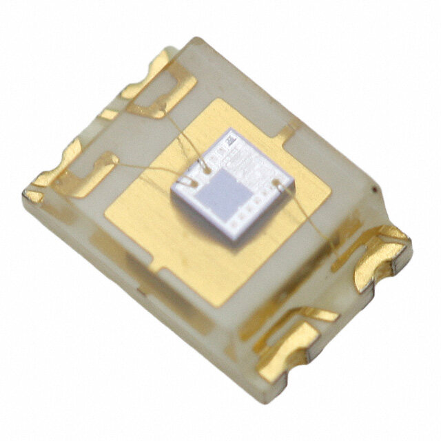
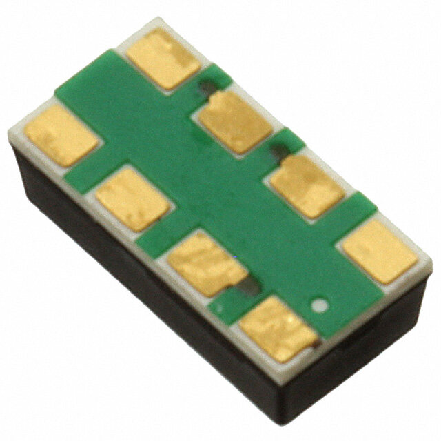
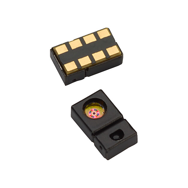
GP2AP002S00F GP2AP002S00F Proximity Sensor ■Description ■ Agency approvals/Compliance GP2AP002S00F provide a digital detection system 1. Compliant with RoHS directive (2002/95/EC) integrated into one package the light emitting element and a light receiving element. So small package size, it is easy to mount on the equipment. ■ Applications 1. Mobile phone 2. Smartphone, Tablet 3. Digital single-lens reflex camera ■Features 1. Disparities in detecting distance results are greatly reduced using a built-in circuit for reduction of light-detecting sensitivity disparities 2.Compact size(4.0 × 2.0 × 1.25t mm) 3.Built-in LED for simple optical design 4.I2C output type Notice The content of data sheet is subject to change without prior notice. In the absence of confirmation by device specification sheets, SHARP takes no responsibility for any defects that may occur in equipment using any SHARP devices shown in catalogs, data books, etc. Contact SHARP in order to obtain the latest device specification sheets before using any SHARP device. Sheet No.: OP13009EN 1
GP2AP002S00F ■ Schematic Internal Block Diagram Vcc Output buffer Synchronized ●● Vout AMP Signal Detection LEDA ●● Vio LED driver I2C SDA LEDC ●● Oscill ator Inte rface SCL Power on Reset GND Sheet No.: OP13009EN 2
GP2AP002S00F ■Outline Dimensions 1) area: Au plating 2) Unspecified tolerance shall be 0.2. 3) Adhesion of resin to the terminal area shall be allowed Max. 0.2mm. Sheet No.: OP13009EN 3
GP2AP002S00F ■Absolute Maximum Ratings Ta=25°C (unless otherwise specified) Parameter Symbol Rating Unit Remarks Supply voltage Vcc -0.3 to 3.8 V LED supply voltage V -0.3 to 3.8 V LED LED peak forward current I 300 mA LED -0.3 to Vcc+0.3 and Cf: Refer to the page 7, Directions for Logic I/O supply voltage Vio V 3.8V or less power-line connection Vio-0.3 to Vio+0.3 and Cf: Refer to the page 7, Directions for SDA/SCL pull-up voltage - V 3.8V or less power-line connection Operating temperature Topr -25 to +85 °C Storage temperature Tstg -40 to +85 °C Soldering temperature Tsol 260 °C peak temperature duration:10sec ■Recommended Operating Conditions Ta=25°C (unless otherwise specified) Parameter Symbol Operating condition Unit Remarks Supply voltage Vcc 2.4 to 3.6 V LED supply voltage V 2.4 to 3.6 V LED Operating temperature T -25 to 85 °C opr Logic I/O supply voltage Vio 1.65 to Vcc V SCL, SDA input low level VIL -0.3 to 0.2×Vio V SCL, SDA input high level VIH 0.8×Vio to Vio+0.3 V ■Electrical and Optical Characteristics Ta=25°C ,Vcc=3.3V, V =3.3V R =6.8Ω (unless otherwise specified) LED LED Parameter Symbol Min. Typ. Max. Unit Remarks No detection object, Ev=0 lx. operating mode I - 240 600 CC *1, except for LED and driver Current consumption uA No input signal. shutdown mode I - - 1.0 CC-S *1, except for LED and driver LED peak current I - 170 - mA LED Peak emission wavelength λ - 940 - nm p Vout terminal High level output voltage V Vio-0.5 Vio-0.3 Vio+0.3 V I =0.3mA,*2 OH OH Vout terminal Low level output voltage V - - 0.5 V I =1mA, *2 OL OL Response time (H→L) tp - - 50 ms *2 HL Response time (L→H) tp - - 50 ms LH Rise time tr - 1 - μs *2, CL=15pF Fall time tf - 1 - μs *3, Detection object: Maximum detection distance Lon 25 65 - mm KODAK Gray Card (r = 0.18) Operation mode B1 Minimum no detection distance Loff - 78 150 mm Wake up time tsdw - - 100 ms *4 Maximum acceptable illuminance Ev 3000 - - lx *5 SCL clock frequency SCL 4 - 400 kHz *1. Current consumption through VLED terminal (including LED and its driver output) depends on actual environment and situations. (See attached document【1】1-1) Sheet No.: OP13009EN 4
GP2AP002S00F *2. Parameters defined for Vout output waveform specifications With detection object State of the object to be detected Without detection object tp tp HL LH tf tr VOH 90% Vout output 50% (at normal output mode) 10% VOL *3. Detection distance KODAK Gray Card d GP2AP002S00F GP2AP002S00F output example vs. distance characteristics (operation mode B1) Mimimum No Detection Distance Maximum Detection Distance 1 n ue n→ ctio VO val detectio ←no dete 0 0 20 40 60 80 100 120 140 160 180 200 Distance, d (mm) Sheet No.: OP13009EN 5
GP2AP002S00F *4. Wake up time, tsdw, is defined as a delay of the 1st LED emission after issuing the I2C write command to release GP2AP002S00F from the shutdown mode. Note that there should be no external light noise sources in this particular examination. Also, by definition, it does not matter where reflective object is, but it is recommended that the object should be placed at d << Lon because VO is initialized to 0 and the next expected change is 0 to 1. *5. Test set-up for “Maximum Acceptable Illuminance” measurement GP2AP002S00F Light source A Emitter/Detector surface Illuminance should be measured and evaluated at Emitter/Detector surface of GP2AP002S00F. The maximum acceptable illuminance, Ev, is a maximum level of illuminance at which GP2AP002S00F should keep its sensing result, VO, as "0" (no detection) as long as no reflective objects exist. However, GP2AP002S00F may start to exhibit false detection with external light noise beyond this level. See attached document【1】1-10 for more details. ■Supplement ●This product is built-in photodiode. ●Compliance with each regulation 1) The RoHS directive(2002/95/EC) This product complies with the RoHS directive(2002/95/EC) . Object substances: mercury, lead, cadmium, hexavalent chromium, polybrominated biphenyls(PBB) and polybrominated diphenyl ethers(PBDE) 2) Content of six substances specified in Management Methods for Control of Pollution Caused by Electronic Information Electronic Information Products Regulation (Chinese : 电子信息产品污染控制管理办法). Toxic and hazardous substances Hexavalent Polybrominated Polybrominated Category Lead Mercury Cadmium chromium biphenyls diphenyl ethers (Pb) (Hg) (Cd) (Cr6+) (PBB) (PBDE) Proximity sensor ✓ ✓ ✓ ✓ ✓ ✓ ✓: indicates that the content of the toxic and hazardous substance in all the homogeneous materials of the part is below the concentration limit requirement as described in SJ/T 11363-2006 standard . ●This product shall not contain the following materials. Also, the following materials shall not be used in the production process for this product. Materials for ODS : CFCs, Halon, Carbon tetrachloride, 1,1,1-Trichloroethane (Methylchloroform) ●Brominated flame retardants Specific brominated flame retardants such as the PBB and PBDE are not used in this device at all. ●Product mass : Approx . 0.017 g ●Country of origin : China ●Packing : Refer to the attached sheet, Page 11. ●Moisture level: MSL3 Sheet No.: OP13009EN 6
GP2AP002S00F ■Notes ●Before the circuit design In circuit designing, make allowance for the degradation of the light emitting diode output that results from long continuous operation. (50% degradation/5 years) ●Please take proper methods to prevent ESD. The IC built in GP2AP002S00F is ESD-sensitive because it is fabricated by sub-micron CMOS process. For example, in handling GP2AP002S00F, human body and soldering iron etc. should be grounded. ●As it takes at most 100ms to let GP2AP002S00F go to active operation from shut-down mode, please take this delay into system design consideration. Also, if the host system relies on the actual value of this delay, e.g. to do frequent software shutdown, please thoroughly make sure that the operation be successful in any realistic situation. ●Regarding to prevention of malfunction To prevent GP2AP002S00F from faulty operation due to external light noise sources, do not set the detection surface to these sources directly. Under very unlikely situation, GP2AP002S00F output may fall into malfunction (See attached document 【1】1-10 for more detail). It can be reset by letting GP2AP002S00F go shutdown once, and then activating GP2AP002S00F again. In case of this, take it into consideration, in software implementation, to prepare a method to reset GP2AP002S00F. Also, if some other electronic components are placed close to this device, faulty operation may occur. (The light reflection caused by the other components may slip into the photo-detecting portion of the device and may cause faulty operation.) ●Directions for power-line connection Avoid that GP2AP002S00F’s SDA/SCL terminals are pulled-up to the other power line than GP2AP002S00F’s Vio terminal even if they are in the same operating voltage. See also 10) Recommended external circuit. For example, when you shut down GP2AP002S00F by letting Vcc and Vio terminals go to GND level (instead of using software shutdown function), and if GP2AP002S00F’s SDA/SCL terminals are still pulled-up to another active power line, these terminals will draw significant currents from a pull-up resister through internal ESD devices and the SCL and SDA lines are pulled-down, which causes system error (I2C bus error). Also, when you consider reducing total current consumption of the I2C devices by turning off the power line(s), avoid that one of the Vcc and Vio terminals of GP2AP002S00F is turned off and the other is kept on. It never shuts down GP2AP002S00F’s current consumption, but possibly yields excessive current between these power lines. Please consider making use of “software shutdown” function. However, when you do have to turn off one of these power lines (Vcc, Vio, SDA/SCL pull-up level), all of them in GP2AP002S00F should be turned off for the purpose of choking GP2AP002S00F’s current consumption regardless of the register setting for the software shutdown function. ●Directions for I2C-bus interface GP2AP002S00F is equipped with a 7-bit address as a slave device on the I2C bus interface. Through the SDA and SCL terminals, GP2AP002S00F’s registers can be set up, and also GP2AP002S00F’s sensing result can be read out. However, the read format specified for GP2AP002S00F is a proprietary one that differs from the normal read format (immediately after the first byte) or the combined format shown in the I2C-bus specification version 2.1, January 2000. For more details to let GP2AP002S00F operate properly, see attached document【1】1-2, I2C-bus interface, and 【2】 recommended operation mode / register setting procedure. ●After being mounted and soldered, if GP2AP002S00F is deformed by external force or impact, e.g. something falls onto the device, it may result in defective implementation such as lift-off of the terminals. Careful handling should be taken. ●For soldering Refer to the page 10 ●For cleaning Cleaning shall carry out as the below items to avoid keeping solvent, solder and flux on the device (1) Solvent cleaning : Solvent temperature 45°C or less, Immersion for 3 min or less (2) Ultrasonic cleaning : Please don't carry out ultrasonic cleaning. (3) The cleaning shall be carried out with solvent below. Solvent : Ethyl alcohol, Methyl alcohol, Isopropyl alcohol Sheet No.: OP13009EN 7
GP2AP002S00F ●Recommended external circuit (Top View) Components Recommended values CX1 4.7uF (Ceramic) CX2 0.1uF (Ceramic) CX3 1.0uF (Ceramic) CX4 10uF (Ceramic) R1 1/20W 10 Ω R 1/20W 6.8Ω±1% (V =V =3.3V) LED CC LED Rp 1/20W 10k Ω (*) Notes: Place the capacitors CX1~CX4 as close as possible to the corresponding terminals. For CX1~CX3, at most 5mm or less is preferable. Depending on the level and/or frequency component(s) of the power supply noise, CX’s and R1 listed above may not completely eliminate its influence. Therefore, to avoid GP2AP002S00F's false detection which can be greatly influenced by the supply noises, please carefully make sure that there is no problem with the actual electrical implementation. Whenever considering to change V voltage, choose proper value for R so that the desired I is obtained. LED LED LED SDA terminal (as output) and LEDA terminal are NMOS open-drain output. On the other hand, Vout terminal is CMOS output, but it has no high-impedance state. (*) To determine the appropriate value for Rp’s, see section 16 of The I2C-Bus Specification. Sheet No.: OP13009EN 8
GP2AP002S00F ●Foot pattern of PCB Dimensions are shown for reference. Top View Mount center 1. Dimension in parenthesis are shown for reference. 2. Unit : mm Pin Pin name Symbol ① LED Anode LEDA ② LED Cathode LEDC ③ Vcc Vcc ④ Output Vout ⑤ Ground GND ⑥ Logic I/O Supply Voltage Vio ⑦ I2C DATA BUS SDA ⑧ I2C CLOCK SCL ●Recommendable size of solder creamed paste (Reference) : Soldering paste area * Dimension in parenthesis are shown for reference. Unit : mm Sheet No.: OP13009EN 9
GP2AP002S00F ■Precautions for Soldering 1. In case of solder reflow Reflow is allowed only twice at the temperature and the time within the temperature profile as shown in the figure below. Reflow interval shall be within 7days under conditions, 10 to 30°C, 70%RH or less. MAX 260°C 1~5°C/s 220°C 190°C 1~5°C/s 150°C 1~5°C/s 25°C MAX10s MAX50s MAX120s 2. Other precautions An infrared lamp used to heat up for soldering may cause a localized temperature rise in the resin. Also avoid immersing the resin part in the soldering. Even if within the temperature profile above, there is the possibility that the gold wire in package is broken in case that the deformation of PCB gives the affection to lead pins. Please use after confirmation the conditions fully actual solder reflow machine. Sheet No.: OP13009EN 10
GP2AP002S00F ■Packing P acking Inner Packing ① Inner Packaging drawing Caver tape 2,000pcs products Carrier tape ②Inner packing material:・Reel(PPE) ・Carrier tape (PC) ・Caver tape(PET) ③Quantity :2,000pcs./Reel Taping reel containing products Outer Packaging EIAJ C-3Label ① Outer Packaging drawing Silica gel Humidity indicator EIAJ C-3Label Aluminium laminated sack Aluminium laminated sack containing a taping reel Cushioning material Aluminium laminated bag with tape-reel (5 bags) Packing case Kraft tape EIAJ C-3Label ②Outer packing material: Packing case(Corrugated cardboard), Cushioning material (Urethane) Aluminium laminated bag (Alumi-Polyethylene) Humidity indicator card (paper), Label(paper), silica gel, craft tape ③Quantity: 10,000pcs./box ④The contents of the carton indication conforms to EIAJ C-3 and the following items are indicated. Model No., Internal production control name, Quantity, Packing date, Corporate name, Country of origin ⑤Regular packaged mass: Approximately 700g Sheet No.: OP13009EN 11
GP2AP002S00F ■Important Notices · The circuit application examples in this publication are with equipment that requires higher reliability such as: provided to explain representative applications of SHARP --- Transportation control and safety equipment (i.e., devices and are not intended to guarantee any circuit aircraft, trains, automobiles, etc.) design or license any intellectual property rights. SHARP --- Traffic signals takes no responsibility for any problems related to any --- Gas leakage sensor breakers intellectual property right of a third party resulting from --- Alarm equipment the use of SHARP's devices. --- Various safety devices, etc. (iii) SHARP devices shall not be used for or in connection · Contact SHARP in order to obtain the latest device with equipment that requires an extremely high level of specification sheets before using any SHARP device. reliability and safety such as: SHARP reserves the right to make changes in the --- Space applications specifications, characteristics, data, materials, structure, --- Telecommunication equipment [trunk lines] and other contents described herein at any time without --- Nuclear power control equipment notice in order to improve design or reliability. --- Medical and other life support equipment (e.g., Manufacturing locations are also subject to change without scuba). notice. · If the SHARP devices listed in this publication fall within · Observe the following points when using any devices in the scope of strategic products described in the Foreign this publication. SHARP takes no responsibility for Exchange and Foreign Trade Law of Japan, it is necessary damage caused by improper use of the devices which does to obtain approval to export such SHARP devices. not meet the conditions and absolute maximum ratings to be used specified in the relevant specification sheet nor · This publication is the proprietary product of SHARP and meet the following conditions: is copyrighted, with all rights reserved. Under the (i) The devices in this publication are designed for use in copyright laws, no part of this publication may be general electronic equipment designs such as: reproduced or transmitted in any form or by any means, --- Personal computers electronic or mechanical, for any purpose, in whole or in --- Office automation equipment part, without the express written permission of SHARP. --- Telecommunication equipment [terminal] Express written permission is also required before any use --- Test and measurement equipment of this publication may be made by a third party. --- Industrial control --- Audio visual equipment · Contact and consult with a SHARP representative if there --- Consumer electronics are any questions about the contents of this publication. (ii) Measures such as fail-safe function and redundant design should be taken to ensure reliability and safety when SHARP devices are used for or in connection Sheet No.: OP13009EN 12