ICGOO在线商城 > GP1UD282XK
 Datasheet下载
- 型号: GP1UD282XK
- 制造商: Sharp Microelectronics
- 库位|库存: xxxx|xxxx
- 要求:
| 数量阶梯 | 香港交货 | 国内含税 |
| +xxxx | $xxxx | ¥xxxx |
查看当月历史价格
查看今年历史价格
GP1UD282XK产品简介:
ICGOO电子元器件商城为您提供GP1UD282XK由Sharp Microelectronics设计生产,在icgoo商城现货销售,并且可以通过原厂、代理商等渠道进行代购。 提供GP1UD282XK价格参考以及Sharp MicroelectronicsGP1UD282XK封装/规格参数等产品信息。 你可以下载GP1UD282XK参考资料、Datasheet数据手册功能说明书, 资料中有GP1UD282XK详细功能的应用电路图电压和使用方法及教程。
| 参数 | 数值 |
| B.P.F.中心频率 | 36.7kHz |
| 产品目录 | |
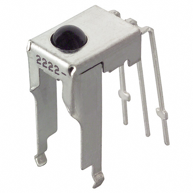
| 描述 | RECEIVER REMOTE CTRL TOP 36.7KHZ |
| 产品分类 | |
| 品牌 | Sharp Microelectronics |
| 数据手册 | |
| 产品图片 |
|
| 产品型号 | GP1UD282XK |
| rohs | 含铅 / 不符合限制有害物质指令(RoHS)规范要求 |
| 产品系列 | * |
| 产品目录绘图 |
|
| 产品目录页面 | |
| 其它名称 | 425-1126 |
| 安装类型 | 通孔 |
| 感应距离 | 10m |
| 朝向 | 顶视图 |
| 标准包装 | 200 |
| 电压-电源 | 2.7 V ~ 5.5 V |
| 电流-电源 | 200µA |


- 商务部:美国ITC正式对集成电路等产品启动337调查
- 曝三星4nm工艺存在良率问题 高通将骁龙8 Gen1或转产台积电
- 太阳诱电将投资9.5亿元在常州建新厂生产MLCC 预计2023年完工
- 英特尔发布欧洲新工厂建设计划 深化IDM 2.0 战略
- 台积电先进制程称霸业界 有大客户加持明年业绩稳了
- 达到5530亿美元!SIA预计今年全球半导体销售额将创下新高
- 英特尔拟将自动驾驶子公司Mobileye上市 估值或超500亿美元
- 三星加码芯片和SET,合并消费电子和移动部门,撤换高东真等 CEO
- 三星电子宣布重大人事变动 还合并消费电子和移动部门
- 海关总署:前11个月进口集成电路产品价值2.52万亿元 增长14.8%

PDF Datasheet 数据手册内容提取
GP1UD26XK Series/GP1UD27XK Series/GP1UD28XK Series/GP1UD28YK Series GP1UD26XK Series/GP1UD27XK Series Energy Saving Type Low Dissipation GP1UD28XK Series/GP1UD28YK Series Current IR Detecting Unit for Remote Control (cid:2) Features (cid:2) Applications 1.Low dissipation current:MAX.200µA (at V =3V) 1.Audio video equipment CC (1/12 of conventional type) 2.Home appliances 2.Wide operating voltage range (2.7 to 5.5V) 3.Various attachment shape (cid:2) Outline Dimensions (Unit : mm) GP1UD26XK 0S.5e7r.3ies 1.6 5.2 3.6+0.51.1−0.31.4 GP1UD27XK S0.e75r.i3es 1.6 10.4 3.6+0.51.1−0.31.4 3.4 2.8 3.4 2.8 2 2 10. *1 13.1 D26 Mar4king 1.4 10. *1 13.1 D27 Ma4rking 1.4 0. 0. *1 2.54 2.54 *1 4 *1 2.54 2.54 *1 4 R1.9 R1.9 Recommended drilling as viewed from the soldering face. Recommended drilling as viewed from the soldering face. 2-0.5 1.7 3.753.751.21.7 12 VVOCCUT 1.7 3.753.751.21.7 2-0.750.6 1 2 3 20-0.6.4 Dceentetecrt or 10.45 1.2 (0.5) (9.7)8.75 2-02.-705.5 2-30.4GNDDceentetecrtor 10.45 1.2 (0.5) (9.7)8.75 123 VVGOCNCUDT 2.54 2.54φ0.8 0.6 1 2 3 0.6 2.54 2.54φ0.8 ❈ Unspecified tolerance:±0.3 ❈ *1:The dimension of lead base ❈ Unspecified tolerance:±0.3 ❈ *1:The dimension of lead base GP1UD28XK Series GP1UD28YK Series 0.75.3 1.6 14.4 3.6+0.51.1−0.31.4 0.57.3 1.6 4 10.2 3.413.1 D28 Marking 1.4 2.8 3.413 D28 Marking *1 4 0. 0.4 *1 2.54 2.54 *1R1.9 4 3.6 1.6 1.4 Recommended drilling as viewed from the soldering face. 0.6 1 2 3 0.6 3.7 1.4 3.753.75 5.4 123 VVGOCNCUDT 1.745 1.2 1.21.7 123 VVGOCNCUDT R1.9 Recommended2 d.r5illi4ng as vie6w.e8d2 fφr.o50m.4 8th95e soldering face. 2-0.5 Dceentetecrtor 10. (0.5)(9.7)8.75 3.65 1. 2-0.4 7 2-0.75 0.5 7 1.2 1.2 1. 0.6 1 2 3 0.6 2.54 2.54φ0.8 *1 2.54 *1 2.54 1. 3.753.75 ❈ Unspecified tolerance:±0.3 ❈ *1:The dimension of lead base ❈ Unspecified tolerance:±0.3 ❈ *1:The dimension of lead base Notice In the absence of confirmation by device specification sheets, SHARP takes no responsibility for any defects that may occur in equipment using any SHARP devices shown in catalogs, data books, etc. Contact SHARP in order to obtain the latest device specification sheets before using any SHARP device. Internet Internet address for Electronic Components Group http://www.sharp.co.jp/ecg/
GP1UD26XK Series/GP1UD27XK Series/GP1UD28XK Series/GP1UD28YK Series (cid:2) Absolute Maximum Ratings (Ta=25°C) Parameter Symbol Rating Unit Supply voltage VCC 0 to +6.0 V *1Operating temperature Topr −10 to +70 °C Storage temperature Tstg −20 to +70 °C *2Soldering temperature Tsol 260 (5s) °C *1 No dew condensation is allowed *2 At mounting on PCB with thickness of 1.6mm (cid:2) Recommended Operating Conditions Parameter Symbol Operating conditions Unit Supply voltage VCC 2.7 to 5.5 V (cid:2) Electro-optical Characteristics (Unless otherwise specified, condition shall be Ta=25˚C, VCC=3V) Parameter Symbol Conditions MIN. TYP. MAX. Unit Dissipation current ICC No input light − − 200 µA High level output voltage VOH *3 VCC −0.5 − − V Low level output voltage VOL *3 IOL=100µA − − 0.5 V High level pulse width T1 *3 700 − 1 200 µs Low level pulse width T2 *3 400 − 900 µs B.P.F. center frequency fO − − *4 − kHz *3The burst wave as shown in the following figure shall be transmitted by the transmitter shown in Fig.2 The carrier frequency of the transmitter, however, shall be same as *4. Measuring shall be from just after starting the transmission until 50 pulse *4The B.P.F. center frequency fo varies with model, as shown in (cid:2) Model Line-ups Burst Wave fO=*4 kHz Duty 50% Transmitter signal 600µs 1 000µs Output signal T2 T1 (cid:2) Model Line-up B.P.F. center Model No. 40kHz GP1UD26XK GP1UD27XK GP1UD28XK GP1UD28YK 36kHz GP1UD260XK GP1UD270XK GP1UD280XK GP1UD280YK 38kHz GP1UD261XK GP1UD271XK GP1UD281XK GP1UD281YK 36.7kHz GP1UD262XK GP1UD272XK GP1UD282XK GP1UD282YK 32.75kHz GP1UD263XK GP1UD273XK GP1UD283XK GP1UD283YK 56.8kHz GP1UD267XK GP1UD277XK GP1UD287XK GP1UD287YK
GP1UD26XK Series/GP1UD27XK Series/GP1UD28XK Series/GP1UD28YK Series Fig.1 Internal Block Diagram TYP. 100kΩ AMP Limiter B.P.F. Demodulator Integrator Comparator GND VCC VOUT (cid:2) Performance Using the transmitter shown in Fig.2, the output signal of the light detecting unit is good enough to meet the following items in the standard optical system in Fig.3. 1. Linear reception distance characteristics When L=0.2 to 10.0m, *5 E <10 lx and φ=0˚ in Fig.3, the output signal shall meet the electrical characteristics in the attached list. V 2.Sensitivity angle reception distance characteristics When L=0.2 to 7.5m, *5 E <10 lx and φ≤30˚ in Fig.3, the output signal shall meet the electrical characteristics in the attached list. V 3.Anti outer peripheral light reception distance characteristics When L=0.2 to 5.0m, *5,*6 E ≤ 300 lx and φ=0˚ in Fig.3, the output signal shall meet the electrical characteristics in the attached list. V *5 It refers to detector face illuminance *6 Outer peripheral light source: CIE standard light source A shall be used and placed at 45˚ from perpendicular axis at the detector face center Fig.2 Transmitter 20cm 10kΩ +5V PI 9 F D4 µ0 P 1 Transmitter (GL521 used) fO=*4 Duty 50% Ω 0k VOUT 1 Oscilloscope In the above figure, the transmitter should be set so that the output V (peak-to-peak) can be 40m V OUT However, the PD49PI to be used here should be of the short-circuit current I =2.6µA at E =100 lx SC V (E is an illuminance by CIE standard light source A (tungsten lamp).) V
GP1UD26XK Series/GP1UD27XK Series/GP1UD28XK Series/GP1UD28YK Series Fig.3 Standard Optical System Light detector face illuminance:EV φ φ VOUT Reception distance:L Transmitter (φ indicates horizontal and vertical directions.) Fig.4 B.P.F.Frequency Characteristics Fig.5 Sensitivity Angle (Horizontal Direction) (TYP.) Characteristics (TYP.) (Reference) −15˚ 0˚ +15˚ −30˚ 100 %) +30˚ B/div) distance ( 80 Relative sensitivity (5d −−4650˚˚ Relative reception 6400 ++4650˚˚ 20 −75˚ +75˚ VCC=5V Ta=25˚C −90˚ +90˚ 10 20 30 40 50 60 Carrier frequency (kHz) Fig.6 Sensitivity Angle (Vertical Direction) Fig.7 Relative Reception Distance vs.Ambient Characteristics (TYP.) (Reference) Temperature (TYP.) (Reference) −15˚ 0˚ +15˚ 120 −30˚ 100 +30˚ VCC=5V %) %) 100 distance ( 80 distance ( 80 VCC=3V n n −−6405˚˚ Relative receptio 6400 ++6405˚˚ ve communicatio 4600 Unit NstaEnCd ard transmitter −75˚ 20 +75˚ Relati 20 Rdiesltaatnivcee caot m φp=a0r˚i,s oEnV <w1it0hl xre ception VCC=5V and Ta=25˚C taken as 100% Ta=25˚C 0 −90˚ +90˚ −20 −10 0 10 20 30 40 50 60 70 80 Ambient Temperature (˚C)
GP1UD26XK Series/GP1UD27XK Series/GP1UD28XK Series/GP1UD28YK Series Fig.8 AEHA (Japan Association of Electrical Home Appliances) Code Fig.9 AEHA (Japan Association of Electrical Home Appliances) Code Pulse Width Characteristics (1st Bit) (TYP.) (Reference) (V =3V) Pulse Width Characteristics (1st, Bit) (TYP.) (Reference) (V =5V) CC CC 600 600 Low level pulse width Low level pulse width 500 500 400 400 µs) µs) h ( h ( ulse widt 300 High level pulse width ulse widt 300 High level pulse width P 200 P 200 Unit AEHA code Unit AEHA code 100 generating transmitter 1st bit 100 generating transmitter 1st bit VCC=3V, Ta=RT, φ=0˚, VCC=5V, Ta=RT, φ=0˚, 0 EV<10lx, T=420µs 0 EV<10 lx, T=420µs 0 2 4 6 8 10 12 14 0 2 4 6 8 10 12 14 Receiving distance (m) Receiving distance (m) Fig.10 Dissipation Current vs. Supply Fig.11 Spectral Sensitivity (Reference) Voltage 200 100 180 90 160 80 A) µDissipation current I (CC 1116802400000 Ta=RT Relative sensitivity (%) 3456700000 40 φ=0˚ 20 20 EV<10 lx 10 No input light 0 2 2.5 3 3.5 4 4.5 5 5.5 6 700 800 900 1 000 1 100 1 200 Supply voltage VCC (V) Wavelength λ (nm)
GP1UD26XK Series/GP1UD27XK Series/GP1UD28XK Series/GP1UD28YK Series (cid:2) Precautions for Operation 1. When this infrared remote control detecting unit shall be adopted for wireless remote control, please use it with the signal format of transmitter, which total duty ratio D (Emitting time Σn t / Transmitting time for 1 block T) is 40% or less. ON signal time T t N=1N ON (Pulse width of the presence of modulated IR) should be 250µs or more. In case that the signal format of total duty and ON signal time is out of above conditions, there is a case that reception distance is much reduced or output is not appeared. Transmitting time for 1 block:T TON t1 t2 t3 tn n Dt=( Σ tN / T)×100 (%) N=1 2. Use the light emitting unit (remote control transmitter), in consideration of performance, characteristics, operating conditions of light emitting device and the characteristics of the light detecting unit. 3. Pay attention to a malfunction of the light detecting unit when the surface is stained with dust and refuse. Care must be taken not to touch the light detector surface. If it should be dirty, wipe off such dust and refuse with soft cloth so as to prevent scratch. In case some solvents are required, use methyl alcohol, ethyl alcohol or isopropyl alcohol only. Also, protect the light detecting unit against flux and others, since their deposition on the unit inside causes reduction of the function, fading of markings such as the part number. 4. The shield case should be grounded on PCB pattern. (The area across the shield case and the GND terminal is internally conductive in some cases and non-conductive in some other cases.) 5. Do not apply unnecessary force to the terminal and the case. 6. Do not push the light detector surface (photodiode) from outside. 7. To avoid the electrostatic breakdown of IC, handle the unit under the condition of grounding with human body, soldering iron, etc. 8. Do not use hole and groove set in the case of the light detecting unit for other purposes, since they are required to maintain the specified performance. 9. External Circuit Examples (Mount the outer parts as near the unit as possible). GND GND CO+ R1 VCC Ve (Circuit parameters) VOUT VO R1=47Ω±5% C1=47µF In setting R and C, use suitable values after considering under the real condition 1 1 10. There is a possibility that noise on output may be caused by environmental condition (Disturbing light noise, Electromagnetic noise, Power supply line noise, etc.) even if there is no input transmission signal. 11. Please shall confirm operation or your actual machine. Because the output pulse width of this product is fluctuated by environmental conditions such as signal format, temperature, distance from transmitter, and so on.
Application Circuits NOTICE lThe circuit application examples in this publication are provided to explain representative applications of SHARP devices and are not intended to guarantee any circuit design or license any intellectual property rights. SHARP takes no responsibility for any problems related to any intellectual property right of a third party resulting from the use of SHARP's devices. lContact SHARP in order to obtain the latest device specification sheets before using any SHARP device. SHARP reserves the right to make changes in the specifications, characteristics, data, materials, structure, and other contents described herein at any time without notice in order to improve design or reliability. Manufacturing locations are also subject to change without notice. lObserve the following points when using any devices in this publication. SHARP takes no responsibility for damage caused by improper use of the devices which does not meet the conditions and absolute maximum ratings to be used specified in the relevant specification sheet nor meet the following conditions: (i) The devices in this publication are designed for use in general electronic equipment designs such as: --- Personal computers --- Office automation equipment --- Telecommunication equipment [terminal] --- Test and measurement equipment --- Industrial control --- Audio visual equipment --- Consumer electronics (ii)Measures such as fail-safe function and redundant design should be taken to ensure reliability and safety when SHARP devices are used for or in connection with equipment that requires higher reliability such as: --- Transportation control and safety equipment (i.e., aircraft, trains, automobiles, etc.) --- Traffic signals --- Gas leakage sensor breakers --- Alarm equipment --- Various safety devices, etc. (iii)SHARP devices shall not be used for or in connection with equipment that requires an extremely high level of reliability and safety such as: --- Space applications --- Telecommunication equipment [trunk lines] --- Nuclear power control equipment --- Medical and other life support equipment (e.g., scuba). lContact a SHARP representative in advance when intending to use SHARP devices for any "specific" applications other than those recommended by SHARP or when it is unclear which category mentioned above controls the intended use. lIf the SHARP devices listed in this publication fall within the scope of strategic products described in the Foreign Exchange and Foreign Trade Control Law of Japan, it is necessary to obtain approval to export such SHARP devices. lThis publication is the proprietary product of SHARP and is copyrighted, with all rights reserved. Under the copyright laws, no part of this publication may be reproduced or transmitted in any form or by any means, electronic or mechanical, for any purpose, in whole or in part, without the express written permission of SHARP. Express written permission is also required before any use of this publication may be made by a third party. lContact and consult with a SHARP representative if there are any questions about the contents of this publication. 115