ICGOO在线商城 > 集成电路(IC) > 逻辑器件 - 转换器,电平移位器 > FXMA108BQX

 Datasheet下载
- 型号: FXMA108BQX
- 制造商: Fairchild Semiconductor
- 库位|库存: xxxx|xxxx
- 要求:
| 数量阶梯 | 香港交货 | 国内含税 |
| +xxxx | $xxxx | ¥xxxx |
查看当月历史价格
查看今年历史价格
FXMA108BQX产品简介:
ICGOO电子元器件商城为您提供FXMA108BQX由Fairchild Semiconductor设计生产,在icgoo商城现货销售,并且可以通过原厂、代理商等渠道进行代购。 FXMA108BQX价格参考。Fairchild SemiconductorFXMA108BQX封装/规格:逻辑器件 - 转换器,电平移位器, 双向 电压电平 转换器 1 电路 8 通道 100Mbps 20-DQFN(2.5x4.5)。您可以下载FXMA108BQX参考资料、Datasheet数据手册功能说明书,资料中有FXMA108BQX 详细功能的应用电路图电压和使用方法及教程。
| 参数 | 数值 |
| 产品目录 | 集成电路 (IC)半导体 |
| 描述 | TRANSLATOR 8BIT DUAL 3ST 20DQFN转换 - 电压电平 Dual Supply 8-Bit Voltage Translator |
| 产品分类 | 逻辑 - 变换器集成电路 - IC |
| 品牌 | Fairchild Semiconductor |
| 产品手册 | |
| 产品图片 |
|
| rohs | 符合RoHS无铅 / 符合限制有害物质指令(RoHS)规范要求 |
| 产品系列 | 逻辑集成电路,转换 - 电压电平,Fairchild Semiconductor FXMA108BQX- |
| 数据手册 | |
| 产品型号 | FXMA108BQX |
| 产品种类 | 转换 - 电压电平 |
| 传播延迟(最大值) | 5.5ns |
| 位数 | 8 |
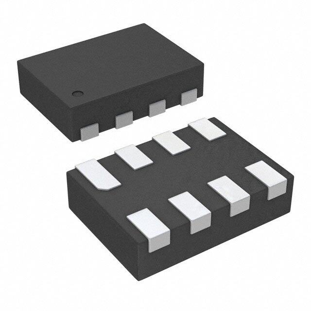
| 供应商器件封装 | 20-DQFN |
| 其它名称 | FXMA108BQXDKR |
| 包装 | Digi-Reel® |
| 单位重量 | 123 mg |
| 商标 | Fairchild Semiconductor |
| 安装类型 | 表面贴装 |
| 安装风格 | SMD/SMT |
| 封装 | Reel |
| 封装/外壳 | 20-WQFN 裸露焊盘,20-DQFN |
| 封装/箱体 | QFN-20 |
| 工作温度 | -40°C ~ 85°C |
| 工厂包装数量 | 3000 |
| 差分-输入:输出 | 无/无 |
| 数据速率 | 80Mbps |
| 最大工作温度 | + 85 C |
| 最小工作温度 | - 40 C |
| 标准包装 | 1 |
| 电压-电源 | 1.65 V ~ 5.5 V |
| 电源电压-最大 | 5.5 V |
| 电源电压-最小 | 1.65 V |
| 系列 | FXMA108 |
| 输入类型 | 逻辑 |
| 输出/通道数 | 1 |
| 输出类型 | 逻辑 |
| 通道数 | 8 |
| 逻辑功能 | 变换器,双向,单向,3 态 |


- 商务部:美国ITC正式对集成电路等产品启动337调查
- 曝三星4nm工艺存在良率问题 高通将骁龙8 Gen1或转产台积电
- 太阳诱电将投资9.5亿元在常州建新厂生产MLCC 预计2023年完工
- 英特尔发布欧洲新工厂建设计划 深化IDM 2.0 战略
- 台积电先进制程称霸业界 有大客户加持明年业绩稳了
- 达到5530亿美元!SIA预计今年全球半导体销售额将创下新高
- 英特尔拟将自动驾驶子公司Mobileye上市 估值或超500亿美元
- 三星加码芯片和SET,合并消费电子和移动部门,撤换高东真等 CEO
- 三星电子宣布重大人事变动 还合并消费电子和移动部门
- 海关总署:前11个月进口集成电路产品价值2.52万亿元 增长14.8%


PDF Datasheet 数据手册内容提取
Is Now Part of To learn more about ON Semiconductor, please visit our website at www.onsemi.com Please note: As part of the Fairchild Semiconductor integration, some of the Fairchild orderable part numbers will need to change in order to meet ON Semiconductor’s system requirements. Since the ON Semiconductor product management systems do not have the ability to manage part nomenclature that utilizes an underscore (_), the underscore (_) in the Fairchild part numbers will be changed to a dash (-). This document may contain device numbers with an underscore (_). Please check the ON Semiconductor website to verify the updated device numbers. The most current and up-to-date ordering information can be found at www.onsemi.com. Please email any questions regarding the system integration to Fairchild_questions@onsemi.com. ON Semiconductor and the ON Semiconductor logo are trademarks of Semiconductor Components Industries, LLC dba ON Semiconductor or its subsidiaries in the United States and/or other countries. ON Semiconductor owns the rights to a number of patents, trademarks, copyrights, trade secrets, and other intellectual property. A listing of ON Semiconductor’s product/patent coverage may be accessed at www.onsemi.com/site/pdf/Patent-Marking.pdf. ON Semiconductor reserves the right to make changes without further notice to any products herein. ON Semiconductor makes no warranty, representation or guarantee regarding the suitability of its products for any particular purpose, nor does ON Semiconductor assume any liability arising out of the application or use of any product or circuit, and specifically disclaims any and all liability, including without limitation special, consequential or incidental damages. Buyer is responsible for its products and applications using ON Semiconductor products, including compliance with all laws, regulations and safety requirements or standards, regardless of any support or applications information provided by ON Semiconductor. “Typical” parameters which may be provided in ON Semiconductor data sheets and/or specifications can and do vary in different applications and actual performance may vary over time. All operating parameters, including “Typicals” must be validated for each customer application by customer’s technical experts. ON Semiconductor does not convey any license under its patent rights nor the rights of others. ON Semiconductor products are not designed, intended, or authorized for use as a critical component in life support systems or any FDA Class 3 medical devices or medical devices with a same or similar classification in a foreign jurisdiction or any devices intended for implantation in the human body. Should Buyer purchase or use ON Semiconductor products for any such unintended or unauthorized application, Buyer shall indemnify and hold ON Semiconductor and its officers, employees, subsidiaries, affiliates, and distributors harmless against all claims, costs, damages, and expenses, and reasonable attorney fees arising out of, directly or indirectly, any claim of personal injury or death associated with such unintended or unauthorized use, even if such claim alleges that ON Semiconductor was negligent regarding the design or manufacture of the part. ON Semiconductor is an Equal Opportunity/Affirmative Action Employer. This literature is subject to all applicable copyright laws and is not for resale in any manner.
F X M A 1 July 2010 0 8 — D u FXMA108 a l - S Dual-Supply, 8-Bit Signal Translator with Configurable u p p Voltage Supplies and Signals Levels, 3-State Outputs l y , and Auto Direction Sensing 8 - B i t S i g n a Features Description l T r (cid:131) Bi-Directional Interface between Two Levels from The FXMA108 is a configurable dual-voltage supply a 1.65V to 5.5V translator designed for both uni-directional and bi- ns directional voltage translation between two logic levels. l (cid:131) Fully Configurable: Inputs and Outputs Track VCC The device allows translation between voltages as high at o (cid:131) Non-Preferential Power-Up; Either VCC may be as 5.5V to as low as 1.65V. The A port tracks the VCCA r Powered-Up First level and the B port tracks the VCCB level. This allows for w bi-directional voltage translation over a variety of it (cid:131) Outputs Remain in 3-State Until Active VCC Level is voltage levels: 1.8V, 2.5V, 3.3V, and 5.0V. h Reached C The device remains in 3-state until both V s reach o (cid:131) Outputs Switch to 3-State if Either VCC is at GND active levels, allowing either VCC to be powereCdC-up first. nf (cid:131) Power-Off Protection Internal power-down control circuits place the device in ig 3-state if either V is removed. u (cid:131) Bus Hold On Data Inputs Eliminates the Need for CC ra Pull-Up Resistors The /OE input, when high, disables both the A and B b Side by placing them in a 3-state condition. The /OE le (cid:131) Control Input (/OE) is Referenced to VCCA Voltage input is supplied by VCCA. V (cid:131) Packaged in 20-Terminal DQFN The FXMA108 supports bi-directional translation without ol t (cid:131) Direction Control Not Needed the need for a direction control pin. The two sides of the ag device have auto-direction-sense capability. Either port e (cid:131) 80Mbps Throughput when Translating between may sense an input signal and transfer it as an output S 2.5V and 5.0V signal to the other port. u p (cid:131) ESD Protection Exceeds: p l i − 8kV Human Body Model (B Port I/O to GND) Applications e s (JESD22-A114 & Mil Std 883e 3015.7) a − 5kV Human Body Model (A Port I/O to GND) (cid:131) Cell Phones, PDA, Digital Camera, Portable GPS, n (JESD22-A114 & Mil Std 883e 3015.7) and Storage d S − 2kV Charged Device Model (ESD STM 5.3) i g (JESD22-C101) n a l L e v Ordering Information e l s Operating Packing Part Number Package Temperature Range Method FXMA108BQX -40 to 85°C 20-Lead, DQFN, JEDEC MO-241, 2.5x4.5mm 3000 Units Tape and Reel © 2010 Fairchild Semiconductor Corporation www.fairchildsemi.com FXMA108 • Rev. 1.0.1
F X M A Functional Diagram 1 0 8 — D u a l - S u p p l y , 8 - B i t S i g n a l T r a n s l a t o r w i t h C o n f i g u r a Figure 1. Block Diagram b l e V o l t a g Functional Table e S u Control p Outputs p /OE li e s LOW Logic Level Normal Operation a HIGH Logic Level 3-State n d S ig n a l L e v e l s © 2010 Fairchild Semiconductor Corporation www.fairchildsemi.com FXMA108 • Rev. 1.0.1 2
F X Pin Configuration M A 1 VCCA VCCB 0 8 1 20 — D A0 2 19 B0 u a A1 3 18 B1 l-S u A2 4 17 B2 pp l y A3 5 16 B3 , 8 - A4 6 15 B4 B i t S A5 7 14 B5 i g n A6 8 13 B6 a l T A7 9 12 B7 ra n s 10 11 l a t GND /OE o r w Figure 2. Pin Configuration (Top Through View) i t h C Pin Definitions o n f Pin # Name Description ig u 1 VCCA A-Side Power Supply ra b 2 A0 A-Side Inputs or 3-State Outputs l e 3 A1 A-Side Inputs or 3-State Outputs V o 4 A2 A-Side Inputs or 3-State Outputs l t a 5 A3 A-Side Inputs or 3-State Outputs g e 6 A4 A-Side Inputs or 3-State Outputs S u 7 A5 A-Side Inputs or 3-State Outputs p p 8 A6 A-Side Inputs or 3-State Outputs l i e 9 A7 A-Side Inputs or 3-State Outputs s 10 GND Ground a n 11 /OE Output Enable Input d S 12 B7 B-Side Inputs or 3-State Outputs i g 13 B6 B-Side Inputs or 3-State Outputs n a l 14 B5 B-Side Inputs or 3-State Outputs L e 15 B4 B-Side Inputs or 3-State Outputs v e 16 B3 B-Side Inputs or 3-State Outputs l s 17 B2 B-Side Inputs or 3-State Outputs 18 B1 B-Side Inputs or 3-State Outputs 19 B0 B-Side Inputs or 3-State Outputs 20 V B-Side Power Supply CCB DAP NC No Connect © 2010 Fairchild Semiconductor Corporation www.fairchildsemi.com FXMA108 • Rev. 1.0.1 3
F X Absolute Maximum Ratings M A Stresses exceeding the absolute maximum ratings may damage the device. The device may not function or be 1 operable above the recommended operating conditions and stressing the parts to these levels is not recommended. 0 8 In addition, extended exposure to stresses above the recommended operating conditions may affect device — reliability. The absolute maximum ratings are stress ratings only. D Symbol Parameter Conditions Min. Max. Unit u a l VCCA -0.5 7.0 -S V Supply Voltage V CC u V -0.5 7.0 CCB p p I/O Side A and B -0.5 7.0 l V DC Input Voltage V y IN Control Input (/OE) -0.5 7.0 , 8 Output 3-State -0.5 7.0 -B VO Output Voltage Output Active (An)(1) -0.5 VCCA +0.5 V it S Output Active (Bn)(1) -0.5 VCCB +0.5 ig n IIK DC Input Diode Current VIN < 0V -50 mA a l VO < 0V -50 T IOK DC Output Diode Current V > V +50 mA ra O CC n I /I DC Output Source/Sink Current -50 +50 mA s OH OL l a I DC V or Ground Current (Per Supply Pin) ±100 mA t CC CC o r TSTG Storage Temperature Range -65 +150 °C w Human Body Model, JESD22- B Port I/O to GND 8000 ith A114, and Mil Std 883e 3015.7 C Electrostatic Human Body Model, JESD22- o ESD Discharge A114 and Mil Std 883e 3015.7 A Port I/O to GND 5000 V n Capability f i Charged Device Model, JESD22-C101 g 2000 u per ESD STM 5.3 r a Note: b l 1. I absolute maximum ratings must be observed. e O V o l t a g e Recommended Operating Conditions S u p The Recommended Operating Conditions table defines the conditions for actual device operation. Recommended p operating conditions are specified to ensure optimal performance to the datasheet specifications. Fairchild does not l i e recommend exceeding them or designing to Absolute Maximum Ratings. s a Symbol Parameter Conditions Typ. Max. Unit n d VCC Power Supply Operating VCCA or VCCB 1.65 5.50 V S i Side A and B 0 5.5 V g V Input Voltage n IN Control Input (/OE) 0 V V a CCA l L T Operating Temperature, Free Air -40 +85 °C A e v dt/dV Input Edge Rate VCCA/B=1.65 to 5.5V 10 ns/V e l Note: s 2. All unused inputs and input/outputs must be held at V or GND. V is the V associated with the input side. CCI CCI CC © 2010 Fairchild Semiconductor Corporation www.fairchildsemi.com FXMA108 • Rev. 1.0.1 4
F X M Power-Up/Power-Down Sequence A Fairchild translators offer an advantage in that either The recommended power-down sequence is: 1 0 VCC may be powered up first. This benefit derives from 1. Drive /OE input HIGH to disable the device. 8 the chip design. When either VCC is at 0V, outputs are 2. Remove power from either V . — in a high-impedance state. The control input (/OE) is CC 3. Remove power from the other V D designed to track the V supply. A pull-up resistor CC. CCA u tying /OE to VCCA should be used to ensure that bus Pull-Up/Pull-Down Resistors a contention, excessive currents, or oscillations do not l- S occur during power-up or power-down. The size of the Do not use pull-up or pull-down resistors. This device u pull-up resistor is based upon the current-sinking p has bus-hold circuits: pull-up or pull-down resistors are capability of the device driving the /OE pin. p not recommended because they interfere with the l y The recommended power-up sequence is: output state. The current through these resistors may , exceed the hold drive, I and/or I bus-hold 8 I(HOLD) I(OD) - 1. Apply power to the first VCC. currents. The bus-hold feature eliminates the need for B 2. Apply power to the second VCC. extra resistors. it 3. Drive the /OE input LOW to enable the device. S i g n a l T r a n s l a t o r w i t h C o n f i g u r a b l e V o l t a g e S u p p l i e s a n d S i g n a l L e v e l s © 2010 Fairchild Semiconductor Corporation www.fairchildsemi.com FXMA108 • Rev. 1.0.1 5
F X DC Electrical Characteristics M A TA=-40°C to +85°C. 1 0 8 Symbol Parameter Conditions V (V) V (V) Min. Max. Units CCA CCB — D V Data Inputs An 1.65 - 5.50 1.65 - 5.50 0.65 x V u IHA Control Pin /OE CCA a High Level Input l Voltage V -S u p V Data Inputs Bn 1.65 - 5.50 1.65 - 5.50 0.65 x V IHB CCB p l y , 8 VILA DCaontatr Ionl pPuitns /AOnE 1.65 - 5.50 1.65 - 5.50 0.35 x VCCA -B Low Level Input it V Voltage S i g VILB Data Inputs Bn 1.65 - 5.50 1.65 - 5.50 0.35 x VCCB n a l T V I =-20µA 1.65 - 5.50 1.65 - 5.50 V - 0.4 r OHA OH CCA a High Level Output Voltage(3) V ns VOHB IOH=-20µA 1.65 - 5.50 1.65 - 5.50 VCCB - 0.4 la t o r VOLA IOL=20µA 1.65 - 5.50 1.65 - 5.50 0.4 w Low Level Output i Voltage(3) V th VOLB IOL=20µA 1.65 - 5.50 1.65 - 5.50 0.4 C o n VIN=1.60V 4.5 4.5 140 fi g V =2.90V 4.5 4.5 -140 u IN r a VIN=1.05V 3.0 3.0 75 b l e Bushold Input VIN=1.95V 3.0 3.0 -75 V I Minimum Drive μA I(HOLD) o Current VIN=0.80V 2.3 2.3 45 l t a VIN=1.50V 2.3 2.3 -45 g e VIN=0.57V 1.65 1.65 25 S u V =1.07V 1.65 1.65 -25 p IN p 5.5 5.5 750 li e s Bushold Input 3.6 3.6 450 a II(ODH) Overdrive High Data Inputs An, Bn n Current(4) 2.7 2.7 300 d S 1.95 1.95 200 i μA g n 5.5 5.5 -750 a l Bushold Input 3.6 3.6 -450 L II(ODL) OCuverrrednritv(5e) Low Data Inputs An, Bn 2.7 2.7 -300 eve l 1.95 1.95 -200 s Continued on the following page… © 2010 Fairchild Semiconductor Corporation www.fairchildsemi.com FXMA108 • Rev. 1.0.1 6
F X DC Electrical Characteristics (Continued) M A TA=-40°C to +85°C. 1 0 8 Symbol Parameter Conditions V (V) V (V) Min. Max. Units CCA CCB — II ICnupruret nLte akage CVIoNn=tVroClC IAn opru GtsN /ODE 1.65 - 5.50 5.5 ±1 µA Du a Power Off An, VO=0V to 5.5V 0 5.5 ±2 l- I µA S OFF Leakage Current Bn, VO=0V to 5.5V 5.5 0 ±2 u p An, Bn p l VO=0V or 5.5V, 5.5 5.5 ±5 y , /OE V IH 8 3-State Output - I An, V =0V or 5.5V, µA B OZ Leakage /OE=GOND 5.5 0 ±5 it S Bn, VO=0V or 5.5V, 0 5.5 ±5 ig /OE=GND n a ICCA/B Quiescent Supply V/OINE==VGCCNI Do r GND, IO=0 1.65 - 5.50 1.65 - 5.50 10 µA l Tr I Current( 6,7) VIN=VCCI or GND, IO=0 1.65 - 5.50 1.65 - 5.50 10 µA an CCZ /OE=V s IH l a VIN=VCCB or GND, IO=0 to B-to-A Direction 0 1.65 - 5.50 -10 r ICCA QCuurieresncte( n6,t7 )S upply /OE=GND µA wi VIN=VCCA or GND, IO=0 1.65 - 5.50 0 10 th A-to-B C o V =V or GND, I =0 IN CCA O n A-to-B Direction 1.65 - 5.50 0 -10 f ICCB QCuurieresncte nt Supply /OE=GND µA igu VIN=VCCB or GND, IO=0 0 1.65 - 5.50 10 ra B-to-A b l e Notes: V 3. This is the output voltage for static conditions. o 4. An external driver must source at least the specified current to switch LOW-to-HIGH. lt a 5. An external driver must source at least the specified current to switch HIGH-to-LOW. g 6. V is the V associated with the input side. e CCI CC 7. Reflects current per supply, V or V . S CCA CCB u p p l i e s a n d S i g n a l L e v e l s © 2010 Fairchild Semiconductor Corporation www.fairchildsemi.com FXMA108 • Rev. 1.0.1 7
F X Dynamic Output Electrical Characteristics(8) M A A Port (An) 1 0 Output Load: C =15pF, R ≥ 1MΩ. 8 L L — TA=-40°C to +85°C D u V =4.5V to V =3.0V to V =2.3V to V =1.65V to a Symbol Parameter CCA CCA CCA CCA Units l 5.5V 3.6V 2.7V 1.95V -S u Max. Max. Max. Max. p p Output Rise ly trise Time A Side(9) 2.5 3.0 3.5 4.0 ns , 8 - Output Fall Time B tfall A Side (10) 2.5 3.0 3.5 4.0 ns it S i g n a l B Port (Bn) T r Output Load: C =15pF, R ≥ 1MΩ. a L L n s TA=-40°C to +85°C la t o Symbol Parameter VCCB=4.5V to VCCB=3.0V to VCCB=2.3V to VCCB=1.65V to Units r 5.5V 3.6V 2.7V 1.95V w i t h Max. Max. Max. Max. C Output Rise o trise Time B Side9) 3.5 3.5 3.5 4.0 ns n f i g Output Fall Time tfall B Side (10) 3.5 3.5 3.5 4.0 ns ur a b Notes: l e 8. Dynamic output characteristics are guaranteed, but not tested in production. V 9. See Figure 8. o 10. See Figure 9. l t a g e S u p p l i e s a n d S i g n a l L e v e l s © 2010 Fairchild Semiconductor Corporation www.fairchildsemi.com FXMA108 • Rev. 1.0.1 8
F X AC Characteristics M A VCCA=4.5V to 5.5V, Output Load (see Table 2) 1 0 8 TA=-40°C to +85°C — Symbol Parameter VCCB=4.5V to VCCB=3.0V to VCCB=2.3V to VCCB=1.65V to Units D 5.5V 3.6V 2.7V 1.95V u a l Min. Max. Min. Max. Min. Max. Min. Max. -S u A-to-B Side 1.5 5.0 1.75 6.0 2.0 6.5 2.6 10.5 p p tPLH ,tPHL ns ly B-to-A Side 1.5 5.0 1.75 6.0 2.0 6.5 2.6 10.5 , 8 - B /OE-to-A, t , t 1.7 1.7 1.7 1.7 µs i PZL PZH /OE-to-B t S i t A Port, B Side(11) 0.5 0.5 0.5 0.5 ns g skew n a Note: l T 11. Skew is the variation of propagation delay between output signals and applies only to output signals on the r a same Side (An or Bn) and switching with the same polarity (LOW-to-HIGH or HIGH-to-LOW). Skew is n guaranteed, but not tested in production (see Figure 11 ). s l a t o r w i t h VCCA=3.0V to 3.6V, Output Load (see Table 2) C o T =-40°C to +85°C n A f i g V =4.5V to V =3.0V to V =2.3V to V =1.65V to Symbol Parameter CCB CCB CCB CCB Units u 5.5V 3.6V 2.7V 1.95V r a b Min. Max. Min. Max. Min. Max. Min. Max. l e V A-to-B Side 2.0 5.5 2.2 6.5 2.4 7.5 2.6 11.0 o l tPLH, tPHL ns ta B-to-A Side 2.0 5.5 2.2 6.5 2.4 7.5 2.6 11.0 g e S /OE-to-A, t , t 1.7 1.7 1.7 1.7 µs u PZL PZH /OE-to-B p p tskew AB SSiiddee,(1 2) 0.7 0.7 0.7 0.7 ns lies Note: a n 12. Skew is the variation of propagation delay between output signals and applies only to output signals on the d same Side (An or Bn) and switching with the same polarity (LOW-to-HIGH or HIGH-to-LOW). Skew is S guaranteed, but not tested in production (see Figure 11). ig n a l L e v e l s © 2010 Fairchild Semiconductor Corporation www.fairchildsemi.com FXMA108 • Rev. 1.0.1 9
F X AC Characteristics (Continued) M A 1 0 8 VCCA=2.3V to 2.7V, Output Load (see Table 2) — T =-40°C to +85°C D A u V =4.5V to V =3.0V to V =2.3V to V =1.65V to a Symbol Parameter CCB CCB CCB CCB Units l- 5.5V 3.6V 2.7V 1.95V S u Min. Max. Min. Max. Min. Max. Min. Max. p p l y A-to-B Side 2.0 6.5 2.2 7.7 2.4 8.5 2.6 11.0 , t , t ns 8 PLH PHL - B B-to-A Side 2.0 7.0 2.2 7.5 2.4 8.5 2.6 12.0 i t S /OE- to-A tPZL, tPZH /OE-to-B 1.7 1.7 1.7 1.7 µs ig n a A Side, l tskew B Side (13) 0.7 0.7 0.7 0.7 ns T r a Note: n 13. Skew is the variation of propagation delay between output signals and applies only to output signals on the s l same Side (An or Bn) and switching with the same polarity (LOW-to-HIGH or HIGH-to-LOW). Skew is a t guaranteed but not tested in production (see Figure 11). o r w i t h C o n f i g VCCA=1.65V to 1.95V, Output Load (see Table 2) u r a T =-40°C to +85°C b A l e Symbol Parameter VCCB=4.5V to VCCB=3.0V to VCCB=2.3V to VCCB=1.65V to Units V 5.5V 3.6V 2.7V 1.95V o l t a Min. Max. Min. Max. Min. Max. Min. Max. g e A-to-B Side 2.0 10.0 2.2 11.0 2.4 12.0 2.6 14.0 S u t , t ns PLH PHL p B-to-A Side 2.0 10.0 2.2 10.5 2.4 11.0 2.6 14.0 p l i e /OE-to-A s tPZL, tPZH /OE to B 1.7 1.7 1.7 1.7 µs a n d A Side, tskew B Side (14) 1.2 1.2 1.2 1.2 ns S i g Note: n 14. Skew is the variation of propagation delay between output signals and applies only to output signals on the a l same Side (An or Bn) and switching with the same polarity (LOW-to-HIGH or HIGH-to-LOW). Skew is L guaranteed, but not tested in production (see Figure 11). e v e l s © 2010 Fairchild Semiconductor Corporation www.fairchildsemi.com FXMA108 • Rev. 1.0.1 10
F X Maximum Data Rate(15, 16) M A For output load, see Table 2. 1 0 8 TA=-40°C to +85°C — V =4.5V to V =3.0V to V =2.3V to V =1.65V D V Direction CCB CCB CCB CCB Units u CCA 5.5V 3.6V 2.7V to 1.95V a l - S Min. Min. Min. Min. u p p A-to-B 100 100 80 60 l y VCCA=4.5V to 5.5V , B-to-A 100 100 80 80 8 - B i A-to-B 100 100 80 60 t S V =3.0V to 3.6V CCA i g B-to-A 100 100 80 80 n Mbps a l A-to-B 80 80 60 40 T VCCA=2.3V to 2.7V ra B-to-A 80 80 60 60 n s l a A-to-B 80 80 60 40 t o VCCA=1.65V to 1.95V r B-to-A 60 60 40 40 w i t h Notes: C 15. Maximum data rate is guaranteed, but not tested in production. o 16. Maximum data rate is specified in megabits per second with all outputs switching, (see Figure 10). It is n equivalent to two times the F-toggle frequency, specified in megahertz. For example, 100Mbps is equivalent to fi g 50MHz. u r a b l e V o l t a Capacitance g e T =+25°C. S A u p p Symbol Parameter Conditions Typical Unit li e s a CIN Input Capacitance, Control Pin /(OE) VCCA=VCCB=GND 3 pF n d An 4 C Input / Output Capacitance V =V =5.0V, /OE=V pF S I/O Bn CCA CCB CCA 5 ig n CPD Power Dissipation Capacitance VCCA=VCCB=5.0V, VIN=0V or VCC, f=10MHz 28 pF a l L e v e l s © 2010 Fairchild Semiconductor Corporation www.fairchildsemi.com FXMA108 • Rev. 1.0.1 11
F X I/O Architecture Benefit M A 1 0 The FXMA108 I/O architecture benefits the end user, Bus Hold Minimum Drive Current 8 beyond level translation, in the following three ways: — Specifies the minimum amount of current the bus hold Auto Direction without an external direction pin. driver can source/sink. The bus hold minimum drive D u Drive Capacitive Loads. Automatically shifts to a current (IHOLD) is VCC dependent and guaranteed in the a DC Electrical tables. The intent is to maintain a valid l- higher current drive mode only during “Dynamic Mode” S or HL / LH transitions. output state in a static mode, but that can be overridden u when an input data transition occurs. p p Lower Power Consumption. Automatically shifts to l y low-power mode during “Static Mode” (no transitions), Bus Hold Input Overdrive Drive Current , lowering power consumption. 8 Specifies the minimum amount of current required (by - B The FXMA108 does not require a direction pin. Instead, an external device) to overdrive the bus hold in the i t the I/O architecture detects input transitions on both event of a direction change. The bus hold overdrive S side and automatically transfers the data to the (I , I ) is V dependent and guaranteed in the DC i ODH ODL CC g corresponding output. For example, for a given channel, Electrical tables. n if both A and B side are at a static LOW, the direction a l has been established as A (cid:198) B, and a LH transition Dynamic Output Current T occurs on the B port; the FXMA108 internal I/O r a architecture automatically changes direction from A (cid:198) The strength of the output driver during LH / HL n B to B (cid:198) A. transitions is captured in Figure 3 (IOLH, IOHD). The plot sl depicts the FXMA108 typical dynamic output current a During HL / LH transitions, or “Dynamic Mode,” a strong with a lumped capacitance of 4pF. to (typically 30mA) output driver drives the output channel r in parallel with a weak (typically 100µA) output driver. Because the strong output driver is turned on only w After a typical delay of approximately 10ns – 50ns, the during LH / HL transitions, the actual drive current is it h strong driver is turned off, leaving the weak driver difficult to measure directly. Approximate the drive C enabled for holding the logic state of the channel. This current with the following formula: o weak driver is called the “bus hold.” “Static Mode” is n when only the bus hold drives the channel. The bus IOHD≈(CI/O)×ΔVOUT =(CI/O)×0.6*VCCO (1) fig hold can be over ridden (typically 500µA) in the event of Δt tRISE u a direction change. The strong driver allows the ra FXMA108 to quickly charge and discharge capacitive where CI/O = the typical lumped capacitance and b transmission lines during dynamic mode. Static mode VCCO is the supply voltage of the output driver. le conserves power, where I is typically < 5µA. V CC o l t a g e S u p p l i e s a n d S i g n a l L e v e ls Figure 3. Typical Dynamic Output Current © 2010 Fairchild Semiconductor Corporation www.fairchildsemi.com FXMA108 • Rev. 1.0.1 12
F X AC Tests and Waveforms M A 1 VCC 0 8 — TEST DUT SIGNAL D u a l C1 R1 -S u p p l y , Figure 4. AC Test Circuit 8 - B i t S Table 1. Test Circuit Parameters i g Test Input Signal Output Enable Control n a l tPLH, tPHL Data Pulses 0V T r t 0V HIGH-to-LOW Switch a PZL n t V HIGH-to-LOW Switch s PZH CCI l a t o r Table 2. AC Load Table w i t V C1 R1 h CCO C 1.8V ± 0.15V 15pF 1MΩ o n 2.5V ± 0.2V 15pF 1MΩ f i g 3.3 ± 0.3V 15pF 1MΩ u r 5.0 ± 0.5V 15pF 1MΩ a b le V o l t a g e S u p p l i e s a n d S i g n a l L e v e l s © 2010 Fairchild Semiconductor Corporation www.fairchildsemi.com FXMA108 • Rev. 1.0.1 13
F X AC Tests and Waveforms M A 1 0 8 — D u a l - S u p p l y , 8 Figure 5. Waveform for Inverting and Non-Inverting Functions -B i t Notes: S 17. Input tR = tF = 2.0ns, 10% to 90%. ig 18. Input tR = tF = 2.5ns, 10% to 90%, at VIN = 3.0V to 5.5V only. n a l T r a n s l a t o r w i t h C o n f i g u r a Figure 6. 3-State Output Low Enable Time for Low Voltage Logic b l e Notes: V 19. Input t = t = 2.0ns, 10% to 90%. o R F l 20. Input t = t = 2.5ns, 10% to 90%, at V = 3.0V to 5.5V only. t R F IN a g e S u p p l i e s a n d S i g n a l L Figure 7. 3-State Output High Enable Time for Low Voltage Logic e v e Notes: l s 21. Input tR = tF = 2.0ns, 10% to 90%. 22. Input t = t = 2.5ns, 10% to 90%, at V = 3.0V to 5.5V only. R F IN © 2010 Fairchild Semiconductor Corporation www.fairchildsemi.com FXMA108 • Rev. 1.0.1 14
F X AC Tests and Waveforms (Continued) M A Symbol V 1 CC 0 8 V (23) V /2 MI CCI — VMO VCCO/2 D u VX 0.9 x VCCO a l - VY 0.1 x VCCO S u Note: p p 23. VCCI = VCCA for control pin /OE or VMI = (VCCA /2). ly , 8 - B i t S i g n a l T r a n s l a t o r w Figure 8. Active Output Rise Time Figure 9. Active Output Fall Time it h C o n f i g u r a b l e V o l t a g e S u p p Figure 10. Maximum Data Rate l i e s a n d S i g n a l L e v e l s Figure 11. Output Skew Time © 2010 Fairchild Semiconductor Corporation www.fairchildsemi.com FXMA108 • Rev. 1.0.1 15
F X M Physical Dimensions A 1 0 8 — D u a l - S u p p l y , 8 - B i t S i g n a l T r a n s l a t o r w i t h C o n f i g u r a b l e V o l t a g e S u p p l i e s a n d S i g n a l Figure 12. 20-Lead, DQFN, JEDEC MO-241, 2.5x4.5mm L e v Package drawings are provided as a service to customers considering Fairchild components. Drawings may change in any manner e l without notice. Please note the revision and/or date on the drawing and contact a Fairchild Semiconductor representative to verify s or obtain the most recent revision. Package specifications do not expand the terms of Fairchild’s worldwide terms and conditions, specifically the warranty therein, which covers Fairchild products. Always visit Fairchild Semiconductor’s online packaging area for the most recent package drawings: http://www.fairchildsemi.com/packaging/. © 2010 Fairchild Semiconductor Corporation www.fairchildsemi.com FXMA108 • Rev. 1.0.1 16
F X M A 1 0 8 — D u a l - S u p p l y , 8 - B i t S i g n a l T r a n s l a t o r w i t h C o n f i g u r a b l e V o l t a g e S u p p l i e s a n d S i g n a l L e v e l s © 2010 Fairchild Semiconductor Corporation www.fairchildsemi.com FXMA108 • Rev. 1.0.1 17
F X M A 1 0 8 — D u a l - S u p p l y , 8 - B i t S i g n a l T r a n s l a t o r w i t h C o n f i g u r a b l e V o l t a g e S u p p l i e s a n d S i g n a l L e v e l s © 2010 Fairchild Semiconductor Corporation www.fairchildsemi.com FXMA108 • Rev. 1.0.1 18
ON Semiconductor and are trademarks of Semiconductor Components Industries, LLC dba ON Semiconductor or its subsidiaries in the United States and/or other countries. ON Semiconductor owns the rights to a number of patents, trademarks, copyrights, trade secrets, and other intellectual property. A listing of ON Semiconductor’s product/patent coverage may be accessed at www.onsemi.com/site/pdf/Patent−Marking.pdf. ON Semiconductor reserves the right to make changes without further notice to any products herein. ON Semiconductor makes no warranty, representation or guarantee regarding the suitability of its products for any particular purpose, nor does ON Semiconductor assume any liability arising out of the application or use of any product or circuit, and specifically disclaims any and all liability, including without limitation special, consequential or incidental damages. Buyer is responsible for its products and applications using ON Semiconductor products, including compliance with all laws, regulations and safety requirements or standards, regardless of any support or applications information provided by ON Semiconductor. “Typical” parameters which may be provided in ON Semiconductor data sheets and/or specifications can and do vary in different applications and actual performance may vary over time. All operating parameters, including “Typicals” must be validated for each customer application by customer’s technical experts. ON Semiconductor does not convey any license under its patent rights nor the rights of others. ON Semiconductor products are not designed, intended, or authorized for use as a critical component in life support systems or any FDA Class 3 medical devices or medical devices with a same or similar classification in a foreign jurisdiction or any devices intended for implantation in the human body. Should Buyer purchase or use ON Semiconductor products for any such unintended or unauthorized application, Buyer shall indemnify and hold ON Semiconductor and its officers, employees, subsidiaries, affiliates, and distributors harmless against all claims, costs, damages, and expenses, and reasonable attorney fees arising out of, directly or indirectly, any claim of personal injury or death associated with such unintended or unauthorized use, even if such claim alleges that ON Semiconductor was negligent regarding the design or manufacture of the part. ON Semiconductor is an Equal Opportunity/Affirmative Action Employer. This literature is subject to all applicable copyright laws and is not for resale in any manner. PUBLICATION ORDERING INFORMATION LITERATURE FULFILLMENT: N. American Technical Support: 800−282−9855 Toll Free ON Semiconductor Website: www.onsemi.com Literature Distribution Center for ON Semiconductor USA/Canada 19521 E. 32nd Pkwy, Aurora, Colorado 80011 USA Europe, Middle East and Africa Technical Support: Order Literature: http://www.onsemi.com/orderlit Phone: 303−675−2175 or 800−344−3860 Toll Free USA/Canada Phone: 421 33 790 2910 Fax: 303−675−2176 or 800−344−3867 Toll Free USA/Canada Japan Customer Focus Center For additional information, please contact your local Email: orderlit@onsemi.com Phone: 81−3−5817−1050 Sales Representative © Semiconductor Components Industries, LLC www.onsemi.com www.onsemi.com 1
Mouser Electronics Authorized Distributor Click to View Pricing, Inventory, Delivery & Lifecycle Information: O N Semiconductor: FXMA108BQX