ICGOO在线商城 > 光电元件 > 光纤 - 收发器模块 > FTLF8524E2GNL

 Datasheet下载
- 型号: FTLF8524E2GNL
- 制造商: Finisar
- 库位|库存: xxxx|xxxx
- 要求:
| 数量阶梯 | 香港交货 | 国内含税 |
| +xxxx | $xxxx | ¥xxxx |
查看当月历史价格
查看今年历史价格
FTLF8524E2GNL产品简介:
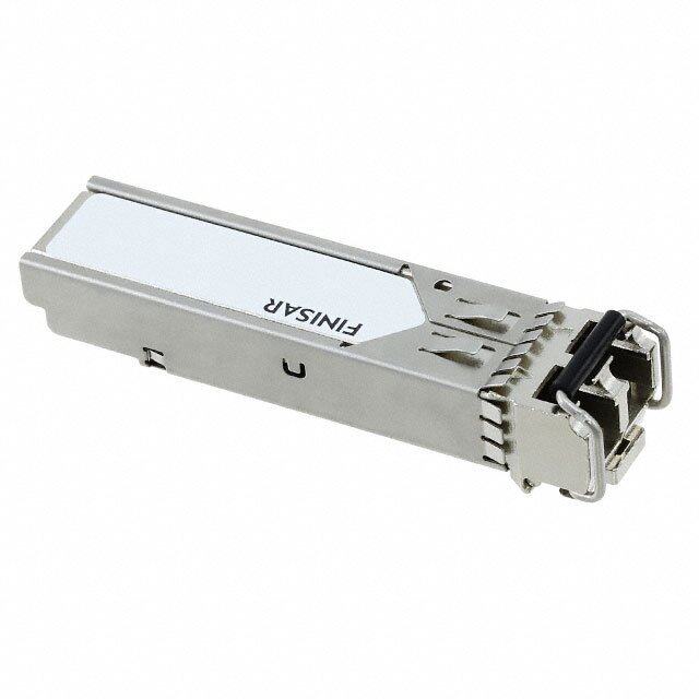
ICGOO电子元器件商城为您提供FTLF8524E2GNL由Finisar设计生产,在icgoo商城现货销售,并且可以通过原厂、代理商等渠道进行代购。 FTLF8524E2GNL价格参考。FinisarFTLF8524E2GNL封装/规格:光纤 - 收发器模块, Fiber Optic Transceiver Module Ethernet 4.25Gbps 850nm 3 V ~ 3.6 V LC Duplex Through Hole。您可以下载FTLF8524E2GNL参考资料、Datasheet数据手册功能说明书,资料中有FTLF8524E2GNL 详细功能的应用电路图电压和使用方法及教程。
Finisar Corporation(现为II-VI Incorporated的一部分)生产的光纤收发器模块型号FTLF8524E2GNL,是一款基于SFP+封装的小型可插拔光模块。该模块主要应用于高速数据传输领域,支持10Gbps的数据速率,适用于以太网、存储区域网络(SAN)、数据中心互联以及电信网络等场景。

 具体应用场景:
1. 数据中心互联
   该模块可用于数据中心之间的短距离或中长距离互联,提供高带宽和低延迟的传输能力,满足云计算、大数据分析和虚拟化技术的需求。

2. 企业级网络
   在企业内部网络中,FTLF8524E2GNL可以用于核心交换机与服务器、存储设备之间的连接,确保高效的数据传输和处理能力。

3. 城域网(MAN)和接入网
   模块支持单模光纤传输,适合城域网中的点对点通信或环网架构,能够覆盖较远的距离(通常可达10公里或更远,具体取决于光模块的规格)。

4. 存储区域网络(SAN)
   在光纤通道(Fibre Channel)环境中,该模块可以实现高性能的存储设备连接,支持关键任务的数据备份和恢复操作。

5. 电信运营商网络
   对于电信运营商而言,FTLF8524E2GNL可用于构建下一代传输网络,例如GPON/EPON升级到更高带宽的解决方案。

 技术特点:
- 支持10GbE标准,兼容IEEE 802.3ae。
- 使用单模光纤(SMF),适合长距离传输。
- 工作波长通常为1310nm,具有较低的功耗和较高的稳定性。
- 热插拔设计,便于维护和升级。

总之,FTLF8524E2GNL是一款性能稳定、应用广泛的光模块,能够在多种网络环境中提供可靠的高速数据传输服务。
| 参数 | 数值 |
| 产品目录 | |
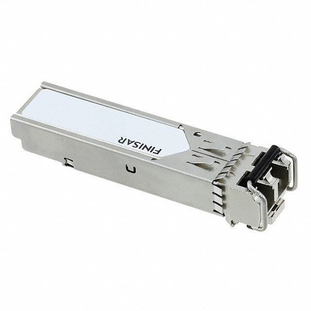
| 描述 | TXRX OPT SFF 4 GB/S 850NM光纤发射器、接收器、收发器 1x/2x/4x FC4.25 Gb/s trnscvr LC conn |
| 产品分类 | 光纤 - 收发器光纤 |
| 品牌 | Finisar Corporation |
| 产品手册 | |
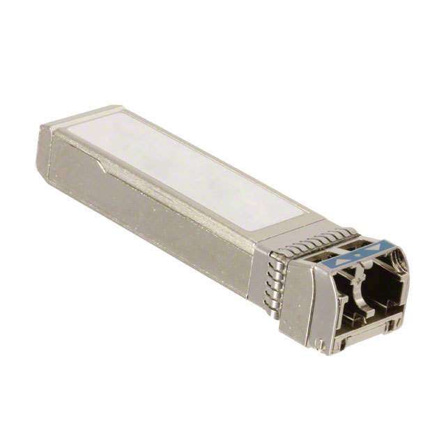
| 产品图片 |
|
| rohs | 符合RoHS无铅 / 符合限制有害物质指令(RoHS)规范要求 |
| 产品系列 | 光纤发射器、接收器、收发器,Finisar FTLF8524E2GNL- |
| mouser_ship_limit | 该产品可能需要其他文件才能进口到中国。 |
| 数据手册 | |
| 产品型号 | FTLF8524E2GNL |
| 产品 | Transceivers |
| 产品目录页面 | |
| 产品种类 | 光纤发射器、接收器、收发器 |
| 其它名称 | 775-1042 |
| 商标 | Finisar |
| 外观尺寸或封装类型 | SFF |
| 安装类型 | 通孔 |
| 安装风格 | Snap In |
| 封装 | Tray |
| 工作电源电压 | 3 V to 3.6 V |
| 工厂包装数量 | 576 |
| 应用 | 以太网 |
| 数据速率 | 4.25Gbps |
| 最大工作温度 | + 85 C |
| 最小工作温度 | - 10 C |
| 标准包装 | 1 |
| 波长 | 850nm |
| 电压-电源 | 3 V ~ 3.6 V |
| 连接器类型 | LC 双工 |


- 商务部:美国ITC正式对集成电路等产品启动337调查
- 曝三星4nm工艺存在良率问题 高通将骁龙8 Gen1或转产台积电
- 太阳诱电将投资9.5亿元在常州建新厂生产MLCC 预计2023年完工
- 英特尔发布欧洲新工厂建设计划 深化IDM 2.0 战略
- 台积电先进制程称霸业界 有大客户加持明年业绩稳了
- 达到5530亿美元!SIA预计今年全球半导体销售额将创下新高
- 英特尔拟将自动驾驶子公司Mobileye上市 估值或超500亿美元
- 三星加码芯片和SET,合并消费电子和移动部门,撤换高东真等 CEO
- 三星电子宣布重大人事变动 还合并消费电子和移动部门
- 海关总署:前11个月进口集成电路产品价值2.52万亿元 增长14.8%


PDF Datasheet 数据手册内容提取
Product Specification 4.25 Gb/s RoHS Compliant Short-Wavelength 2x7 SFF Transceiver FTLF8524E2xNy PRODUCT FEATURES Up to 4.25 Gb/s bi-directional data links 2x7 pin SFF-like footprint Built-in digital diagnostic functions 850nm Oxide VCSEL laser transmitter Duplex LC connector RoHS Compliant and Lead Free Up to 500m on 50/125µm MMF, APPLICATIONS 300m on 62.5/125µm MMF Metal enclosure, for lower EMI Tri-Rate 1.063/2.125/4.25 Gb/s Single 3.3V power supply Fibre Channel Extended operating temperature range: -10°C to 85°C (1) Finisar’s FTLF8524E2xNy Small Form Factor (SFF) transceivers comply with the 2x5 standard package defined by the Small Form Factor Multi-Sourcing Agreement (MSA)1, with the exception of 4 extra pins outlined in Section I below. They are compatible with Fibre Channel FC-PI-2 Rev. 10.02 and are RoHS compliant and lead-free per Directive 2002/95/EC3 and Finisar Application Note AN-2038. PRODUCT SELECTION FTLF8524E2xNy x G 2 Grounding Pins, Short EMI shield K 2 Grounding Pins, Long EMI shield y L Non Rate Selectable - 1x, 2x, 4x Fibre Channel V Rate Selectable - 1x, 2x, 4x Fibre Channel Note 1: For FTLF8524E2KNL only, the standard case operating temperature range is -5°C to +70°C. Finisar Corporation March 15, 2006 RevH Page 1
FTLF8524E2xNy 2x7 Pin SFF Product Specification – March 2006 I. Pin Descriptions Pin Symbol Name/Description Logic Family MS MS Mounting Studs are for mechanical attachment and are connected to NA chassis ground. Chassis ground is internally isolated from circuit grounds. Connection to user’s ground plane is recommended. 1 V Receiver Ground (Common with Transmitter Ground) NA EER 2 V Receiver Power Supply NA CCR 3 SD Signal Detect. Logic 1 indicates normal operation. LVTTL 4 RD- Receiver Inverted DATA out. AC Coupled See Rx spec. 5 RD+ Receiver Non-inverted DATA out. AC Coupled See Rx spec. 6 V Transmitter Power Supply NA CCT 7 V Transmitter Ground (Common with Receiver Ground) NA EET 8 T Transmitter Disable LVTTL DIS 9 TD+ Transmitter Non-Inverted DATA in. AC Coupled. See Tx spec. 10 TD- Transmitter Inverted DATA in. AC Coupled See Tx spec. A SDA Two Wire Digital Diagnostics Data Interface See Note 1 B SCL Two Wire Digital Diagnostics Clock Interface See Note 1 C Rate Open or Low = 1.063 Gb/s or 2.125 Gb/s Fibre Channel, LVTTL Select (Low Bandwidth) See Note 2 High = 2.125 or 4.25 Gb/s Fibre Channel (High Bandwidth) D Reserved NA Notes: 1. Should be pulled up with 4.7k – 10kohms on host board to a voltage between 2.0V and V . CC 2. For Rate Selectable version only: In accordance with SFF Committee SFF-8079 Draft Rev. 1.6, Table 3. Note that rate select can also be set through 2-wire bus in accordance with SFF-84725 at Bit 3, Byte 110, Address A2h (note: writing ‘1’ selects full bandwidth operation). Rate select is the logic OR of the input state of Rate Select Pin and 2-wire bus. Non Rate Selectable version can operate at 1x, 2x, 4x Fibre Channel independent of rate select pin setting. MS D B 10 … 6 TOP VIEW C A 1 … 5 MS Finisar Corporation March 15, 2006 RevH Page 2
FTLF8524E2xNy 2x7 Pin SFF Product Specification – March 2006 II. Absolute Maximum Ratings Parameter Symbol Min Typ Max Unit Ref. Maximum Supply Voltage Vcc -0.5 4.0 V Storage Temperature T -40 85 °C S Case Operating Temperature T -10 85 °C 1 OP Relative Humidity RH 0 85 % 2 Hand Lead Soldering Temperature/Time 260/10 °C/s Wave Lead Soldering Temperature/Time 260/10 °C/s Notes: 1. For FTLF8524E2KNL only, the Case Operating Temperature range is -5°C to +70°C. 2. Non-condensing. III. Electrical Characteristics (T = -10 to 85 °C [see Note 9], V = 3.0 to 3.6 Volts) OP CC Parameter Symbol Min Typ Max Unit Ref. Supply Voltage Vcc 3.0 3.6 V Supply Current Icc 180 240 mA Transmitter Input differential impedance R 80 100 120 Ω 1 in Single ended data input swing Vin,pp 250 1200 mV Transmit Disable Voltage V 2 Vcc V D Transmit Enable Voltage V Vee Vee+ 0.8 V 2 EN Receiver Output differential impedance Rout 80 100 120 Ω 1 Single ended data output swing Vout,pp 250 350 550 mV 3 Data output rise/fall time t/ t 120 ps 4 r f Mask Margin ≤ 2.125 Gb/s 45% Signal Detect Normal SD Vcc V 5 normal HOST Signal Detect Fault SD Vee Vee+0.5 V 5 fault Power Supply Rejection PSR 100 mVpp 6 Deterministic Jitter Contribution @ 2.125 Gb/s RX ∆DJ 51.7 ps 7 Deterministic Jitter Contribution @ 4.25 Gb/s RX ∆DJ 23.5 ps 7 Total Jitter Contribution (p-p) @ 2.125 Gb/s RX ∆TJ 122.4 ps 8 Total Jitter Contribution (p-p) @ 4.25 Gb/s RX ∆TJ 61 ps 8 Notes: 1. AC coupled. 2. Or open circuit. 3. Into 100 Ω differential termination. Data pattern is PRBS 27-1. 4. 20 – 80 %. 5. Signal detect is LVTTL. Logic 1 indicates normal operation; logic 0 indicates no signal detected. 6. All transceiver specifications are compliant with a power supply sinusoidal modulation of 20 Hz to 1.5 MHz up to specified value applied through the power supply filtering network shown on page 23 of the Small Form-factor Pluggable (SFP) Transceiver MultiSource Agreement (MSA), September 14, 2000. 7. Measured with DJ-free data input signal. In actual application, output DJ will be the sum of input DJ and ∆DJ, 10-12 BER. 8. If measured with TJ-free data input signal, , 10-12 BER. In actual application, output TJ will be given by: Finisar Corporation March 15, 2006 RevH Page 3
FTLF8524E2xNy 2x7 Pin SFF Product Specification – March 2006 TJ = DJ +∆DJ + (TJ −DJ )2 +(∆TJ −∆DJ)2 OUT IN IN IN 9. For FTLF8524E2KNL only, Electrical Characteristics apply for T = -5°C to +70°C OP IV. Optical Characteristics (T = -10 to 85 °C [see Note 11], V = 3.0 to 3.6 Volts) OP CC Parameter Symbol Min Typ Max Unit Ref. Transmitter Output Opt. Pwr: 50 or 62.5 MMF P -9 -2.5 dBm 1 OUT Optical Wavelength λ 830 860 nm Spectral Width σ 0.85 nm Optical Modulation Amplitude @ 4.25 Gb/s OMA 247 µW 2 Optical Modulation Amplitude @ 2.125 Gb/s OMA 196 µW 2 Optical Modulation Amplitude @ 1.0625 Gb/s OMA 156 µW 2 Optical Rise/Fall Time t/ t 90 ps 3 r f Relative Intensity Noise RIN -118 dB/Hz Deterministic Jitter Contribution @ 2.125 Gb/s TX ∆DJ 56.5 ps 4 Deterministic Jitter Contribution @ 4.25 Gb/s TX ∆DJ 28.2 ps 4 Total Jitter Contribution @ 2.125 Gb/s TX ∆TJ 119 ps 5 Total Jitter Contribution @ 4.25 Gb/s TX ∆TJ 56.5 ps 5 Mask Margin ≤ 2.125 Gb/s 45% Receiver Receiver Sensitivity = 1.0625 Gb/s Rx -20 dBm 6 SENS Receiver Sensitivity = 2.125 Gb/s Rx -18 dBm 6 SENS Receiver Sensitivity = 4.25 Gb/s Rx -15 dBm 6 SENS Stressed RX sens. =1.0625 Gb/s 0.055 mW 8 Stressed RX sens. =2.125 Gb/s 0.096 mW 8 Stressed RX sens. =4.25 Gb/s 0.138 mW 8 Average Received Power Rx 0 dBm MAX Receiver Elec. 3 dB cutoff frequency 1500 MHz 9 Receiver Elec. 3 dB cutoff frequency 2500 MHz 10 Optical Center Wavelength λ 770 860 nm C Return Loss RL 12 dB Signal Detect Normal SD -20 dBm normal Signal Detect Fault SD -30 dBm fault Signal Detect Hysteresis 0.5 dB Notes: 1. Class 1 Laser Safety per FDA/CDRH, EN (IEC) 60825 laser safety regulations. 2. Equivalent extinction ratio specification for Fibre Channel. Allows smaller ER at higher average power. 3. Unfiltered, 20-80%. Complies with FC 1x and 2x eye mask when filtered. 4. Measured with DJ-free data input signal. In actual application, output DJ will be the sum of input DJ and ∆DJ, 10-12 BER. 5. If measured with TJ-free data input signal, 10-12 BER. In actual application, output TJ will be given by: TJ = DJ +∆DJ + (TJ −DJ )2 +(∆TJ −∆DJ)2 OUT IN IN IN 6. Specifications are for 50 micro-meter or 62.5 micro-meter fiber 7. As measured with 9dB extinction ratio. 8. Measured with conformance signals defined in FC-PI-2 Rev. 10.0 specifications. 9. Rate selectable version in low bandwidth mode. Finisar Corporation March 15, 2006 RevH Page 4
FTLF8524E2xNy 2x7 Pin SFF Product Specification – March 2006 10. Rate selectable version in high bandwidth mode. 11. For FTLF8524E2KNL only, Optical Characteristics apply for T = -5°C to +70°C OP V. General Specifications Parameter Symbol Min Typ Max Units Ref. Data Rate BR 1.062, Gb/sec 1 2.125, 4.25 Bit Error Rate BER 10-12 5 Fiber Length on 50/125µm MMF L 550 m 2 300 3 150 4 Fiber Length on 62.5/125µm MMF L 300 m 2 150 3 70 4 Notes: 1. 1x, 2x, and 4x Fibre Channel compatible per FC-PI-2 Rev. 10.0. 2. At 1.0625 Gb/s Fibre Channel data rate. 3. At 2.125 Gb/s Fibre Channel data rate. 4. At 4.25 Gb/s Fibre Channel data rate. 5. At 1.0625, 2.125, and 4.25Gb/s with PRBS 27-1. VI. Environmental Specifications Finisar SFF transceivers have an extended operating temperature range from –10°C to +85°C case temperature. Parameter Symbol Min Typ Max Units Ref. Case Operating Temperature T -10 85 °C 1 OP Storage Temperature T -40 85 °C S Notes: 1. For FTLF8524E2KNL only, the Case Operating Temperature range is -5°C to +70°C. 2. SFF transceivers may be water washed with the optical port plug in position. However, the process must be followed by a baking step at 80°C for one hour, to ensure the drying of any water which may be trapped inside then shells of the modules. VII. Regulatory Compliance Finisar transceivers are Class 1 Laser Products and comply with US FDA regulations. These products are certified by TÜV and CSA to meet the Class 1 eye safety requirements of EN (IEC) 60825 and the electrical safety requirements of EN (IEC) 60950. Copies of certificates are available at Finisar Corporation upon request. Finisar Corporation March 15, 2006 RevH Page 5
FTLF8524E2xNy 2x7 Pin SFF Product Specification – March 2006 VIII. Digital Diagnostic Functions Finisar FTLF8524E2xNy 2x7 SFF transceivers support a 2-wire serial communication protocol. This interface is identical to the 2-wire serial interface defined in the SFP MSA4, however in this case it is implemented on the 2x7 SFF form factor. The standard SFP serial ID provides access to identification information that describes the transceiver’s capabilities, standard interfaces, manufacturer, and other information. Additionally, an enhanced digital diagnostic monitoring interface is defined, which allows real-time access to device operating parameters such as transceiver temperature, laser bias current, transmitted optical power, received optical power and transceiver supply voltage. It also defines a sophisticated system of alarm and warning flags, which alerts end-users when particular operating parameters are outside of a factory set normal range. In order to access the identification information, the 2x7 SFF transceivers have a 256- byte memory map in E2PROM that is accessible over a 2-wire serial interface at the 8 bit address 1010000X (A0h). The digital diagnostic monitoring interface makes use of the 8 bit address 1010001X (A2h), so the originally defined serial ID memory map remains unchanged. The interface is identical to, and is thus fully backward compatible with both the GBIC Specification and the SFP Multi Source Agreement. Additional information, including details of the electronic interface, is described in Finisar Application Note AN- 2030: “Digital Diagnostics Monitoring Interface for SFP Optical Transceivers”. The operating and diagnostics information is monitored and reported by a Digital Diagnostics Transceiver Controller (DDTC) inside the transceiver, which is accessed through a 2-wire serial interface. When the serial protocol is activated, the serial clock signal (SCL, Mod Def 1) is generated by the host. The positive edge clocks data into the 2x7 SFF transceiver into those segments of the E2PROM that are not write-protected. The negative edge clocks data from the 2x7 SFF transceiver. The serial data signal (SDA, Mod Def 2) is bi-directional for serial data transfer. The host uses SDA in conjunction with SCL to mark the start and end of serial protocol activation. The memories are organized as a series of 8-bit data words that can be addressed individually or sequentially. For more information, please see the SFP MSA documentation4,5 and Finisar Application Note AN-2030. One difference in the implementation of digital diagnostics in the SFF 2x7 form factor from the SFP MSA documentation is the readout of Bit 1, Byte 110 at Address A2h (called “Digital State of the LOS output pin” in the SFP documentation). In the SFF 2x7, the output of this bit is inverted to indicate Signal Detect and match the output of the Signal Detect pin on the SFF part. Digital diagnostics for the FTLF8524E2xNy can be used in host systems that require either internally or externally calibrated digital diagnostics. Finisar Corporation March 15, 2006 RevH Page 6
FTLF8524E2xNy 2x7 Pin SFF Product Specification – March 2006 IX. Mechanical Specifications Finisar’s Small Form Factor (SFF) transceivers comply with the standard dimensions defined by the Small Form Factor Multi-Sourcing Agreement (MSA). FTLF8524E2GNy Finisar Corporation March 15, 2006 RevH Page 7
FTLF8524E2xNy 2x7 Pin SFF Product Specification – March 2006 FTLF8524E2KNy Finisar Corporation March 15, 2006 RevH Page 8
FTLF8524E2xNy 2x7 Pin SFF Product Specification – March 2006 X. PCB Layout and Bezel Recommendations Minimum Recommended Pitch is 0.600” Finisar Corporation March 15, 2006 RevH Page 9
FTLF8524E2xNy 2x7 Pin SFF Product Specification – March 2006 XI. References 1. Small Form Factor (SFF) Transceiver Multi-source Agreement (MSA). July 5, 2000. 2. “Fibre Channel Draft Physical Interface Specification (FC-PI-2 Rev. 10.0)”. American National Standard for Information Systems. 3. Directive 2002/95/EC of the European Council Parliament and of the Council, “on the restriction of the use of certain hazardous substances in electrical and electronic equipment.” January 27, 2003. 4. Small Form-factor Pluggable (SFP) Transceiver Multi-source Agreement (MSA), September 14, 2000. 5. “Digital Diagnostics Monitoring Interface for Optical Transceivers”. SFF Document Number SFF-8472, Revision 9.3. XII. For More Information Finisar Corporation 1389 Moffett Park Drive Sunnyvale, CA 94089-1133 Tel. 1-408-548-1000 Fax 1-408-541-6138 sales@finisar.com www.finisar.com Finisar Corporation March 15, 2006 RevH Page 10
Mouser Electronics Authorized Distributor Click to View Pricing, Inventory, Delivery & Lifecycle Information: F inisar: FTLF8524E2GNL FTLF8524E2KNL