ICGOO在线商城 > 光电元件 > 光纤 - 收发器模块 > FTLF8519P3BTL
 Datasheet下载
- 型号: FTLF8519P3BTL
- 制造商: Finisar
- 库位|库存: xxxx|xxxx
- 要求:
| 数量阶梯 | 香港交货 | 国内含税 |
| +xxxx | $xxxx | ¥xxxx |
查看当月历史价格
查看今年历史价格
FTLF8519P3BTL产品简介:
ICGOO电子元器件商城为您提供FTLF8519P3BTL由Finisar设计生产,在icgoo商城现货销售,并且可以通过原厂、代理商等渠道进行代购。 FTLF8519P3BTL价格参考¥207.61-¥272.31。FinisarFTLF8519P3BTL封装/规格:光纤 - 收发器模块, Fiber Optic Transceiver Module Ethernet 2.125Gbps 850nm 3.3V LC Duplex Pluggable, SFP。您可以下载FTLF8519P3BTL参考资料、Datasheet数据手册功能说明书,资料中有FTLF8519P3BTL 详细功能的应用电路图电压和使用方法及教程。
| 参数 | 数值 |
| 产品目录 | |
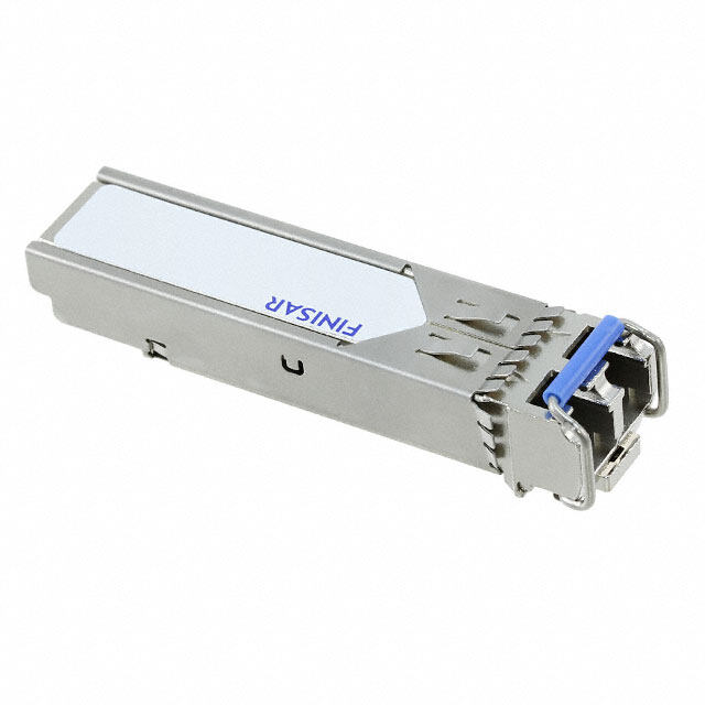
| 描述 | TXRX SFP SGL 2.125GB/S 850NM光纤发射器、接收器、收发器 GigE 1x/2x FC, 2.129 Gb/s trnscvr, 550m |
| 产品分类 | 光纤 - 收发器光纤 |
| 品牌 | Finisar Corporation |
| 产品手册 | |
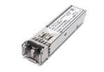
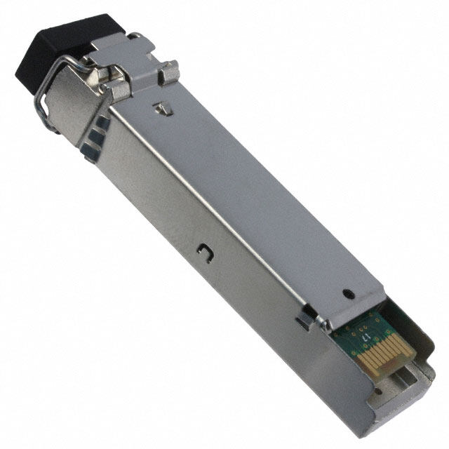
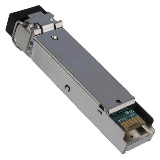
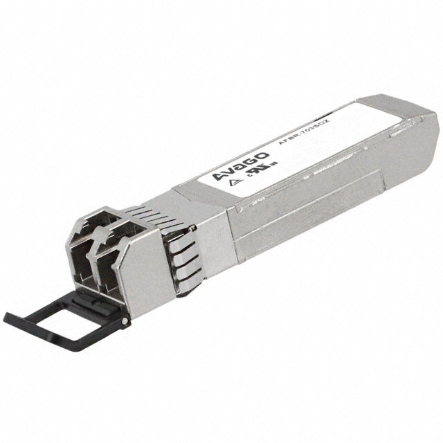
| 产品图片 |
|
| rohs | 符合RoHS无铅 / 符合限制有害物质指令(RoHS)规范要求 |
| 产品系列 | 光纤发射器、接收器、收发器,Finisar FTLF8519P3BTL- |
| mouser_ship_limit | 该产品可能需要其他文档才能发货到中国。 |
| 数据手册 | |
| 产品型号 | FTLF8519P3BTL |
| 产品 | Transceivers |
| 产品种类 | 光纤发射器、接收器、收发器 |
| 其它名称 | 775-1092 |
| 商标 | Finisar |
| 外观尺寸或封装类型 | SFP |
| 安装类型 | 可插入式,SFP |
| 安装风格 | Snap In |
| 封装 | Tray |
| 工作电源电压 | 3.15 V to 3.46 V |
| 工厂包装数量 | 720 |
| 应用 | 以太网 |
| 数据速率 | 2.125 Gb/s |
| 最大工作温度 | + 85 C |
| 最小工作温度 | - 40 C |
| 标准包装 | 30 |
| 波长 | 850nm |
| 电压-电源 | 3.3V |
| 连接器类型 | LC 双工 |


- 商务部:美国ITC正式对集成电路等产品启动337调查
- 曝三星4nm工艺存在良率问题 高通将骁龙8 Gen1或转产台积电
- 太阳诱电将投资9.5亿元在常州建新厂生产MLCC 预计2023年完工
- 英特尔发布欧洲新工厂建设计划 深化IDM 2.0 战略
- 台积电先进制程称霸业界 有大客户加持明年业绩稳了
- 达到5530亿美元!SIA预计今年全球半导体销售额将创下新高
- 英特尔拟将自动驾驶子公司Mobileye上市 估值或超500亿美元
- 三星加码芯片和SET,合并消费电子和移动部门,撤换高东真等 CEO
- 三星电子宣布重大人事变动 还合并消费电子和移动部门
- 海关总署:前11个月进口集成电路产品价值2.52万亿元 增长14.8%


PDF Datasheet 数据手册内容提取
Product Specification 2.125 Gb/s RoHS Compliant Short-Wavelength SFP Transceiver FTLF8519P3ByL PRODUCT FEATURES Up to 2.125 Gb/s bi-directional data links Hot-pluggable SFP footprint Built-in digital diagnostic functions 850nm Oxide VCSEL laser transmitter Duplex LC connector RoHS Compliant and Lead-Free Up to 500m on 50/125m MMF, 300m on 62.5/125m MMF APPLICATIONS Metal enclosure, for lower EMI 1.25 Gb/s 1000Base-SX Ethernet Single 3.3V power supply Dual Rate 1.063/2.125 Gb/s Fibre <500mW power dissipation Channel Industrial operating temperature Wireless – CPRI, OBSAI, LTE range: -40°C to 85°C Finisar’s FTLF8519P3xyL Small Form Factor Pluggable (SFP) transceivers are compatible with the Small Form Factor Pluggable Multi-Sourcing Agreement (MSA)1. They are simultaneously compatible with Gigabit Ethernet as specified in IEEE Std 802.32 and Fibre Channel FC- PI-2 Rev. 5.03. The transceiver is RoHS compliant and per Directive 2011/65/EU4. See Finisar Application Note AN-2038 for more details. . PRODUCT SELECTION FTLF8519P3xyL y N Extended Temperature, -20to 85oC T Industrial Temperature, -40 to 85oC Finisar Corporation August 2015 Rev. D2 Page 1
FTLF8519P3xyL SFP Product Specification I. Pin Descriptions Pin Symbol Name/Description Ref. 1 V Transmitter Ground (Common with Receiver Ground) 1 EET 2 T Transmitter Fault. FAULT 3 T Transmitter Disable. Laser output disabled on high or open. 2 DIS 4 MOD_DEF(2) Module Definition 2. Data line for Serial ID. 3 5 MOD_DEF(1) Module Definition 1. Clock line for Serial ID. 3 6 MOD_DEF(0) Module Definition 0. Grounded within the module. 3 7 Rate Select No connection required 8 LOS Loss of Signal indication. Logic 0 indicates normal operation. 4 9 V Receiver Ground (Common with Transmitter Ground) 1 EER 10 V Receiver Ground (Common with Transmitter Ground) 1 EER 11 V Receiver Ground (Common with Transmitter Ground) 1 EER 12 RD- Receiver Inverted DATA out. AC Coupled 13 RD+ Receiver Non-inverted DATA out. AC Coupled 14 V Receiver Ground (Common with Transmitter Ground) 1 EER 15 V Receiver Power Supply CCR 16 V Transmitter PowerSupply CCT 17 V Transmitter Ground (Common with Receiver Ground) 1 EET 18 TD+ Transmitter Non-Inverted DATA in. AC Coupled. 19 TD- Transmitter Inverted DATA in. AC Coupled. 20 V Transmitter Ground (Common with Receiver Ground) 1 EET Notes: 1. Circuit ground is internally isolated from chassis ground. 2. Laser output disabled on T >2.0V or open, enabled on T <0.8V. DIS DIS 3. Should be pulled up with 4.7k – 10kohms on host board to a voltage between 2.0V and 3.6V. MOD_DEF(0) pulls line low to indicate module is plugged in. 4. LOS is open collector output. Should be pulled up with 4.7k – 10kohms on host board to a voltage between 2.0V and 3.6V. Logic 0 indicates normal operation; logic 1 indicates loss of signal. VeeT 20 1 VeeT TD- 19 2 TXFault TD+ 18 3 TX Disable VeeT 17 4 MOD-DEF(2) VccT 16 Towards 5 MOD-DEF(1) Towards VccR 15 Bezel 6 MOD-DEF(0) ASIC VeeR 14 7 Rate Select RD+ 13 8 LOS RD- 12 9 VeeR VeeR 11 10 VeeR Diagram of Host Board Connector Block Pin Numbers and Names Finisar Corporation August 2015 Rev. D2 Page 2
FTLF8519P3ByL SFP Product Specification II. Absolute Maximum Ratings Parameter Symbol Min Typ Max Unit Ref. Maximum Supply Voltage Vcc -0.5 4.0 V Storage Temperature T -40 85 C S Case Operating Temperature TA -40 85 C Commercial Temperature -5 70 Extended Temperature -20 85 Industrial Temperature -40 85 Relative Humidity RH 0 85 % 1 III. Electrical Characteristics (T , V = 3.15 to 3.46 Volts) A CC Parameter Symbol Min Typ Max Unit Ref. Supply Voltage Vcc 3.15 3.46 V Supply Current Icc 120 144 mA Transmitter Input differential impedance Rin 100 2 Single ended data input swing Vin,pp 250 1200 mV 3 Transmit Disable Voltage V 2 Vcc V 4 D Transmit Enable Voltage V Vee Vee+ 0.8 V EN Receiver Single ended data output swing Vout,pp 250 450 550 mV 5 Data output rise time t 90 175 ps 6 r Data output fall time t 90 175 ps 6 f Mask Margin 45% LOS Fault V 2 Vcc V 7 LOS fault HOST LOS Normal V Vee Vee+0.5 V 7 LOS norm Power Supply Rejection PSR 100 mVpp 8 Deterministic Jitter Contribution RX DJ 51.7 ps 9 Total Jitter Contribution RX TJ <65 122.4 ps 10 Notes: 1. Non condensing. 2. Connected directly to TX data input pins. AC coupling from pins into laser driver IC. 3. We recommend <600mV for best EMI performance. 4. Or open circuit. 5. Into 100 ohms differential termination. 6. 20 – 80 % 7. LOS is an open collector output. Should be pulled up with 4.7k – 10kohms on the host board. Normal operation is logic 0; loss of signal is logic 1. Maximum pull-up voltage is 5.5V. 8. Receiver sensitivity is compliant with power supply sinusoidal modulation of 20 Hz to 1.5 MHz up to specified value applied through the recommended power supply filtering network. 9. Typical peak-to-peak jitter (=6*RMS width of Jitter). 10. Measured with DJ-free data input signal. In actual application, output DJ will be the sum of input DJ and DJ. 11. If measured with TJ-free data input signal. In actual application, output TJ will be given by: TJ DJ DJ TJ DJ 2 TJ DJ2 OUT IN IN IN Finisar Corporation August 2015 Rev. D2 Page 3
FTLF8519P3ByL SFP Product Specification IV. Optical Characteristics (T , V = 3. 15 to 3.46 Volts) A CC Parameter Symbol Min Typ Max Unit Ref. Transmitter Output Opt. Pwr: 50 or 62.5 MMF P -9 -2.5 dBm 1 OUT Optical Wavelength 830 860 nm Spectral Width 0.85 nm Optical Modulation Amplitude @ OMA 196 W 2 2.125 Gb/s Optical Modulation Amplitude @ OMA 156 W 2 1.0625 Gb/s Optical Rise/Fall Time t/ t 100 150 ps 3 r f Relative Intensity Noise RIN -120 dB/Hz Deterministic Jitter Contribution TX DJ 20 56.5 ps 4 Total Jitter Contribution TX TJ <65 119 ps 5 Extinction Ratio @ 1.25 Gb/s ER 9 dB Mask Margin 45% Receiver Receiver Sensitivity = 1.0625 Gb/s RxSENS -18 dBm 6 Receiver Sensitivity = 2.125 Gb/s RxSENS -17 dBm 6 Receiver Sensitivity = 1.25 Gb/s RxSENS -18 dBm 7 Stressed RX sens. =1.0625 Gb/s 0.058 mW 8 Stressed RX sens. =2.125 Gb/s 0.100 mW 8 Stressed RX sens. =1.25 Gb/s -13.5 dBm 9 Average Receiver Power Rx 0 dBm MAX Receiver Elec. 3 dB cutoff freq. 1500 MHz Optical Center Wavelength 770 860 nm C Optical Return Loss 12 dB LOS De-Assert LOS -20 dBm D LOS Assert LOS -30 dBm A LOS Hysteresis 0.5 dB Notes: 1. Class 1 Laser Safety per FDA/CDRH, IEC, and EN60825-1 laser safety standards. 2. Equivalent extinction ratio specification for Fibre Channel. Allows smaller ER at higher average power. 3. Unfiltered, 20-80%. Complies with FC 1x and 2x eye mask when filtered. 4. Measured with DJ-free data input signal. In actual application, output DJ will be the sum of input DJ and DJ. 5. If measured with TJ-free data input signal. In actual application, output TJ will be given by: TJ DJ DJ TJ DJ 2 TJ DJ2 OUT IN IN IN 6. Specifications are for 50 micro-meter or 62.5 micro-meter fiber 7. As measured with 9dB extinction ratio. 8. Measured with conformance signals defined in FC-PI-4 Rev. 6.1 specifications. 9. Measured with conformance signals defined in IEEE 802.3 specifications. Finisar Corporation August 2015 Rev. D2 Page 4
FTLF8519P3ByL SFP Product Specification V. General Specifications Parameter Symbol Min Typ Max Units Ref. Data Rate BR 1.062, Gb/sec 1 1.25, 2.125 Bit Error Rate BER 10-12 4 Fiber Length on 50/125m MMF L 550 m 2 300 3 Fiber Length on 62.5/125m MMF L 300 m 2 150 3 Notes: 1. Gigabit Ethernet and 1x, 2x Fibre Channel compatible, per IEEE 802.3 and FC-PI-2 Rev. 5.0 respectively. 2. At 1.0625 Gb/s Fibre Channel and 1.25 Gb/s Gigabit Ethernet data rates. 3. At 2.125 Gb/s Fibre Channel data rate. 4. 2.125Gb/s with PRBS 27-1. VI. Environmental Specifications Parameter Symbol Min Typ Max Units Ref. Case Operating Temperature T -40 85 °C op Commercial Temperature -5 70 Extended Temperature -20 85 Industrial Temperature -40 85 Storage Temperature T -40 85 °C sto VII. Regulatory Compliance Finisar transceivers are Class 1 Laser Products and comply with US FDA regulations. These products are certified by TÜV and CSA to meet the Class 1 eye safety requirements of EN (IEC) 60825 and the electrical safety requirements of EN (IEC) 60950. Copies of certificates are available at Finisar Corporation upon request. Copies of the referenced certificates are available at Finisar Corporation upon request. Finisar Corporation August 2015 Rev. D2 Page 5
FTLF8519P3ByL SFP Product Specification VIII. Digital Diagnostic Functions Finisar FTLF8519P3xyL SFP transceivers support the 2-wire serial communication protocol as defined in the SFP MSA1. It is very closely related to the E2PROM defined in the GBIC standard, with the same electrical specifications. The standard SFP serial ID provides access to identification information that describes the transceiver’s capabilities, standard interfaces, manufacturer, and other information. Additionally, Finisar SFP transceivers provide a unique enhanced digital diagnostic monitoring interface, which allows real-time access to device operating parameters such as transceiver temperature, laser bias current, transmitted optical power, received optical power and transceiver supply voltage. It also defines a sophisticated system of alarm and warning flags, which alerts end-users when particular operating parameters are outside of a factory set normal range. The SFP MSA defines a 256-byte memory map in E2PROM that is accessible over a 2-wire serial interface at the 8 bit address 1010000X (A0h). The digital diagnostic monitoring interface makes use of the 8 bit address 1010001X (A2h), so the originally defined serial ID memory map remains unchanged. The interface is identical to, and is thus fully backward compatible with both the GBIC Specification and the SFP Multi Source Agreement. The complete interface is described in Finisar Application Note AN- 2030: “Digital Diagnostics Monitoring Interface for SFP Optical Transceivers”. The operating and diagnostics information is monitored and reported by a Digital Diagnostics Transceiver Controller (DDTC) inside the transceiver, which is accessed through a 2-wire serial interface. When the serial protocol is activated, the serial clock signal (SCL, Mod Def 1) is generated by the host. The positive edge clocks data into the SFP transceiver into those segments of the E2PROM that are not write-protected. The negative edge clocks data from the SFP transceiver. The serial data signal (SDA, Mod Def 2) is bi-directional for serial data transfer. The host uses SDA in conjunction with SCL to mark the start and end of serial protocol activation. The memories are organized as a series of 8-bit data words that can be addressed individually or sequentially. For more information, please see the SFP MSA documentation1,5 or Finisar Application Note AN-2030. Please note that evaluation board FDB-1018 is available with Finisar ModDEMO software that allows simple to use communication over the 2-wire serial interface. Finisar Corporation August 2015 Rev. D2 Page 6
FTLF8519P3ByL SFP Product Specification IX. Digital Diagnostic Specifications FTLF8519P2xyL transceivers can be used in host systems that require either internally or externally calibrated digital diagnostics. Parameter Symbol Units Min Max Accuracy Ref. Transceiver temperature D ºC -40 +85 ±5ºC DDTemp Transceiver supply voltage D V 3.0 3.6 ±3% DDVoltage Transmitter bias current D mA 0 20 ±10% 1 DDBias Transmitter output power D dBm -9 -2.5 ±3dB DDTx-Power Receiver average optical input power D dBm -20 0 ±3dB DDRx-Power Notes: 1. Accuracy of Measured Tx Bias Current is 10% of the actual Bias Current from the laser driver to the laser. Finisar Corporation August 2015 Rev. D2 Page 7
FTLF8519P3ByL SFP Product Specification X. Mechanical Specifications Finisar’s Small Form Factor Pluggable (SFP) transceivers are compatible with the dimensions defined by the SFP Multi-Sourcing Agreement (MSA). FTLF8519P3ByL Finisar Corporation August 2015 Rev. D2 Page 8
FTLF8519P3ByL SFP Product Specification XI. PCB Layout and Bezel Recommendations Finisar Corporation August 2015 Rev. D2 Page 9
FTLF8519P3ByL SFP Product Specification Finisar Corporation August 2015 Rev. D2 Page 10
FTLF8519P3ByL SFP Product Specification XII. References 1. Small Form Factor Pluggable (SFP) Transceiver Multi-source Agreement (MSA). September 14, 2000. 2. IEEE Std 802.3, 2002 Edition, Clause 38, PMD Type 1000BASE-SX. IEEE Standards Department, 2002. 3. “Fibre Channel Draft Physical Interface Specification (FC-PI-2 Rev. 5.0)”. American National Standard for Information Systems. 4. Directive 2011/65/EU of the European Council Parliament and of the Council, “on the restriction of the use of certain hazardous substances in electrical and electronic equipment”. 08-June 2011, which supercedes the previous ROHS Directive 2002/95/EC. 5. “Digital Diagnostics Monitoring Interface for Optical Transceivers”. SFF Document Number SFF-8472, Revision 9.3. XIII. For More Information Finisar Corporation 1308 Moffett Park Drive Sunnyvale, CA 94089-1133 Tel. 1-408-548-1000 Fax 1-408-541-6138 sales@finisar.com www.finisar.com Finisar Corporation August 2015 Rev. D2 Page 11