ICGOO在线商城 > 集成电路(IC) > 接口 - 模拟开关,多路复用器,多路分解器 > FSA4157AL6X

 Datasheet下载
- 型号: FSA4157AL6X
- 制造商: Fairchild Semiconductor
- 库位|库存: xxxx|xxxx
- 要求:
| 数量阶梯 | 香港交货 | 国内含税 |
| +xxxx | $xxxx | ¥xxxx |
查看当月历史价格
查看今年历史价格
FSA4157AL6X产品简介:
ICGOO电子元器件商城为您提供FSA4157AL6X由Fairchild Semiconductor设计生产,在icgoo商城现货销售,并且可以通过原厂、代理商等渠道进行代购。 FSA4157AL6X价格参考¥1.84-¥3.74。Fairchild SemiconductorFSA4157AL6X封装/规格:接口 - 模拟开关,多路复用器,多路分解器, 1 Circuit IC Switch 2:1 1.15Ohm 6-MicroPak。您可以下载FSA4157AL6X参考资料、Datasheet数据手册功能说明书,资料中有FSA4157AL6X 详细功能的应用电路图电压和使用方法及教程。
| 参数 | 数值 |
| 产品目录 | 集成电路 (IC)半导体 |
| 描述 | IC SWITCH SPDT 6MICROPAK模拟开关 IC SWITCHES |
| 产品分类 | |
| 品牌 | Fairchild Semiconductor |
| 产品手册 | |
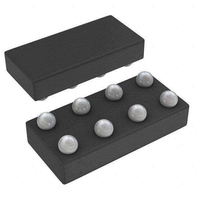
| 产品图片 |
|
| rohs | 符合RoHS无铅 / 符合限制有害物质指令(RoHS)规范要求 |
| 产品系列 | 开关 IC,模拟开关 IC,Fairchild Semiconductor FSA4157AL6X- |
| 数据手册 | |
| 产品型号 | FSA4157AL6X |
| PCN设计/规格 | |
| 产品目录页面 | |
| 产品种类 | 模拟开关 IC |
| 供应商器件封装 | 6-MicroPak |
| 其它名称 | FSA4157AL6XDKR |
| 功能 | |
| 包装 | Digi-Reel® |
| 单位重量 | 19.800 mg |
| 商标 | Fairchild Semiconductor |
| 安装类型 | 表面贴装 |
| 安装风格 | SMD/SMT |
| 导通电阻 | 1.15 欧姆 |
| 导通电阻—最大值 | 4 Ohms |
| 封装 | Reel |
| 封装/外壳 | 6-UFDFN |
| 封装/箱体 | MicroPak-6 |
| 工作温度 | -40°C ~ 85°C |
| 工作电源电压 | - 0.5 V to + 7 V |
| 工厂包装数量 | 5000 |
| 开关配置 | SPDT |
| 最大功率耗散 | 180 mW |
| 最大工作温度 | + 85 C |
| 最小工作温度 | - 40 C |
| 标准包装 | 1 |
| 电压-电源,单/双 (±) | 2.7 V ~ 5.5 V |
| 电压源 | 单电源 |
| 电流-电源 | - |
| 电源电压-最大 | 5.5 V |
| 电源电压-最小 | 2.7 V |
| 电路 | 1 x SPDT |
| 空闲时间—最大值 | 20 ns |
| 系列 | FSA4157A |
| 运行时间—最大值 | 60 ns |
| 零件号别名 | FSA4157AL6X_NL |


- 商务部:美国ITC正式对集成电路等产品启动337调查
- 曝三星4nm工艺存在良率问题 高通将骁龙8 Gen1或转产台积电
- 太阳诱电将投资9.5亿元在常州建新厂生产MLCC 预计2023年完工
- 英特尔发布欧洲新工厂建设计划 深化IDM 2.0 战略
- 台积电先进制程称霸业界 有大客户加持明年业绩稳了
- 达到5530亿美元!SIA预计今年全球半导体销售额将创下新高
- 英特尔拟将自动驾驶子公司Mobileye上市 估值或超500亿美元
- 三星加码芯片和SET,合并消费电子和移动部门,撤换高东真等 CEO
- 三星电子宣布重大人事变动 还合并消费电子和移动部门
- 海关总署:前11个月进口集成电路产品价值2.52万亿元 增长14.8%


PDF Datasheet 数据手册内容提取
Is Now Part of To learn more about ON Semiconductor, please visit our website at www.onsemi.com Please note: As part of the Fairchild Semiconductor integration, some of the Fairchild orderable part numbers will need to change in order to meet ON Semiconductor’s system requirements. Since the ON Semiconductor product management systems do not have the ability to manage part nomenclature that utilizes an underscore (_), the underscore (_) in the Fairchild part numbers will be changed to a dash (-). This document may contain device numbers with an underscore (_). Please check the ON Semiconductor website to verify the updated device numbers. The most current and up-to-date ordering information can be found at www.onsemi.com. Please email any questions regarding the system integration to Fairchild_questions@onsemi.com. ON Semiconductor and the ON Semiconductor logo are trademarks of Semiconductor Components Industries, LLC dba ON Semiconductor or its subsidiaries in the United States and/or other countries. ON Semiconductor owns the rights to a number of patents, trademarks, copyrights, trade secrets, and other intellectual property. A listing of ON Semiconductor’s product/patent coverage may be accessed at www.onsemi.com/site/pdf/Patent-Marking.pdf. ON Semiconductor reserves the right to make changes without further notice to any products herein. ON Semiconductor makes no warranty, representation or guarantee regarding the suitability of its products for any particular purpose, nor does ON Semiconductor assume any liability arising out of the application or use of any product or circuit, and specifically disclaims any and all liability, including without limitation special, consequential or incidental damages. Buyer is responsible for its products and applications using ON Semiconductor products, including compliance with all laws, regulations and safety requirements or standards, regardless of any support or applications information provided by ON Semiconductor. “Typical” parameters which may be provided in ON Semiconductor data sheets and/or specifications can and do vary in different applications and actual performance may vary over time. All operating parameters, including “Typicals” must be validated for each customer application by customer’s technical experts. ON Semiconductor does not convey any license under its patent rights nor the rights of others. ON Semiconductor products are not designed, intended, or authorized for use as a critical component in life support systems or any FDA Class 3 medical devices or medical devices with a same or similar classification in a foreign jurisdiction or any devices intended for implantation in the human body. Should Buyer purchase or use ON Semiconductor products for any such unintended or unauthorized application, Buyer shall indemnify and hold ON Semiconductor and its officers, employees, subsidiaries, affiliates, and distributors harmless against all claims, costs, damages, and expenses, and reasonable attorney fees arising out of, directly or indirectly, any claim of personal injury or death associated with such unintended or unauthorized use, even if such claim alleges that ON Semiconductor was negligent regarding the design or manufacture of the part. ON Semiconductor is an Equal Opportunity/Affirmative Action Employer. This literature is subject to all applicable copyright laws and is not for resale in any manner.
F S A 4 1 March 2014 5 7 , F S A 4 FSA4157, FSA4157A 1 5 7 A Low-Voltage, 1 SPDT Analog Switch — L o w Features Description - V o FSA4157A Features Lower I when the S Input is FSA4157 and FSA4157A are high performance Single lt CC a Lower Than V Pole/Double Throw (SPDT) analog switches. Both g CC devices feature ultra low R of 1.15 maximum at e Maximum 1.15 On Resistance (RON) at 4.5 V VCC 4.5 V VCC and operates oveONr the wide VCC range of , 1 0.3 Maximum R Flatness at 4.5 V V 1.65 V to 5.5 V for FSA4157, and 2.7 V to 5.5 V for ON CC FSA4157A. The device is fabricated with sub-micron Space-Saving 6-lead, MicroPak™ and CMOS technology to achieve fast switching speeds and SP SC70 6 Packages is designed for break-before-make operation. The select D Broad VCC Operating Range: input is TTL level compatible. T A – FSA4157: 1.65 V to 5.5 V The FSA4157A features very low quiescent current even n – FSA4157A: 2.7 V to 5.5 V when the control voltage is lower than the V supply. a CC l Fast Turn-On and Turn-Off Time This feature services the mobile handset applications og very well allowing for the direct interface with baseband Break-Before-Make Enable Circuitry processor general purpose I/Os. Sw Over-Voltage Tolerant TTL-Compatible Control itc Circuitry h Ordering Information Top Part Number Package Description Packing Method Mark FSA4157P6X A57 6-Lead SC70, EIAJ SC88, 1.25 mm Wide 3000 Units Tape and Reel FSA4157L6X EG 6-Lead MicroPak,™ 1.0 mm Wide 5000 Units Tape and Reel FSA4157AP6X B57 6-Lead SC70, EIAJ SC88, 1.25 mm Wide 3000 Units Tape and Reel FSA4157AL6X EU 6-Lead MicroPak™, 1.0 mm Wide 5000 Units Tape and Reel © 2006 Fairchild Semiconductor Corporation www.fairchildsemi.com FSA5147 • FSA4157A Rev. 1.1.1
F S Pin Configurations A 4 1 5 7 , F B1 1 6 S S 1 6 B1 S A 4 1 5 7 GND 2 5 VCC A VCC 2 5 GND — L o w B0 3 4 A -V A 3 4 B0 o l t (TopView) a g (TopThroughView) e , Figure 1. SC70 Pin Assignments Figure 2. MicroPak™ Pin Assignments 1 Pin Definitions S P D Pin# Pin# T Name Description SC70 MicroPak™ A n a 1 6 B1 Data Ports l o 2 5 GND Ground g S 3 4 B0 Data Ports w 4 3 A Data Ports it c h 5 2 V Supply Voltage CC 6 1 S Control Input Truth Table Control Input (S) Function Low B0 connected to A High B1 connected to A © 2006 Fairchild Semiconductor Corporation www.fairchildsemi.com FSA4157 • FSA4157A Rev. 1.1.1 2
F S A Absolute Maximum Ratings 4 1 5 Stresses exceeding the absolute maximum ratings may damage the device. The device may not function or be 7 operable above the recommended operating conditions and stressing the parts to these levels is not recommended. , F In addition, extended exposure to stresses above the recommended operating conditions may affect device reliability. S The absolute maximum ratings are stress ratings only. A 4 1 Symbol Parameter Min. Max. Unit 5 7 VCC Supply Voltage -0.5 6.0 V A V DC Switch Voltage(1) -0.5 V + 0.5 V — S CC V DC Input Voltage(1) -0.5 6.0 V L IN o I DC Input Diode Current -50 mA w IK - I Switch Current 200 mA V SW o ISWPEAK Peak Switch Current (Pulse at 1 ms duration, <10% Duty Cycle) 400 mA lta g SC70 e P Power Dissipation at 85°C 180 mW D , MicroPak™ 1 T Storage Temperature Range -65 +150 °C STG S T Maximum Junction Temperature +150 °C J P D T Lead Temperature (Soldering, 10 seconds) +260 °C L T Human Body Model, A ESD Electrostatic Discharge Capability JESD22-A114 (FSA4157A) 7500 V n a l Note: o g 1. Input and output negative ratings may be exceeded if input and output diode current ratings are observed. S w i t c h Recommended Operating Conditions The Recommended Operating Conditions table defines the conditions for actual device operation. Recommended operating conditions are specified to ensure optimal performance to the datasheet specifications. Fairchild does not recommend exceeding them or designing to Absolute Maximum Ratings. Symbol Parameter Min. Max. Unit FSA4157 1.65 5.50 V Supply Voltage V CC FSA4157A 2.7 5.5 V Control Input Voltage(2) 0 V V CNTRL CC V Switch Input Voltage 0 V V SW CC T Operating Temperature -40 +85 °C A SC70 350 Thermal Resistance in Still Air °C/W JA MicroPak™ (Estimated) 330 Note: 2. Control input must be held HIGH or LOW and it must not float. © 2006 Fairchild Semiconductor Corporation www.fairchildsemi.com FSA4157 • FSA4157A Rev. 1.1.1 3
F S DC Electrical Characteristics A 4 Typical values are at 25°C unless otherwise specified. 15 7 , Ambient Temperature F S Symbol Parameter Conditions V (V) -25° -40 to +85°C Unit A CC 4 1 Min. Typ. Max. Min. Max. 5 7 FSA4157 Only 1.8 to 2.7 1.0 A — V Input Voltage High 2.7 to 3.6 2.0 V IH 4.5 to 5.5 2.4 L o FSA4157 Only 1.8 to 2.7 0.4 w - V FSA4157A Only 2.7 to 3.6 0.4 o V Input Voltage Low V IL 2.7 to 3.6 0.6 lt a g 4.5 to 5.5 0.8 e , Control Input 2.7 to 3.6 -1.0 1.0 1 I V =0 V to V µA IN Leakage IN CC 4.5 to 5.5 -1.0 1.0 S Off Leakage P I , A=1 V, 4.5 V, NO(OFF) Current of Port B0 5.5 ±2 -20 20 nA D I B or B =4.5, 1 V NC(OFF) and B1 0 1 T A On Leakage A=1 V, 4.5v, B0 or n I B =4.5, 1 V,4.5 V or 5.5 ±4 -40 40 nA a A(ON) Current of Port A 1 l Floating o g IOUT=100 mA, 2.7 2.6 4.0 4.3 S Switch On B0 or B1=1.5 V w RON Resistance IOUT=100mA, 4.5 0.95 1.15 1.30 itc B or B =3.5V h 0 1 On Resistance I =100 mA, R Matching Between OUT 4.5 0.06 0.12 0.15 ON B or B =1.5 V Channels(4) 0 1 I =100 mA, B or OUT 0 2.7 1.4 B =0 V, 0.75 V,1.5 V I On Resistance RFLAT(ON) Flatness(4) IOUT=100 mA, B or B =0 V, 1 V, 4.5 0.2 0.3 0.4 0 I 2 V Quiescent Supply V =0 V or V , 3.6 0.1 0.5 1.0 I IN CC µA CC Current IOUT=0 V 5.5 0.1 0.5 1.0 One Input at 2.7 V, Increase in I per others at V or I CC CC 4.3 0.2 10.0 µA CC Input GND (FSA4157A Only) Notes: 3. Measured by the voltage drop between the A and B pins at the indicated current through the switch. On resistance is determined by the lower of the voltage on the two (A or B ports). 4. R = R – R measured at identical V , temperature, and voltage. ON ON max ONmin CC 5. Flatness is defined as the difference between the maximum and minimum value of on resistance over the specified range of conditions. © 2006 Fairchild Semiconductor Corporation www.fairchildsemi.com FSA4157 • FSA4157A Rev. 1.1.1 4
F S AC Electrical Characteristics A 4 Typical values are at 25°C unless otherwise specified. 15 7 , Ambient Temperature F Unit Figure S Symbol Parameter Conditions V (V) -25° -40 to +85°C A CC 4 1 Min. Typ. Max. Min. Max. 5 7 B or B =1.5 V, A 0 1 R =50 , C =35 pF 2.7 to 3.6 60 65 — L L (FSA4157A Only) L t Turn-On B or B =1.5V, ns Figure 8 o ON Time 0 1 2.7 to 3.6 50 60 w R =50, C =35pF L L - V B or B =1.5 V, o 0 1 4.5 to 5.5 35 40 l R =50 , C =35pF t L L a g B or B =1.5 V, 0 1 2.7 to 3.6 20 30 e t Turn-Off RL=50 , CL=35 pF ns Figure 8 , 1 OFF Time B0 or B1=1.5 V, 4.5 to 5.5 15 20 RL=50 , CL=35 pF S P 2.7 to 3.6 Break- FSA4157 D t Before- 4.5 to 5.5 20 ns Figure 9 T BBM Make Time A FSA4157A Only 4.5 to 5.5 25 n a Q Charge CL=1.0 nF, 2.7 to 3.6 10 pC Figure 11 lo Injection VGE=0 V, RGEN=0 4.5 to 5.5 20 g S 2.7 to 3.6 -70 w OIRR Off Isolation f=1 MHz, RL=50 4.5 to 5.5 -70 dB Figure 10 itc h 2.7 to 3.6 -70 Xtalk Crosstalk f=1 MHz, R =50 dB Figure 10 L 4.5 to 5.5 -70 -3db 2.7 to 3.6 300 BW R =50 MHz Figure 13 Bandwidth L 4.5 to 5.5 300 Total 2.7 to 3.6 0.002 R =600 V =0.5, THD Harmon L IN % Figure 14 f=20 Hz to 20 kHz Distortion 4.5 to 5.5 0.002 Capacitance Ambient Temperature -25° Symbol Parameter Conditions V (V) Unit Figure CC Min. Typ. Max. Control Pin Input C f=1 MHz 0 3.5 pF Figure 12 IN Capacitance C B Port Off Capacitance f=1 MHz 4.5 12.0 pF Figure 12 OFF C On Capacitance f=1 MHz 4.5 40.0 pF Figure 12 ON © 2006 Fairchild Semiconductor Corporation www.fairchildsemi.com FSA4157 • FSA4157A Rev. 1.1.1 5
F S A 4 Typical Performance Characteristics 1 5 7 , F 0 S -10 A -20 4 1 -30 5 B) -40 7 d A on ( -50 — solati --6700 L Off I -80 ow -90 - V -100 o -110 l t a -120 g 1 10 100 1,000 e Frequency (MHz) , 1 Figure 3. Off Isolation, V = 2.7 V to 5.5 V CC S P D 0 T -10 A -20 n a -30 l o B) -40 g d n ( -50 S o w solati --6700 itc Off I -80 h -90 -100 -110 -120 1 10 100 1,000 Frequency (MHz) Figure 4. Crosstalk, V = 2.7 V to 5.5 V CC 0 -1 -2 -3 B) d n ( -4 ai G -5 -6 -7 -8 1 10 100 1,000 Frequency (MHz) CL = 0pF, VCC = 2.7V Figure 5. Bandwidth, V = 2.7 V to 5.5 V CC © 2006 Fairchild Semiconductor Corporation www.fairchildsemi.com FSA4157 • FSA4157A Rev. 1.1.1 6
F S A 4 Typical Performance Characteristics (Continued) 1 5 7 , F S A 4 1 2.500 5 7 A –40°C — 2.160 VIN = 1.500V L RON = 2.032 o w 1.819 -V ) o (N 25°C lt RO VIN = 1.500V ag 1.479 RON = 2.161 e , 1 1.139 85°C S P VIN = 1.500V D RON = 2.322 T 0.799 -0.600 0.000 0.600 1.200 1.800 2.400 3.000 A n VIN (V) a l o Figure 6. RON Switch On Resistance, ION = 100 mA, VCC = 2.7 g S w i tc h 1.500 –40°C 1.327 VIN = 3.500V RON = 804.300m 1.154 W) (N 25°C RO VIN = 3.500V 0.981 RON = 999.800m 0.808 85°C VIN = 3.500V RON = 1.182 0.635 -0.960 0.000 0.960 1.920 2.880 3.840 4.800 VIN (V) Figure 7. R Switch On Resistance, I = 100 mA, V = 4.5 V ON ON CC © 2006 Fairchild Semiconductor Corporation www.fairchildsemi.com FSA4157 • FSA4157A Rev. 1.1.1 7
F S A 4 AC Loadings and Waveforms 1 5 7 , F S A 4 VCC t < 2.5ns 1 r 5 VoBr0 B0 or B1 A VOUT CInopnuttrol VVIINNHL 50% tf < 2.5ns 7A — V B1 RL CL L S 50Ω 35Ω tOFF o w V GND SOwutitpcuht oOUT 0.9 x VOUT 0.9 x VOUT -Vo ION lta g e CL Includes Fixture and Stray Capacitance Logic Input Waveforms Inverted for Switches , that have the Opposite Logic Sense 1 Figure 8. Turn On / Off Timing S P D T A n VCC Control a Input VINH 50% lo g V B0 A V VINL S Bn OUT w B1 it S R50LΩ C35LΩ ch Control 0.9 x V CInopnuttrol GND VOUT OUT Input T BB-M C includes fixture and stray capacitance L Figure 9. Break Before Make Timing V 10nF CC Network Analyzer OFF-ISOLATION = 20logVOUT VIN 0 or VCC S VCC A VIN 50Ω 50Ω ON-LOSS = 20logVOUT VIN FSA4157 BBBB 50 OO B1 VOUT MEAS REF CROSSTALK = 20logVVOIUNT GND 50Ω 50Ω Figure 10. Off Isolation and Crosstalk © 2006 Fairchild Semiconductor Corporation www.fairchildsemi.com FSA4157 • FSA4157A Rev. 1.1.1 8
F S A AC Loadings and Waveforms (Continued) 4 1 5 7 VCC , VOUT Δ VOUT FS R B0 or A A GEN B1 4 VOUT IN 1 + CL OFF ON OFF 57 VGE GND S A — ON Control IN OFF OFF L Input Q = (Δ V )(C) o OUT L w - Figure 11. Charge Injection V o l 10nF VCC tag e , 1 A S P D S V Capacitance oINrL T Meter B0 or VINH An B f = 1MHz 1 a l GND o g S w Figure 12. On / Off Capacitance Measurement Setup i t c h 10nF Signal V Generator CC A 0dBm BN Analyzer 50Ω S Logic Input 0V or VCC GND Figure 13. Bandwidth 10nF VIN V CC A Signal BN Analyzer Generator RL S Logic Input 0V or VCC GND Figure 14. Harmonic Distortion © 2006 Fairchild Semiconductor Corporation www.fairchildsemi.com FSA4157 • FSA4157A Rev. 1.1.1 9
None
None
ON Semiconductor and are trademarks of Semiconductor Components Industries, LLC dba ON Semiconductor or its subsidiaries in the United States and/or other countries. ON Semiconductor owns the rights to a number of patents, trademarks, copyrights, trade secrets, and other intellectual property. A listing of ON Semiconductor’s product/patent coverage may be accessed at www.onsemi.com/site/pdf/Patent−Marking.pdf. ON Semiconductor reserves the right to make changes without further notice to any products herein. ON Semiconductor makes no warranty, representation or guarantee regarding the suitability of its products for any particular purpose, nor does ON Semiconductor assume any liability arising out of the application or use of any product or circuit, and specifically disclaims any and all liability, including without limitation special, consequential or incidental damages. Buyer is responsible for its products and applications using ON Semiconductor products, including compliance with all laws, regulations and safety requirements or standards, regardless of any support or applications information provided by ON Semiconductor. “Typical” parameters which may be provided in ON Semiconductor data sheets and/or specifications can and do vary in different applications and actual performance may vary over time. All operating parameters, including “Typicals” must be validated for each customer application by customer’s technical experts. ON Semiconductor does not convey any license under its patent rights nor the rights of others. ON Semiconductor products are not designed, intended, or authorized for use as a critical component in life support systems or any FDA Class 3 medical devices or medical devices with a same or similar classification in a foreign jurisdiction or any devices intended for implantation in the human body. Should Buyer purchase or use ON Semiconductor products for any such unintended or unauthorized application, Buyer shall indemnify and hold ON Semiconductor and its officers, employees, subsidiaries, affiliates, and distributors harmless against all claims, costs, damages, and expenses, and reasonable attorney fees arising out of, directly or indirectly, any claim of personal injury or death associated with such unintended or unauthorized use, even if such claim alleges that ON Semiconductor was negligent regarding the design or manufacture of the part. ON Semiconductor is an Equal Opportunity/Affirmative Action Employer. This literature is subject to all applicable copyright laws and is not for resale in any manner. PUBLICATION ORDERING INFORMATION LITERATURE FULFILLMENT: N. American Technical Support: 800−282−9855 Toll Free ON Semiconductor Website: www.onsemi.com Literature Distribution Center for ON Semiconductor USA/Canada 19521 E. 32nd Pkwy, Aurora, Colorado 80011 USA Europe, Middle East and Africa Technical Support: Order Literature: http://www.onsemi.com/orderlit Phone: 303−675−2175 or 800−344−3860 Toll Free USA/Canada Phone: 421 33 790 2910 Fax: 303−675−2176 or 800−344−3867 Toll Free USA/Canada Japan Customer Focus Center For additional information, please contact your local Email: orderlit@onsemi.com Phone: 81−3−5817−1050 Sales Representative © Semiconductor Components Industries, LLC www.onsemi.com www.onsemi.com 1
Mouser Electronics Authorized Distributor Click to View Pricing, Inventory, Delivery & Lifecycle Information: O N Semiconductor: FSA4157AL6X FSA4157AP6X