ICGOO在线商城 > 集成电路(IC) > PMIC - 配电开关,负载驱动器 > FPF2146
 Datasheet下载
- 型号: FPF2146
- 制造商: Fairchild Semiconductor
- 库位|库存: xxxx|xxxx
- 要求:
| 数量阶梯 | 香港交货 | 国内含税 |
| +xxxx | $xxxx | ¥xxxx |
查看当月历史价格
查看今年历史价格
FPF2146产品简介:
ICGOO电子元器件商城为您提供FPF2146由Fairchild Semiconductor设计生产,在icgoo商城现货销售,并且可以通过原厂、代理商等渠道进行代购。 FPF2146价格参考。Fairchild SemiconductorFPF2146封装/规格:PMIC - 配电开关,负载驱动器, 。您可以下载FPF2146参考资料、Datasheet数据手册功能说明书,资料中有FPF2146 详细功能的应用电路图电压和使用方法及教程。
FPF2146是由ON Semiconductor(安森美半导体)生产的一款PMIC(电源管理集成电路),主要用于配电开关和负载驱动器应用。该器件具有高效、灵活的特性,适用于多种需要精确控制电源分配和负载管理的场景。

 应用场景:

1. 消费电子设备:
   FPF2146广泛应用于智能手机、平板电脑、笔记本电脑等便携式设备中。它能够为这些设备中的多个子系统提供稳定的电源管理,确保每个组件在不同工作状态下都能获得合适的电流和电压,从而提高整体能效并延长电池寿命。

2. 工业自动化:
   在工业控制系统中,FPF2146可用于管理各种传感器、执行器和其他外围设备的电源分配。其高精度的电流和电压控制功能,有助于提升系统的稳定性和可靠性,减少因电源波动导致的故障。

3. 通信基础设施:
   该器件也适用于基站、路由器等通信设备中。通过精确控制电源分配,FPF2146可以确保这些设备在高负荷运行时仍能保持高效能,同时降低功耗,提高散热效率。

4. 汽车电子:
   在现代汽车中,FPF2146可用于管理车载信息娱乐系统、驾驶辅助系统、电动助力转向等关键部件的电源。其低功耗和高可靠性特点,使得它在汽车环境中表现出色,确保车辆各系统的正常运作。

5. 物联网(IoT)设备:
   对于智能家居、智能城市等物联网应用场景,FPF2146能够为各类低功耗传感器节点、网关等设备提供稳定的电源支持。其高效的电源管理能力有助于优化整个物联网系统的能耗,延长设备的工作时间。

总之,FPF2146凭借其出色的电源管理和负载驱动性能,在多个领域中发挥着重要作用,帮助设计者实现更高效、更可靠的电源管理系统。
| 参数 | 数值 |
| 产品目录 | 集成电路 (IC) |
| 描述 | IC LOAD SWITCH REV CURR BK 6-MLP |
| 产品分类 | PMIC - 电源分配开关 |
| 品牌 | Fairchild Semiconductor |
| 数据手册 | |
| 产品图片 |
|
| 产品型号 | FPF2146 |
| PCN设计/规格 | |
| Rds(On) | 160 毫欧 |
| rohs | 无铅 / 符合限制有害物质指令(RoHS)规范要求 |
| 产品系列 | - |
| 产品目录页面 | |
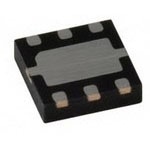
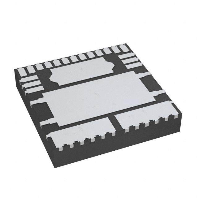
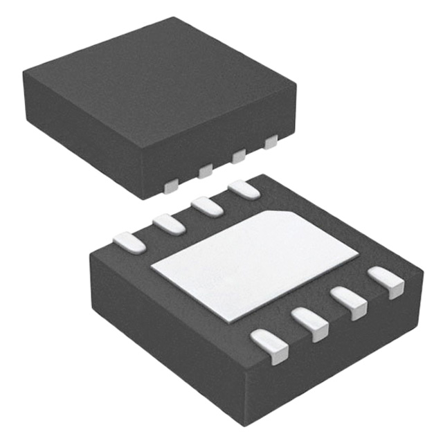
| 供应商器件封装 | 6-MLP(2x2) |
| 其它名称 | FPF2146DKR |
| 内部开关 | 是 |
| 包装 | Digi-Reel® |
| 安装类型 | 表面贴装 |
| 封装/外壳 | 6-WDFN 裸露焊盘 |
| 工作温度 | -40°C ~ 85°C |
| 标准包装 | 1 |
| 电压-输入 | 1.8 V ~ 5.5 V |
| 电流限制 | 400mA |
| 类型 | 高端开关 |
| 输出数 | 1 |


- 商务部:美国ITC正式对集成电路等产品启动337调查
- 曝三星4nm工艺存在良率问题 高通将骁龙8 Gen1或转产台积电
- 太阳诱电将投资9.5亿元在常州建新厂生产MLCC 预计2023年完工
- 英特尔发布欧洲新工厂建设计划 深化IDM 2.0 战略
- 台积电先进制程称霸业界 有大客户加持明年业绩稳了
- 达到5530亿美元!SIA预计今年全球半导体销售额将创下新高
- 英特尔拟将自动驾驶子公司Mobileye上市 估值或超500亿美元
- 三星加码芯片和SET,合并消费电子和移动部门,撤换高东真等 CEO
- 三星电子宣布重大人事变动 还合并消费电子和移动部门
- 海关总署:前11个月进口集成电路产品价值2.52万亿元 增长14.8%


PDF Datasheet 数据手册内容提取
Is Now Part of To learn more about ON Semiconductor, please visit our website at www.onsemi.com Please note: As part of the Fairchild Semiconductor integration, some of the Fairchild orderable part numbers will need to change in order to meet ON Semiconductor’s system requirements. Since the ON Semiconductor product management systems do not have the ability to manage part nomenclature that utilizes an underscore (_), the underscore (_) in the Fairchild part numbers will be changed to a dash (-). This document may contain device numbers with an underscore (_). Please check the ON Semiconductor website to verify the updated device numbers. The most current and up-to-date ordering information can be found at www.onsemi.com. Please email any questions regarding the system integration to Fairchild_questions@onsemi.com. ON Semiconductor and the ON Semiconductor logo are trademarks of Semiconductor Components Industries, LLC dba ON Semiconductor or its subsidiaries in the United States and/or other countries. ON Semiconductor owns the rights to a number of patents, trademarks, copyrights, trade secrets, and other intellectual property. A listing of ON Semiconductor’s product/patent coverage may be accessed at www.onsemi.com/site/pdf/Patent-Marking.pdf. ON Semiconductor reserves the right to make changes without further notice to any products herein. ON Semiconductor makes no warranty, representation or guarantee regarding the suitability of its products for any particular purpose, nor does ON Semiconductor assume any liability arising out of the application or use of any product or circuit, and specifically disclaims any and all liability, including without limitation special, consequential or incidental damages. Buyer is responsible for its products and applications using ON Semiconductor products, including compliance with all laws, regulations and safety requirements or standards, regardless of any support or applications information provided by ON Semiconductor. “Typical” parameters which may be provided in ON Semiconductor data sheets and/or specifications can and do vary in different applications and actual performance may vary over time. All operating parameters, including “Typicals” must be validated for each customer application by customer’s technical experts. ON Semiconductor does not convey any license under its patent rights nor the rights of others. ON Semiconductor products are not designed, intended, or authorized for use as a critical component in life support systems or any FDA Class 3 medical devices or medical devices with a same or similar classification in a foreign jurisdiction or any devices intended for implantation in the human body. Should Buyer purchase or use ON Semiconductor products for any such unintended or unauthorized application, Buyer shall indemnify and hold ON Semiconductor and its officers, employees, subsidiaries, affiliates, and distributors harmless against all claims, costs, damages, and expenses, and reasonable attorney fees arising out of, directly or indirectly, any claim of personal injury or death associated with such unintended or unauthorized use, even if such claim alleges that ON Semiconductor was negligent regarding the design or manufacture of the part. ON Semiconductor is an Equal Opportunity/Affirmative Action Employer. This literature is subject to all applicable copyright laws and is not for resale in any manner.
F P F 2 1 November 2008 4 0 / FPF2140/42/43/44/46/47 4 2 tm /4 Full Function Load Switch with Reverse Current Blocking 3 / 4 4 / Features General Description 4 6 / 4 (cid:132) 1.8 to 5.5V Input Voltage Range The FPF2140/42/43/44/46/47 is a series of load switches which 7 (cid:132) Controlled Turn-On provides full protection to systems and loads which may F (cid:132) 200mA and 400mA Current Limit Options encounter large current conditions. These devices contain a u 0.12Ω current-limited P-channel MOSFET which can operate l (cid:132) Undervoltage Lockout l over an input voltage range of 1.8-5.5V. Internally, current is F (cid:132) Thermal Shutdown prevented from flowing when the MOSFET is off and the output u n (cid:132) <2µA Shutdown Current voltage is higher than the input voltage. Switch control is by a c (cid:132) Auto Restart logic input (ON) capable of interfacing directly with low voltage ti o control signals. Each part contains thermal shutdown protection (cid:132) Fast Current limit Response Time n which shuts off the switch to prevent damage to the part when a (cid:132) 5µs to Moderate Over Currents L continuous over-current condition causes excessive heating. o (cid:132) 30ns to Hard Shorts a When the switch current reaches the current limit, the part d (cid:132) Fault Blanking operates in a constant-current mode to prohibit excessive S (cid:132) Reverse Current Blocking currents from causing damage. For the FPF2140/42/44/46, if w (cid:132) Power Good Function the constant current condition still persists after 30ms, the part it c (cid:132) RoHS Compliant will shut off the switch and pull the fault signal pin (FLAGB) low. h The FPF2140/44 have an auto-restart feature which will turn the w Applications switch on again after 450ms if the ON pin is still active. The i t FPF2142/46 do not have this auto-restart feature so the switch h (cid:132) PDAs will remain off until the ON pin is cycled. For the FPF2143/47, a R (cid:132) Cell Phones current limit condition will immediately pull the fault signal pin e v (cid:132) GPS Devices low and the part will remain in the constant-current mode until e the switch current falls below the current limit. The minimum r (cid:132) MP3 Players s current limit is 200mA for the FPF2140/42/43 while that for the e (cid:132) Digital Cameras FPF2144/46/47 is 400mA. C (cid:132) Peripheral Ports u These parts are available in a space-saving 6 pin 2X2 MLP r (cid:132) Hot Swap Supplies r package. e n t B l o c k i n g Pin 1 BOTTOM TOP Ordering Information Current Limit Auto-Restart Current Limit ON Pin Part Blanking Time Time [mA] Activity [ms] [ms] FPF2140 200/300/400 15/30/60 225/450/900 Active HI FPF2142 200/300/400 15/30/60 NA Active HI FPF2143 200/300/400 0 NA Active HI FPF2144 400/600/800 15/30/60 225/450/900 Active HI FPF2146 400/600/800 15/30/60 NA Active HI FPF2147 400/600/800 0 NA Active HI ©2008 Fairchild Semiconductor Corporation 1 www.fairchildsemi.com FPF2140/42/43/44/46/47 Rev. I
F P Typical Application Circuit F 2 1 4 0 / TO LOAD 4 2 V V IN OUT / 4 FPF2140/2/3/4/6/7 3 / 4 PGOOD FLAGB 4 / OFF ON ON 4 6 GND /4 7 F u l l F u n c t i Functional Block Diagram o n L o a VIN d S w i t UVLO c h w i REVERSE t ON CONTROL CURRENT h LOGIC R BLOCKING e v THERMAL e SHUTDOWN CURRENT rs e LIMIT VOUT C u r FLAGB r e PGOOD n t B l o c k i n g GND 2 www.fairchildsemi.com FPF2140/42/43/44/46/47 Rev. I
F P Pin Configuration F 2 1 4 0 / ON 6 1 PGOOD 4 2 / 4 GND 5 7 2 VIN 3/4 4 / FLAGB 4 3 V 4 OUT 6 / 4 2X2 MicroFET-6 7 F u Pin Description l l F Pin Name Function u n Power Good output: Open drain output which indicate that output voltage has reached c 1 PGOOD 90% of input voltage tio n 2 VIN Supply Input: Input to the power switch and the supply voltage For the IC L 3 V Switch Output: Output of the power switch o OUT a Fault Output: Active LO, open drain output which indicates an over current supply under d 4 FLAGB voltage or over temperature state. S w 5, 7 GND Ground i t c 6 ON ON Control Input h w Absolute Maximum Ratings it h R Parameter Min Max Unit e v VIN, VOUT, ON, FLAGB, PGOOD to GND -0.3 6 V e r Power Dissipation 1.2 W s e Operating and Storage Junction Temperature -65 150 °C C Thermal Resistance, Junction to Ambient 86 °C/W u r r Jedec A114A HBM 4000 V e n Jedec C101C CDM 2000 V t B Electrostatic Discharge Protection Jedec A115 MM 400 V l o Air Discharge 15000 V c IEC 61000-4-2 k Contact Discharge 8000 V in g Recommended Operating Range Parameter Min Max Unit V 1.8 5.5 V IN Ambient Operating Temperature, T -40 85 °C A Electrical Characteristics V = 1.8 to 5.5V, T = -40 to +85°C unless otherwise noted. Typical values are at V = 3.3V and T = 25°C. IN A IN A Parameter Symbol Conditions Min Typ Max Units Basic Operation Operating Voltage V 1.8 5.5 V IN V = 1.8V 40 70 100 IN Quiescent Current I I = 0mA V = 3.3V 75 µA Q OUT IN V = 5.5V 85 120 IN 3 www.fairchildsemi.com FPF2140/42/43/44/46/47 Rev. I
F P F Electrical Characteristics Cont. 2 1 V = 1.8 to 5.5V, T = -40 to +85°C unless otherwise noted. Typical values are at V = 3.3V and T = 25°C. 4 IN A IN A 0 Parameter Symbol Conditions Min Typ Max Units / 4 2 VIN = 3.3V, IOUT = 200mA, TA = 25°C 120 160 /4 3 On-Resistance RON VIN = 3.3V, IOUT = 200mA, TA = 85°C 135 180 mΩ / 4 V = 3.3V, I = 200mA, T = -40°C to +85°C 65 180 4 IN OUT A / 4 ON Input Logic High Voltage VIN = 1.8V 0.8 6 (ON) VIH V = 5.5V 1.4 V /4 IN 7 VIN = 1.8V 0.5 F ON Input Logic Low Voltage V V IL u V = 5.5V 1 IN l l ON Input Leakage VON = VIN or GND -1 1 µA F u V Shutdown Current VON = 0V, VIN = 5.5V, -2 2 µA n IN V = short to GND c OUT t i FLAGB Output Logic Low VIN = 5V, ISINK = 10mA 0.05 0.2 V on Voltage VIN = 1.8V, ISINK = 10mA 0.12 0.3 L o FLAGB Output High Leakage V = V = 5V 1 µA a Current IN ON d S PGOOD Threshold Voltage V = 5.5V 90 % IN w PGOOD Threshold Voltage i 1 % tc Hysteresis h PGOOD Output Logic Low VIN = 5V, ISINK = 10mA 0.05 0.1 V w Voltage VIN = 1.8V, ISINK = 10mA 0.12 0.2 V ith PGOOD Output High Leakage R V = V = 5V 1 µA Current IN ON e v Reverse Block e r s V Shutdown Current VON = 0V, VOUT = 5.5V, -2 2 µA e OUT VIN = short to GND C u Protections r r FPF2140, FPF2142, e 200 300 400 n Current Limit I VIN = 3.3V, FPF2143 mA t LIM VOUT = 3.0V FPF2144, FPF2146, B 400 600 800 l FPF2147 o c Shutdown Threshold T increasing 140 k J i n Thermal Shutdown Return from Shutdown 130 °C g Hysteresis 10 Under Voltage Lockout V V Increasing 1.55 1.65 1.75 V UVLO IN Under Voltage Lockout 50 mV Hysteresis Dynamic Delay On Time td R = 500Ω, C = 0.1µF 25 µs ON L L Delay Off Time td R = 500Ω, C = 0.1µF 45 µs OFF L L V Rise Time t R = 500Ω, C = 0.1µF 10 µs OUT R L L V Fall Time t R = 500Ω, C = 0.1µF 110 µs OUT F L L Over Current Blanking Time t FPF2140, FPF2142, FPF2144, FPF2146 15 30 60 ms BLANK Auto-Restart Time t FPF2140, FPF2144 225 450 900 ms RSTRT V = V = 3.3V. Moderate IN ON 5 µs Short Circuit Response Time Over-Current Condition V = V = 3.3V. Hard Short 30 ns IN ON Note 1: Package power dissipation on 1 square inch pad, 2 oz. copper board. 4 www.fairchildsemi.com FPF2140/42/43/44/46/47 Rev. I
F P Typical Characteristics F 2 1 4 90 110 0 105 /4 85 100 2 NT (uA) 80 NT (uA) 9905 /43/4 RE RE 85 VIN = 5.5V 4 SUPPLY CUR 7705 SUPPLY CUR 67785050 VIN = 3.3VVIN = 1.8V /46/47 65 60 F u 55 l 60 50 l F 1 1.5 2 2.5 3 3.5 4 4.5 5 5.5 6 -40 -15 10 35 60 85 u SUPPLY VOLTAGE (V) T, JUNCTION TEMPERATURE (°C) n J c t i o Figure 1. Quiescent Current vs. Input Voltage Figure 2. Quiescent Current vs. Temperature n L o a d S 1.3 1.2 w i 1.2 1.1 tc V) V) h GE ( 1.1 GE ( 1 w OLTA 1 OLTA 0.9 ith H V 0.9 W V 0.8 R V HIGON 0.8 V LOON0.7 eve 0.7 0.6 rs e 0.6 0.5 C 1.5 2 2.5 3 3.5 4 4.5 5 5.5 6 1.5 2 2.5 3 3.5 4 4.5 5 5.5 6 u SUPPLY VOLTAGE (V) SUPPLY VOLTAGE (V) r r e n t Figure 3. VON High Voltage vs. Input Voltage Figure 4. VON Low Voltage vs. Input Voltage B l o c k i n 200 240 g 190 220 180 200 170 hms)115600 hms)116800 VIN = 1.8V O O m140 m (N130 (N140 RO120 RO120 VIN = 3.3V 110 100 100 90 80 VIN = 5.5V 80 60 1 2 3 4 5 6 -40 -15 10 35 60 85 V, SUPPLY VOLTAGE (V) T, JUNCTION TEMPERATURE (°C) IN J Figure 5. R vs. V Figure 6. R vs. Temperature ON IN ON 5 www.fairchildsemi.com FPF2140/42/43/44/46/47 Rev. I
F P Typical Characteristics F 2 1 4 350 700 0 FPF2140 / 42 / 43 FPF2144 / 46 / 47 /4 300 VIN = 5.5V 600 VIN = 5.5V 2 / RRENT (mA)220500 RRENT (mA)450000 43/44/4 UT CU150 UT CU300 6/4 OUTP100 OUTP200 7 F 50 100 u l l 0 0 F 0 1 2 3 4 5 6 0 1 2 3 4 5 6 u n V - V (V) V - V (V) IN OUT IN OUT c t i o Figure 7. Current Limit vs. Output Voltage Figure 8. Current Limit vs. Output Voltage n L o a d 320 635 S FPF2140 / 42 / 43 630 FPF2144 / 46 / 47 w i 315 625 tc CURRENT LIMIT (mA)333001050 CURRENT LIMIT (mA)556666699001120505050 h with Reve 295 r 585 s 580 e 290 575 C -65 -40 -15 10 35 60 85 110 135 -65 -40 -15 10 35 60 85 110 135 u TJ, JUNCTION TEMPERATURE (°C) TJ, JUNCTION TEMPERATURE (°C) rre n t Figure 9. Current Limit vs. Temperature Figure 10. Current Limit vs. Temperature B l o c k i n 100 1000 g VIN = 3.3 V VIN = 3.3 V RL = 500 Ohms RL= 500 Ohms ME (uS) COUT = 0.1uF tdOFF ES (uS)100 TF TI M N/OFF ALL TI ELAY O tdON RISE / F 10 TR D 10 1 -40 -15 10 35 60 85 -40 -15 10 35 60 85 T, JUNCTION TEMPERATURE (°C) T, JUNCTION TEMPERATURE (°C) J J Figure 11. td / td vs. Temperature Figure 12. T / T vs. Temperature ON OFF RISE FALL 6 www.fairchildsemi.com FPF2140/42/43/44/46/47 Rev. I
F P Typical Characteristics F 2 1 4 33 500 0 / 495 4 32.5 2 490 /4 E (mS)313.52 ME (mS)448805 3/44 ANK TIM 31 TART TI447705 /46/4 BL30.5 RES465 7 460 F 30 u 455 l l 29.5 450 F -40 -15 10 35 60 85 -40 -15 10 35 60 85 u n T, JUNCTION TEMPERATURE (°C) T, JUNCTION TEMPERATURE (°C) J J c t i o Figure 13. T vs. Temperature Figure 14. T vs. Temperature BLANK RESTART n L o a d S CIN = 10µF w C = 0.1µF i OUT t VON CIN = 10µF VON RL = 500Ω ch 2V/DIV COUT = 0.1µF 2V/DIV VIN = 3.3V w R = 500Ω L i t VIN = 3.3V h I I R OUT OUT 10mA/DIV 10mA/DIV e v e VOUT rs 2V/DIV e C u r 100µs/DIV 500ns/DIV re n t Figure 15. tdON Response Figure 16. tdOFF Response B l o c k i n g VIN VIN = VON 2V/DIV 2V/DIV C = 10µF IN V = 3.3V IN IOUT IOUT 5A/DIV 500mA/DIV VOUT CIN = 10µF 2V/DIV V = V = 3.3V IN ON V = GND OUT 20µs/DIV 50µs/DIV Figure 17. Short Circuit Response Time Figure 18. Current Limit Response Time (Output shorted to GND) (Switch is powered into a short) 7 www.fairchildsemi.com FPF2140/42/43/44/46/47 Rev. I
F P Typical Characteristics F 2 1 4 0 VIN VIN /4 2V/DIV 2V/DIV 2 / 4 3 / VON VON 44 2V/DIV 2V/DIV / 4 6 500ImOUAT/D IV CCVIIONNU ==T 31=.0 30µV.F1µF 500ImOUAT/D IV CCVIONU ==T 31=.0 31µV0FµF /47 F VOUT VOUT IN u 2V/DIV 2V/DIV ll F u n 50µs/DIV 50µs/DIV c t i o Figure 19. Current Limit Response Time Figure 20. Current Limit Response Time n (Output is loaded by 2.2Ω, COUT = 0.1µF) (Output is loaded by 2.2Ω, COUT = 10µF) L o a d FPF2140/42/44/46 S VDRV2 w VIN CIN = 10µF 2V/DIV it 5V/DIV C = 0.1µF c OUT h RL = 500Ω VON TBLANK w VON VIN = 5.5V 2V/DIV it 5V/DIV h IOUT R 500mA/DIV e VOUT CIN = 10µF ve 5V/DIV C = 0.1µF r OUT s VOUT RL = 500Ω e PGOOD 2V/DIV VIN = 3.3V C 5V/DIV u 20ms/DIV rr 10µs/DIV e n t Figure 21. PGOOD Response Figure 22. TBLANK Response B l o c k i n g V 2 FPF2140/44 DRV 2V/DIV T RESTART V ON 2V/DIV I OUT 500mA/DIV C = 10µF IN C = 0.1µF OUT VOUT RL = 500Ω 2V/DIV VIN = 3.3V 100ms/DIV Figure 23. T Response RESTART Note 2: V signal forces the device to go into overcurrent condition by loading. DRV 8 www.fairchildsemi.com FPF2140/42/43/44/46/47 Rev. I
F P Description of Operation For preventing the switch from large power dissipation during F 2 heavy load a short circuit detection feature is introduced. Short 1 The FPF2140/42/43/44/46/47 are current limited switches that circuit condition is detected by observing the output voltage. 4 protect systems and loads which can be damaged or disrupted The switch is put into short circuit current limiting mode if the 0 / by the application of high currents. The core of each device is a switch is loaded with a heavy load. When the output voltage 4 2 0.12Ω P-channel MOSFET and a controller capable of drops below VSCTH, short circuit detection threshold voltage, / 4 functioning over a wide input operating range of 1.8-5.5V. The the current limit value re-conditioned and short circuit current 3 controller protects against system malfunctions through current limit value is decreased to 62.5% of the current limit value. This /4 limiting, undervoltage lockout and thermal shutdown. The keeps the power dissipation of the part below a certain limit 4 / current limit is preset for either 200mA or 400mA. even at dead short conditions at 5.5V input voltage. The VSCTH 4 6 value is set to be 1V. At around 1.1V of output voltage the / 4 On/Off Control switch is removed from short circuit current limiting mode and 7 the current limit is set to the current limit value. F The ON pin controls the state of the switch. Activating ON u continuously holds the switch in the on state so long as there is l l no undervoltage on VIN or a junction temperature in excess of Undervoltage Lockout F 140°C. ON is active HI and has a low threshold making it The undervoltage lockout turns-off the switch if the input u n capable of interfacing with low voltage signals. In addition, voltage drops below the undervoltage lockout threshold. With c excessive currents will cause the switch to turn off for FPF2140/ the ON pin active the input voltage rising above the t i o 42 and FPF2144/46. The FPF2140/44 have an Auto-Restart undervoltage lockout threshold will cause a controlled turn-on of n feature which will automatically turn the switch on again after the switch which limits current over-shoots. L 450ms. For the FPF2142/46, the ON pin must be toggled to o turn-on the switch again. With no auto-restart, the FPF2143/47 a Reverse Current Blocking d do not turn off in response to a over current condition but instead remain operating in a constant current mode so long as The entire FPF2140/47 family has a Reverse Current Blocking S ON is active and the thermal shutdown or undervoltage lockout feature that protects input source against current flow from w have not activated. output to input. For a standard USB power design, this is an itc important feature which protects the USB host from being h The ON pin control voltage and VIN pin have independent damaged due to reverse current flow on VBUS. The reverse w recommended operating ranges. The ON pin voltage can be current blocking feature is active when the load switch is turned i t driven by a voltage level higher than the input voltage. off. h R If ON pin is LO and output voltage become greater than input e Fault Reporting voltage, no current can flow from the output to the input . The v e Upon the detection of an over-current, an input undervoltage, or FLAGB operation is independent of the Reverse Current r an over-temperature condition, the FLAGB signals the fault blocking feature and will not report a fault condition if this s e mode by activating LO. For the FPF2140/42/44/46, the FLAGB feature is activated. C goes LO at the end of the blanking time while FLAGB goes LO u immediately for the FPF2143/47. FLAGB remains LO through r the Auto-Restart Time for the FPF2140/44. For the FPF2142/ Thermal Shutdown re 46, FLAGB is latched LO and ON must be toggled to release it. The thermal shutdown protects the die from internally or n t With the FPF2143/47, FLAGB is LO during the faults and externally generated excessive temperatures. During an B immediately returns HI at the end of the fault condition. FLAGB over-temperature condition the FLAGB is activated and the lo is an open-drain MOSFET which requires a pull-up resistor switch is turned-off. The switch automatically turns-on again if c between V and FLAGB. During shutdown, the pull-down on temperature of the die drops below the threshold temperature. k IN i n FLAGB is disabled to reduce current draw from the supply. g Timing Diagram Current Limiting 90% The current limit guarantees that the current through the switch V doesn't exceed a maximum value while not limiting at less than ON 10% a minimum value. For the FPF2140/42/43 the minimum current is 200mA and the maximum current is 400mA and for the FPF2144/46/47 the minimum current is 400mA and the 90% 90% maximum current is 800mA. The FPF2140/42/44/46 have a V OUT 10% 10% blanking time of 30ms, nominally, during which the switch will act as a constant current source. At the end of the blanking time, the switch will be turned-off and the FLAGB pin will tdON tR tdOFF tF activate to indicate that current limiting has occurred. The tON tOFF FPF2143/47 have no current limit blanking period so where: immediately upon a current limit condition FLAGB is activated. tdON = Delay On Time t = V Rise Time These parts will remain in a constant current state until the ON R OUT t = Turn On Time pin is deactivated or the thermal shutdown turns-off the switch. ON td = Delay Off Time OFF t = V Fall Time F OUT t = Turn Off Time OFF 9 www.fairchildsemi.com FPF2140/42/43/44/46/47 Rev. I
F P Application Information F 2 1 Typical Application 4 0 / 4 2 / 4 3 VIN VOUT LOAD /4 4 Typical value = 100KΩ FPF2140/2/3/4/6/7 R1 = 100KΩ /4 Battery 6 1.8V-5.5V PGOOD FLAGB R2 = 499Ω /4 OFF ON ON 7 GND C2 = 0.1µF F C1 = 4.7µF u l l F u n c t i o Input Capacitor n To limit the voltage drop on the input supply caused by transient When using the FPF2142/46 attention must be given to the L in-rush currents when the switch turns-on into a discharged load manual resetting of the part. The junction temperature will only o a capacitor or a short-circuit, a capacitor needs to be placed be allowed to increase to the thermal shutdown threshold. Once d between VIN and GND. A 4.7µF ceramic capacitor, CIN, must be this temperature has been reached, toggling ON will not turn-on S placed close to the VIN pin. A higher value of CIN can be used to the switch until the junction temperature drops. For the w further reduce the voltage drop experienced as the switch is FPF2140/44, a short on the output will cause the part to operate it c turned on into a large capacitive load. in a constant current state dissipating a worst case power as h calculated in (3) until the thermal shutdown activates. It will then w cycle in and out of thermal shutdown so long as the ON pin is i Output Capacitor t active and the short is present. h A 0.1uF capacitor C , should be placed between V and OUT OUT R GND. This capacitor will prevent parasitic board inductances e from forcing VOUT below GND when the switch turns-off. For the Board Layout ve FPF2140/42/44/46, the total output capacitance needs to be r For best performance, all traces should be as short as possible. s kept below a maximum value, C (max), to prevent the part OUT To be most effective, the input and output capacitors should be e from registering an over-current condition and turning-off the placed close to the device to minimize the effects that parasitic C switch. The maximum output capacitance can be determined u trace inductances may have on normal and short-circuit from the following formula, r operation. Using wide traces for V , V and GND will help r (1) IN OUT e COUT(max) = ILIM(max) xV ItNBLANK(min) mcainseim tioz ea mpbaireansti ttihc eermleactl riimcapl eedfafencctes. along with minimizing the nt B The middle pad (pin 7) should be connected to the GND plate lo of PCB for improving thermal performance of the load switch. c k Power Dissipation An improper layout could result higher junction temperature and in triggering the thermal shutdown protection feature. This concern During normal operation as a switch, the power dissipation is g applies specially with FPF2143 and FPF2147 where load switch small and has little effect on the operating temperature of the turns on into an overcurrent condition and switch supplies part. The parts with the higher current limits will dissipate the constant current limit value. In this case power dissipation of the most power and that will only be, (2) switch (P = (V - V ) x I (max)) could exceed the P = (ILIM)2 x RDS = (0.8)2 x 0.12 = 76.8mW maximum DabsoluteIN poweOr UdTissipatLioIMn of 1.2W. If the part goes into current limit the maximum power dissipation will occur when the output is shorted to ground. For the FPF2140/44, the power dissipation will scale by the Auto-Restart Time, t , and the Over Current Blanking Time, RSTRT t , so that the maximum power dissipated is, BLANK t P(max) = BLANK x V (max) x I (max) t + t IN LIM BLANK RSTRT 30 = x 5.5 x 0.8 = 275mW (3) 30 + 450 10 www.fairchildsemi.com FPF2140/42/43/44/46/47 Rev. I
F P Application Notes F 2 1 Startup Power Sequence 4 0 / 4 2 To Load / VIN1 FPF2140/2/ VOUT1 43 3/4/6/7 / 4 V PGOOD 4 IN1 FLAGB /4 OFF ON ON GND 6/ 4 7 100KΩ F u l l F To Load u VIN2 FPF2140/2/ VOUT2 nc 3/4/6/7 t i PGOOD o VIN2 n FLAGB ON GND Lo a d 100KΩ S TP w i t c Power good function in sequential startup. No battery is loaded to the output h w i Power Good Sequential Startup using Power Good t h R FPF214X family has a "Power Good" feature. PGOOD pin is an The power good pin can be connected to another load switch's e open-drain MOSFET which asserts high when the output enable pin to implement sequential startup. PGOOD pin asserts v voltage reaches 90% of the input voltage. low when the load switch is OFF. This feature allows driving a e r subsequent circuit. The above diagram illustrates power good s PGOOD pin requires an external pull up resistor that is e connected to the output voltage when there is no battery in the function in sequential startup. As the VOUT1 of the first load C switch starts to ramp to the 90% of its input voltage the second load side and the logic level of the subsequent controller u permits. This would give logic levels similar to a CMOS output switch remains in OFF state. Whereas the VOUT1 passes the rr 90% threshold, power good signal becomes active and asserts e stage for PGOOD, while still keeping the option to tie the pull-up high. This signal will turn on the second load switch and V n to a different supply voltage. A typical value of 100KΩ is OUT2 t recommended to be used as pull up resistor. The PGOOD pin will start to increase. The total startup time may vary according B to the difference between supply voltages that are used in the l status is independent of the ON pin position. This mean that o application. c PGOOD pin stays low when the load switch is OFF. If the Power k Good feature is not used in the application the pin can be i n connected directly to GND. g 11 www.fairchildsemi.com FPF2140/42/43/44/46/47 Rev. I
0.05 C 2.0 A 1.72 1.68 2X B 6 4 0.15 2.0 0.90 1.21 2.25 0.52(6X) 0.05 C PIN1IDENT 1 3 TOPVIEW 2X 0.65 0.42(6X) RECOMMENDED LANDPATTERN (cid:19)(cid:17)(cid:26)(cid:24)(cid:147)(cid:19)(cid:17)(cid:19)(cid:24) 0.10 C (cid:19)(cid:17)(cid:21)(cid:19)(cid:147)(cid:19)(cid:17)(cid:19)(cid:24) NOTES: 0.08 C SIDEVIEW C (cid:19)(cid:17)(cid:19)(cid:21)(cid:24)(cid:147)(cid:19)(cid:17)(cid:19)(cid:21)(cid:24) A.PACKAGEDOESNOTFULLYCONFORM SEATING TOJEDECMO-229REGISTRATION PLANE B.DIMENSIONSAREINMILLIMETERS. C.DIMENSIONSANDTOLERANCESPER (cid:21)(cid:17)(cid:19)(cid:19)(cid:147)(cid:19)(cid:17)(cid:19)(cid:24) ASMEY14.5M,2009. (cid:20)(cid:17)(cid:23)(cid:19)(cid:147)(cid:19)(cid:17)(cid:19)(cid:24) D.LANDPATTERNRECOMMENDATIONIS (0.70) EXISTINGINDUSTRYLANDPATTERN. PIN1IDENT (0.20)4X E.DRAWINGFILENAME:MKT-MLP06Krev5. 1 3 (cid:19)(cid:17)(cid:22)(cid:21)(cid:147)(cid:19)(cid:17)(cid:19)(cid:24) (0.40) (6X) (cid:19)(cid:17)(cid:27)(cid:19)(cid:147)(cid:19)(cid:17)(cid:19)(cid:24) (0.60) 6 4 (cid:19)(cid:17)(cid:22)(cid:19)(cid:147)(cid:19)(cid:17)(cid:19)(cid:24)(6X) 0.65 0.10 C A B 1.30 0.05 C BOTTOMVIEW
ON Semiconductor and are trademarks of Semiconductor Components Industries, LLC dba ON Semiconductor or its subsidiaries in the United States and/or other countries. ON Semiconductor owns the rights to a number of patents, trademarks, copyrights, trade secrets, and other intellectual property. A listing of ON Semiconductor’s product/patent coverage may be accessed at www.onsemi.com/site/pdf/Patent−Marking.pdf. ON Semiconductor reserves the right to make changes without further notice to any products herein. ON Semiconductor makes no warranty, representation or guarantee regarding the suitability of its products for any particular purpose, nor does ON Semiconductor assume any liability arising out of the application or use of any product or circuit, and specifically disclaims any and all liability, including without limitation special, consequential or incidental damages. Buyer is responsible for its products and applications using ON Semiconductor products, including compliance with all laws, regulations and safety requirements or standards, regardless of any support or applications information provided by ON Semiconductor. “Typical” parameters which may be provided in ON Semiconductor data sheets and/or specifications can and do vary in different applications and actual performance may vary over time. All operating parameters, including “Typicals” must be validated for each customer application by customer’s technical experts. ON Semiconductor does not convey any license under its patent rights nor the rights of others. ON Semiconductor products are not designed, intended, or authorized for use as a critical component in life support systems or any FDA Class 3 medical devices or medical devices with a same or similar classification in a foreign jurisdiction or any devices intended for implantation in the human body. Should Buyer purchase or use ON Semiconductor products for any such unintended or unauthorized application, Buyer shall indemnify and hold ON Semiconductor and its officers, employees, subsidiaries, affiliates, and distributors harmless against all claims, costs, damages, and expenses, and reasonable attorney fees arising out of, directly or indirectly, any claim of personal injury or death associated with such unintended or unauthorized use, even if such claim alleges that ON Semiconductor was negligent regarding the design or manufacture of the part. ON Semiconductor is an Equal Opportunity/Affirmative Action Employer. This literature is subject to all applicable copyright laws and is not for resale in any manner. PUBLICATION ORDERING INFORMATION LITERATURE FULFILLMENT: N. American Technical Support: 800−282−9855 Toll Free ON Semiconductor Website: www.onsemi.com Literature Distribution Center for ON Semiconductor USA/Canada 19521 E. 32nd Pkwy, Aurora, Colorado 80011 USA Europe, Middle East and Africa Technical Support: Order Literature: http://www.onsemi.com/orderlit Phone: 303−675−2175 or 800−344−3860 Toll Free USA/Canada Phone: 421 33 790 2910 Fax: 303−675−2176 or 800−344−3867 Toll Free USA/Canada Japan Customer Focus Center For additional information, please contact your local Email: orderlit@onsemi.com Phone: 81−3−5817−1050 Sales Representative © Semiconductor Components Industries, LLC www.onsemi.com www.onsemi.com 1