ICGOO在线商城 > 隔离器 > 隔离器 - 栅极驱动器 > FOD3180SD
 Datasheet下载
- 型号: FOD3180SD
- 制造商: Fairchild Semiconductor
- 库位|库存: xxxx|xxxx
- 要求:
| 数量阶梯 | 香港交货 | 国内含税 |
| +xxxx | $xxxx | ¥xxxx |
查看当月历史价格
查看今年历史价格
FOD3180SD产品简介:
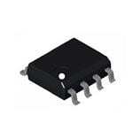
ICGOO电子元器件商城为您提供FOD3180SD由Fairchild Semiconductor设计生产,在icgoo商城现货销售,并且可以通过原厂、代理商等渠道进行代购。 FOD3180SD价格参考。Fairchild SemiconductorFOD3180SD封装/规格:隔离器 - 栅极驱动器, 2.5A Gate Driver 光学耦合 5000Vrms 1 Channel 8-SMD。您可以下载FOD3180SD参考资料、Datasheet数据手册功能说明书,资料中有FOD3180SD 详细功能的应用电路图电压和使用方法及教程。
| 参数 | 数值 |
| 产品目录 | |
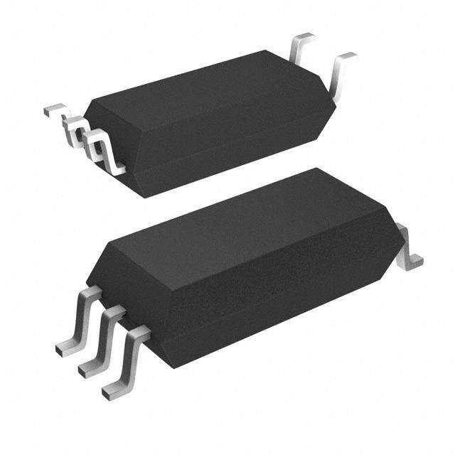
| 描述 | OPTOCOUPLER LOGIC OUT 8-MDIP高速光耦合器 2A IGBT/FET GTE DRV OPTOCOUPLER |
| 产品分类 | 光隔离器 - 栅极驱动器集成电路 - IC |
| 品牌 | Fairchild Semiconductor |
| 产品手册 | |
| 产品图片 |
|
| rohs | 符合RoHS无铅 / 符合限制有害物质指令(RoHS)规范要求 |
| 产品系列 | 光耦合器/光电耦合器,高速光耦合器,Fairchild Semiconductor FOD3180SD- |
| 数据手册 | |
| 产品型号 | FOD3180SD |
| 上升/下降时间(典型值) | 75ns, 55ns |
| 不同If时的传播延迟高-低 | 105ns @ 10mA |
| 产品种类 | 高速光耦合器 |
| 传播延迟tpLH/tpHL(最大值) | 200ns, 200ns |
| 供应商器件封装 | 8-SMD |
| 共模瞬态抗扰度(最小值) | 15kV/µs |
| 其它名称 | FOD3180SDTR |
| 包装 | 带卷 (TR) |
| 单位重量 | 720 mg |
| 商标 | Fairchild Semiconductor |
| 安装类型 | 表面贴装 |
| 封装 | Reel |
| 封装/外壳 | 8-SMD |
| 封装/箱体 | SMD-8 |
| 工作温度 | -40°C ~ 100°C |
| 工厂包装数量 | 1000 |
| 技术 | 光学耦合 |
| 数据速率 | - |
| 最大功率耗散 | 295 mW |
| 最大反向二极管电压 | 5 V |
| 最大工作温度 | + 100 C |
| 最大正向二极管电压 | 1.8 V |
| 最小工作温度 | - 40 C |
| 最小正向二极管电压 | 1.2 V |
| 标准包装 | 1,000 |
| 正向电流 | 25 mA |
| 每芯片的通道数量 | 1 Channel |
| 电压-正向(Vf)(典型值) | 1.43V |
| 电压-电源 | 10 V ~ 20 V |
| 电压-隔离 | 5000Vrms |
| 电流-DC正向(If) | 25mA |
| 电流-峰值输出 | 2.5A |
| 电流-输出/通道 | 2A |
| 电流-输出高,低 | 2A, 2A |
| 系列 | FOD3180 |
| 绝缘电压 | 5000 Vrms |
| 脉宽失真(最大) | 65ns |
| 认可 | cUL,UL |
| 输入类型 | DC |
| 输出类型 | 推挽式/图腾柱 |
| 输出设备 | Phototransistor |
| 通道数 | 1 |


.jpg)


- 商务部:美国ITC正式对集成电路等产品启动337调查
- 曝三星4nm工艺存在良率问题 高通将骁龙8 Gen1或转产台积电
- 太阳诱电将投资9.5亿元在常州建新厂生产MLCC 预计2023年完工
- 英特尔发布欧洲新工厂建设计划 深化IDM 2.0 战略
- 台积电先进制程称霸业界 有大客户加持明年业绩稳了
- 达到5530亿美元!SIA预计今年全球半导体销售额将创下新高
- 英特尔拟将自动驾驶子公司Mobileye上市 估值或超500亿美元
- 三星加码芯片和SET,合并消费电子和移动部门,撤换高东真等 CEO
- 三星电子宣布重大人事变动 还合并消费电子和移动部门
- 海关总署:前11个月进口集成电路产品价值2.52万亿元 增长14.8%


PDF Datasheet 数据手册内容提取
Is Now Part of To learn more about ON Semiconductor, please visit our website at www.onsemi.com Please note: As part of the Fairchild Semiconductor integration, some of the Fairchild orderable part numbers will need to change in order to meet ON Semiconductor’s system requirements. Since the ON Semiconductor product management systems do not have the ability to manage part nomenclature that utilizes an underscore (_), the underscore (_) in the Fairchild part numbers will be changed to a dash (-). This document may contain device numbers with an underscore (_). Please check the ON Semiconductor website to verify the updated device numbers. The most current and up-to-date ordering information can be found at www.onsemi.com. Please email any questions regarding the system integration to Fairchild_questions@onsemi.com. ON Semiconductor and the ON Semiconductor logo are trademarks of Semiconductor Components Industries, LLC dba ON Semiconductor or its subsidiaries in the United States and/or other countries. ON Semiconductor owns the rights to a number of patents, trademarks, copyrights, trade secrets, and other intellectual property. A listing of ON Semiconductor’s product/patent coverage may be accessed at www.onsemi.com/site/pdf/Patent-Marking.pdf. ON Semiconductor reserves the right to make changes without further notice to any products herein. ON Semiconductor makes no warranty, representation or guarantee regarding the suitability of its products for any particular purpose, nor does ON Semiconductor assume any liability arising out of the application or use of any product or circuit, and specifically disclaims any and all liability, including without limitation special, consequential or incidental damages. Buyer is responsible for its products and applications using ON Semiconductor products, including compliance with all laws, regulations and safety requirements or standards, regardless of any support or applications information provided by ON Semiconductor. “Typical” parameters which may be provided in ON Semiconductor data sheets and/or specifications can and do vary in different applications and actual performance may vary over time. All operating parameters, including “Typicals” must be validated for each customer application by customer’s technical experts. ON Semiconductor does not convey any license under its patent rights nor the rights of others. ON Semiconductor products are not designed, intended, or authorized for use as a critical component in life support systems or any FDA Class 3 medical devices or medical devices with a same or similar classification in a foreign jurisdiction or any devices intended for implantation in the human body. Should Buyer purchase or use ON Semiconductor products for any such unintended or unauthorized application, Buyer shall indemnify and hold ON Semiconductor and its officers, employees, subsidiaries, affiliates, and distributors harmless against all claims, costs, damages, and expenses, and reasonable attorney fees arising out of, directly or indirectly, any claim of personal injury or death associated with such unintended or unauthorized use, even if such claim alleges that ON Semiconductor was negligent regarding the design or manufacture of the part. ON Semiconductor is an Equal Opportunity/Affirmative Action Employer. This literature is subject to all applicable copyright laws and is not for resale in any manner.
F O D 3 August 2008 1 8 0 — FOD3180 2 A O 2A Output Current, High Speed MOSFET Gate Driver u t Optocoupler p u t C u Features Description r r e ■ Guaranteed operating temperature range of -40°C to The FOD3180 is a 2A Output Current, High Speed n t +100°C MOSFET Gate Drive Optocoupler. It consists of a , H ■ 2A minimum peak output current aluminium gallium arsenide (AlGaAs) light emitting diode i g ■ High speed response: 200ns max propagation delay optically coupled to a CMOS detector with PMOS and h over temperature range NMOS output power transistors integrated circuit power S ■ 250kHz maximum switching speed stage. It is ideally suited for high frequency driving of p e power MOSFETs used in Plasma Display Panels ■ 30ns typ pulse width distortion e (PDPs), motor control inverter applications and high d ■ Wide VCC operating range: 10V to 20V performance DC/DC converters. M ■ 5000Vrms, 1 minute isolation O ■ Under voltage lockout protection (UVLO) with The device is packaged in an 8-pin dual in-line housing S hysteresis compatible with 260°C reflow processes for lead free F E ■ Minimum creepage distance of 7.0mm solder compliance. T ■ Minimum clearance distance of 7.0mm G ■ C-UL, UL and VDE* approved a t ■ RDS(ON) of 1.5Ω (typ.) offers lower power dissipation e D ■ 15kV/µs minimum common mode rejection r i v Applications e r O ■ Plasma Display Panel p ■ High performance DC/DC convertor t o ■ High performance switch mode power supply c o ■ High performance uninterruptible power supply u p ■ Isolated Power MOSFET gate drive l e *Requires ‘V’ ordering option r Functional Block Diagram Package Outlines FOD3180 NO CONNECTION 1 8 VCC 8 ANODE 2 7 OUTPUT 1 CATHODE 3 6 OUTPUT NO CONNECTION 4 5 VEE 8 8 1 1 Note: A 0.1µF bypass capacitor must be connected between pins 5 and 8. ©2005 Fairchild Semiconductor Corporation www.fairchildsemi.com FOD3180 Rev. 1.0.6
F O Absolute Maximum Ratings (T = 25°C unless otherwise specified) D A 3 Stresses exceeding the absolute maximum ratings may damage the device. The device may not function or be 1 operable above the recommended operating conditions and stressing the parts to these levels is not recommended. 8 0 In addition, extended exposure to stresses above the recommended operating conditions may affect device reliability. — The absolute maximum ratings are stress ratings only. 2 A Symbol Parameter Value Units O u T Storage Temperature -40 to +125 °C STG t p T Operating Temperature -40 to +100 °C u OPR t T Junction Temperature -40 to +125 °C C J u T Lead Solder Temperature 260 for 10 sec. °C r SOL r IF(AVG) Average Input Current(1) 25 mA en t I LED Current Minimum Rate of Rise/Fall 250 ns , F(tr, tf) H IF(TRAN) Peak Transient Input Current (<1µs pulse width, 300pps) 1.0 A ig h V Reverse Input Voltage 5 V R S I “High” Peak Output Current(2) 2.5 A p OH(PEAK) e IOL(PEAK) “Low” Peak Output Current(2) 2.5 A ed V – V Supply Voltage -0.5 to 25 V M CC EE O VO(PEAK) Output Voltage 0 to VCC V S P Output Power Dissipation(4) 250 mW F O E P Total Power Dissipation(5) 295 mW T D G a t e Recommended Operating Conditions D r The Recommended Operating Conditions table defines the conditions for actual device operation. Recommended i v operating conditions are specified to ensure optimal performance to the datasheet specifications. Fairchild does not e r recommend exceeding them or designing to absolute maximum ratings. O p Symbol Parameter Value Units to c V – V Power Supply 10 to 20 V o CC EE u I Input Current (ON) 10 to 16 mA p F(ON) l e V Input Voltage (OFF) -3.0 to 0.8 V r F(OFF) ©2005 Fairchild Semiconductor Corporation www.fairchildsemi.com FOD3180 Rev. 1.0.6 2
F O Electrical-Optical Characteristics (DC) D 3 Over recommended operating conditions unless otherwise specified. 1 8 0 Symbol Parameter Test Conditions Min. Typ.* Max. Unit — IOH High Level Output Current(2)(3) VOH = (VCC – VEE – 1V) 0.5 A 2 A V = (V – V – 3V) 2.0 OH CC EE O IOL Low Level Output Current(2)(3) VOL = (VCC – VEE – 1V) 0.5 A u t V = (V – V – 3V) 2.0 p OL CC EE u VOH High Level Output Voltage(6)(7) IO = -100mA VCC – 0.5 V t C V Low Level Output Voltage(6)(7) I = 100mA V + 0.5 V u OL O EE r r ICCH High Level Supply Current Output Open, 4.8 6.0 mA e I = 10 to 16mA n F t , I Low Level Supply Current Output Open, 5.0 6.0 mA H CCL V = -3.0 to 0.8V ig F h I Threshold Input Current Low to I = 0mA, V > 5V 8.0 mA FLH O O S High p e V Threshold Input Voltage High to Low I = 0mA, V < 5V 0.8 V e FHL O O d VF Input Forward Voltage IF = 10mA 1.2 1.43 1.8 V M ∆V /T Temperature Coefficient of Forward I = 10mA -1.5 mV/°C O F A F S Voltage F E V UVLO Threshold V > 5V, I = 10mA 8.3 V UVLO+ O F T V V < 5V, I = 10mA 7.7 V G UVLO– O F a UVLO UVLO Hysteresis 0.6 V t HYST e BV Input Reverse Breakdown Voltage I = 10µA 5 V D R R r CIN Input Capacitance f = 1MHz, VF = 0V 60 pF iv e *Typical values at T = 25°C r A O p t o c o u p l e r ©2005 Fairchild Semiconductor Corporation www.fairchildsemi.com FOD3180 Rev. 1.0.6 3
F O Switching Characteristics D 3 Over recommended operating conditions unless otherwise specified. 1 8 0 Symbol Parameter Test Conditions Min. Typ.* Max. Unit — tPLH Propagation Delay Time to High Output Level(8) IF = 10mA, 50 135 200 ns 2 tPHL Propagation Delay Time to Low Output Level(8) Rf =g 2=5 100kΩH,z, 50 105 200 ns A O PWD Pulse Width Distortion(9) Duty Cycle = 50%, 65 ns ut p PDD Propagation Delay Difference Between Any Cg = 10nF -90 90 ns u (tPHL – tPLH) Two Parts(10) t C t Rise Time C = 10nF, 75 ns u r L tf Fall Time Rg = 10Ω 55 ns rre n t UVLO Turn On Delay 2.0 µs t UVLO ON , H t UVLO Turn Off Delay 0.3 µs UVLO OFF i g | CM | Output High Level Common Mode Transient T = +25°C, 15 kV/µs h H A Immunity(11) (12) I = 10 to 16mA, S f p V = 1.5kV, CM e V = 20V e CC d | CML | Output Low Level Common Mode Transient TA = +25°C, 15 kV/µs M Immunity(11) (13) Vf = 0V, O V = 1.5kV, S CM F V = 20V CC E T *Typical values at TA = 25°C G a t e D Isolation Characteristics r i v e Symbol Parameter Test Conditions Min. Typ.* Max. Unit r O V Withstand Isolation Voltage(14) (15) T = 25°C, 5000 V p ISO A rms t R.H. < 50%, t = 1min., o II-O ≤ 20µA co u RI-O Resistance (input to output)(15) VI-O = 500V 1011 Ω p l C Capacitance (input to output) Freq. = 1MHz 1 pF e I-O r *Typical values at T = 25°C A ©2005 Fairchild Semiconductor Corporation www.fairchildsemi.com FOD3180 Rev. 1.0.6 4
F O Notes: D 3 1. Derate linearly above +70°C free air temperature at a rate of 0.3mA/°C. 1 2. The output currents I and I are specified with a capacitive current limited load = (3 x 0.01µF) + 0.5Ω, 8 OH OL 0 frequency = 8kHz, 50% DF. — 3. The output currents I and I are specified with a capacitive current limited load = (3 x 0.01µF) + 8.5Ω, OH OL 2 frequency = 8kHz, 50% DF. A O 4. Derate linearly above +87°C, free air temperature at the rate of 0.77mW/°C. Refer to Figure 12. u 5. No derating required across operating temperature range. t p 6. In this test, V is measured with a dc load current of 100mA. When driving capacitive load V will approach V u OH OH CC t as I approaches zero amps. C OH u 7. Maximum pulse width = 1ms, maximum duty cycle = 20%. r r 8. t propagation delay is measured from the 50% level on the falling edge of the input pulse to the 50% level of the e PHL n falling edge of the V signal. t propagation delay is measured from the 50% level on the rising edge of the input t O PLH , H pulse to the 50% level of the rising edge of the V signal. O i g 9. PWD is defined as | tPHL – tPLH | for any given device. h 10. The difference between t and t between any two FOD3180 parts under same test conditions. S PHL PLH p 11. Pin 1 and 4 need to be connected to LED common. e e 12. Common mode transient immunity in the high state is the maximum tolerable dV /dt of the common mode pulse d CM M V to assure that the output will remain in the high state (i.e. V > 10.0V). CM O O 13. Common mode transient immunity in a low state is the maximum tolerable dVCM/dt of the common mode pulse, S F V , to assure that the output will remain in a low state (i.e. V < 1.0V). CM O E 14. In accordance with UL 1577, each optocoupler is proof tested by applying an insulation test voltage > 6000Vrms, T G 60Hz for 1 second (leakage detection current limit I < 5µA). I-O a 15. Device considered a two-terminal device: pins on input side shorted together and pins on output side shorted te together. D r i v e r O p t o c o u p l e r ©2005 Fairchild Semiconductor Corporation www.fairchildsemi.com FOD3180 Rev. 1.0.6 5
F O Typical Performance Curves D 3 1 Fig. 2 Low To High Input Current Threshold 8 0 Fig. 1 Input Forward Current vs. Forward Voltage vs. Ambient Temperature — 100 6 V = 10 to 20V 2 NT VCEEC = 0 A A) 10 RE 5 Output = Open O T (m CUR ut CURREN 1 TA = 100°C TA = -40°C H INPUT OLD (mA) 34 put C D GH u ORWAR 0.1 TA = 25°C W TO HITHRES 2 rren I – FF0.01 – LOH 1 t, Hi FL g I h 0.001 0 S 0.6 0.8 1.0 1.2 1.4 1.6 1.8 2.0 2.2 -40 -20 0 20 40 60 80 100 p e VF – FORWARD VOLTAGE (V) TA – AMBIENT TEMPERATURE (°C) e d M Fig. 3 Output Low Voltage vs. Ambient Temperature Fig. 4 High Output Voltage Drop vs. Ambient Temperature O 0.30 V) 0.00 S VF(OFF) = -3.0V to 0.8V OP ( VCC = 10 to 20V, VEE = 0 FE E (V) 0.25 VIOCUCT == 1100V0 mtoA 20V E DR -0.05 IIFO U=T 1 =0 m-1A0 0to m 1A6mA T G AG VEE = 0 AG a OLT 0.20 OLT -0.10 te W V T V D UT LO 0.15 OUTPU -0.15 rive UTP 0.10 GH -0.20 r O V – OOL 0.05 V) – HICC -0.25 ptoc - H ou O 0.00 V -0.30 p -40 -20 0 20 40 60 80 100 ( -40 -20 0 20 40 60 80 100 le r TA – AMBIENT TEMPERATURE (°C) TA – AMBIENT TEMPERATURE (°C) Fig. 5 Supply Current vs. Ambient Temperature Fig. 6 Supply Current vs. Supply Voltage 6.2 6.2 VCC = 20V, VEE = 0 IF = 10mA (for ICCH) A) 5.8 IIFF == 100mmAA ( f(ofor rI CICCCL)H) A) 5.8 ITFA = = 0 2m5AoC (,f oVrE IEC C=L 0)V m m NT ( 5.4 NT ( 5.4 E E R R Y CUR 5.0 ICCL Y CUR 5.0 ICCL UPPL 4.6 ICCH UPPL 4.6 ICCH S S – – C C C C I 4.2 I 4.2 3.8 3.8 -40 -20 0 20 40 60 80 100 10 12 14 16 18 20 TA – AMBIENT TEMPERATURE (°C) VCC – SUPPLY VOLTAGE (V) ©2005 Fairchild Semiconductor Corporation www.fairchildsemi.com FOD3180 Rev. 1.0.6 6
F O Typical Performance Curves (Continued) D 3 1 Fig. 7 Propagation Delay vs. Load Capacitance Fig. 8 Propagation Delay vs. Forward LED Current 8 0 200 200 — VCC = 20V, VEE = 0 VCC = 20V, VEE = 0 AY (ns) 116800 IfRF =G = 2 =15 010m0 kΩHA,,z C,T DGA .== C 21y50conlCeF = 50% AY (ns) 116800 RfT =AG 2==5 21050 koΩCH,z C, DG .= C 1y0cnleF = 50% 2A Ou N DEL 140 tPHL N DEL 140 tPHL tpu GATIO 120 GATIO 120 t Cu A A r OP tPLH OP tPLH re PR 100 PR 100 n – P – P t, H t 80 t 80 i g h 60 60 S 5 10 15 20 25 6 8 10 12 14 16 p CG – LOAD CAPACITANCE (nF) IF – FORWARD LED CURRENT (mA) ee d Fig. 9 Propagation Delay vs. Series Load Resistance Fig. 10 Propagation Delay vs. Ambient Temperature M O 200 200 S VCC = 20V, VEE = 0 VCC = 20V, VEE = 0 F ns) 180 ICFG = =1 01m0nAF, TA = 25oC s) 180 IRFG = =1 01m0ΩA, CG = 10nF ET LAY ( 160 f = 250 kHz, D. Cycle = 50% AY (n 160 f = 250kHz, D. Cycle = 50% Ga ON DE 140 N DEL 140 te D GATI tPHL ATIO tPHL riv PA 120 AG 120 e t – PROP 100 tPLH – PROPP 100 tPLH r Opto 80 t 80 c o u 60 60 p l 10 20 30 40 50 -40 -20 0 20 40 60 80 100 e r RG – SERIES LOAD RESISTANCE (Ω) TA – AMBIENT TEMPERATURE (°C) Fig. 11 Propagation Delay vs. Supply Voltage 180 IF = 10mA, TA = 25oC 160 RG = 10Ω, CG = 10nF s) f = 250 kHz, D. Cycle = 50% n Y ( ELA 140 tPHL D N O TI 120 A AG tPLH OP 100 R P – P 80 t 60 10 15 20 25 VCC – SUPPLY VOLTAGE (V) ©2005 Fairchild Semiconductor Corporation www.fairchildsemi.com FOD3180 Rev. 1.0.6 7
F O Ordering Information D 3 1 Order Entry Identifier 8 0 Option (Example) Description — No option FOD3180 Standard Through Hole Device 2 A S FOD3180S Surface Mount, Lead Bend O SD FOD3180SD Surface Mount, Tape and Reel u t T FOD3180T 0.4" Lead Spacing p u t V FOD3180V VDE 0884 C TV FOD3180TV VDE 0884, 0.4" Lead Spacing u r r SV FOD3180SV VDE 0884, Surface Mount e n SDV FOD3180SDV VDE 0884, Surface Mount, Tape and Reel t, H i g h S Marking Information p e e d M O S 1 F E T 3180 2 G a t e V XX YY B 6 D r i v e r 3 4 5 O p t o c o u Definitions p l e 1 Fairchild logo r 2 Device number 3 VDE mark (Note: Only appears on parts ordered with VDE option – See order entry table) 4 Two digit year code, e.g., ‘03’ 5 Two digit work week ranging from ‘01’ to ‘53’ 6 Assembly package code ©2005 Fairchild Semiconductor Corporation www.fairchildsemi.com FOD3180 Rev. 1.0.6 8
F O Carrier Tape Specifications D 3 1 D 8 0 0 P0 P2 — t E K 0 2 A O u F t p A 0 u W1 B0 W t C u r r e n t UserDirectionofFeed P , H d D 1 i g h S Symbol Description Dimension in mm p e e W Tape Width 16.0 ± 0.3 d t Tape Thickness 0.30 ± 0.05 M O P0 Sprocket Hole Pitch 4.0 ± 0.1 S F D0 Sprocket Hole Diameter 1.55 ± 0.05 E T E Sprocket Hole Location 1.75 ± 0.10 G F Pocket Location 7.5 ± 0.1 a t e P2 4.0 ± 0.1 D P Pocket Pitch 12.0 ± 0.1 r i v A Pocket Dimensions 10.30 ±0.20 e 0 r B 10.30 ±0.20 O 0 p K 4.90 ±0.20 t 0 o c W Cover Tape Width 1.6 ± 0.1 1 o u d Cover Tape Thickness 0.1 max p l Max. Component Rotation or Tilt 10° e r R Min. Bending Radius 30 ©2005 Fairchild Semiconductor Corporation www.fairchildsemi.com FOD3180 Rev. 1.0.6 9
F O Reflow Profile D 3 1 8 245 C, 10–30 s 0 300 — 250 260 C peak 2 C) A e (° 200 O ur 150 u at t per 100 Time above 183 C, <160 sec pu m t Te 50 Ramp up = 2–1 0C/sec C u 0 rr 0 0.5 1 1.5 2 2.5 3 3.5 4 4.5 e n Time (Minute) t , • Peak reflow temperature: 2 60C (package surface temperature) H • Time of temperature higher than 1 83C for 160 seconds or less ig • One time soldering reflow is recommended h S p Output Power Derating e e d The maximum package power dissipation is 295mW. The The output power is the product of the average output M package is limited to this level to ensure that under normal current squared times the output transistor’s RDS(ON): O operating conditions and over extended temperature S P = I 2 • R range that the semiconductor junction temperatures do O(AVG) O(AVG) DS(ON) F not exceed 125°C. The package power is composed of The I is the product of the duty factor times the E O(AVG) T three elements; the LED, static operating power of the peak current flowing in the output. The duty factor is G output IC, and the power dissipated in the output power the ratio of the ‘on’ time of the output load current divided a M25O0SmFWE.T T thraisn psoiswtoerrs .is T dhivei dpeodw beer trwaetinegn tohfe t hseta otiuc tppouwt IeCr oisf by the period of the operating frequency. An RDS(ON) of te 2.0Ω results in an average output load current of 200mA. D the integrated circuit, which is the product of I times the DD The load duty factor is a ratio of the average output time r power supply voltage (V – V ). The maximum IC i DD EE v static output power is 150mW, (V – V ) = 25V, I = of the power MOSFET load circuit and period of the driv- e DD EE DD 6mA. This maximum condition is valid over the opera- ing frequency. r O tional temperature range of -40°C to +100°C. Under these The maximum permissible, operating frequency is deter- p maximum operating conditions, the output of the power t mined by the load supplied to the output at its resulting o MOSFET is allowed to dissipate 100mW of power. output pulse width. Figure 13 shows an example of a c o The absolute maximum output power dissipation versus 0.03µF gate to source capacitance with a series resis- u ambient temperature is shown in Figure 12. The output tance of 8.50Ω. This reactive load results in a composite p l driver is capable of supplying 100mW of output power average pulse width of 1.5µs. Under this load condition it er over the temperature range from -40°C to 87°C. The out- is not necessary to derate the absolute maximum output put derates to 90mW at the absolute maximum operating current until the frequency of operation exceeds 63kHz. temperature of 100°C. Fig. 13 Output Current Derating vs. Frequency Fig. 12 Absolute Maximum Power Dissipation 2.5 vs. Ambient Temperature 0.15 VDD – VEE = Max. = 25V ILDEDD = P 6omwAer = 45mW T (A) 2 N W) RE N ( UR 1.5 O 0.1 C TA = -40°C to 100°C TI T Load = .03µF +8.5Ω A U R DISSIP AK OUTP 1 LOVIFED u=DDt p 1 =uD2 t2um P0tyAuV lFsaec Wtoird t=h 5=0 1%.5µs E E W 0.05 P O – 0.5 P O I 0 1 10 100 0 F – FREQUENCY (kHz) -40 -20 0 20 40 60 80 100 TA – AMBIENT TEMPERATURE (°C) ©2005 Fairchild Semiconductor Corporation www.fairchildsemi.com FOD3180 Rev. 1.0.6 10
F O I and I Test Conditions D OH OL 3 1 This device is tested and specified when driving a com- Figure 14 illustrates the relationship of the LED input 8 plex reactive load. The load consists of a capacitor in the drive current and the device’s output voltage and sourc- 0 series with a current limiting resistor. The capacitor rep- ing and sinking currents. The 0.03µF capacitor load rep- — resents the gate to source capacitance of a power resents the gate to source capacitance of a very large 2 MOSFET transistor. The test load is a 0.03µF capacitor power MOSFET transistor. A single supply voltage of A in series with an 8.5Ω resistor. The LED test frequency is 20V is used in the evaluation. O u 10.0kHz with a 50% duty cycle. The combined I and OH Figure 15 shows the test schematic to evaluate the out- t p I output load current duty factor is 0.6% at the test OL put voltage and sourcing and sinking capability of the u frequency. t device. The I and I are measured at the peak of OH OL C their respective current pulses. u r r e n t , H IF = 8mA ig OFF h LED ON S p e 20V e d OUTPUT P-Channel (ON) N-Channel (ON) M 0 O IOH = 2.2A S F E Load T Current G IOL = 2.2A a t e D r 1µs/Div iv e r Figure 14. FOD 3180 Output Current and Output Voltage vs. LED Drive O p t o c o u p l e r Pulse Generator FOD3180 1 8 0.1µF VO IOMON 2 7 0.33µF IF MON 3 6 8.5Ω 22µF 100Ω 100Ω 4 5 Figure 15. Test Schematic ©2005 Fairchild Semiconductor Corporation www.fairchildsemi.com FOD3180 Rev. 1.0.6 11
None
None
None
None
ON Semiconductor and are trademarks of Semiconductor Components Industries, LLC dba ON Semiconductor or its subsidiaries in the United States and/or other countries. ON Semiconductor owns the rights to a number of patents, trademarks, copyrights, trade secrets, and other intellectual property. A listing of ON Semiconductor’s product/patent coverage may be accessed at www.onsemi.com/site/pdf/Patent−Marking.pdf. ON Semiconductor reserves the right to make changes without further notice to any products herein. ON Semiconductor makes no warranty, representation or guarantee regarding the suitability of its products for any particular purpose, nor does ON Semiconductor assume any liability arising out of the application or use of any product or circuit, and specifically disclaims any and all liability, including without limitation special, consequential or incidental damages. Buyer is responsible for its products and applications using ON Semiconductor products, including compliance with all laws, regulations and safety requirements or standards, regardless of any support or applications information provided by ON Semiconductor. “Typical” parameters which may be provided in ON Semiconductor data sheets and/or specifications can and do vary in different applications and actual performance may vary over time. All operating parameters, including “Typicals” must be validated for each customer application by customer’s technical experts. ON Semiconductor does not convey any license under its patent rights nor the rights of others. ON Semiconductor products are not designed, intended, or authorized for use as a critical component in life support systems or any FDA Class 3 medical devices or medical devices with a same or similar classification in a foreign jurisdiction or any devices intended for implantation in the human body. Should Buyer purchase or use ON Semiconductor products for any such unintended or unauthorized application, Buyer shall indemnify and hold ON Semiconductor and its officers, employees, subsidiaries, affiliates, and distributors harmless against all claims, costs, damages, and expenses, and reasonable attorney fees arising out of, directly or indirectly, any claim of personal injury or death associated with such unintended or unauthorized use, even if such claim alleges that ON Semiconductor was negligent regarding the design or manufacture of the part. ON Semiconductor is an Equal Opportunity/Affirmative Action Employer. This literature is subject to all applicable copyright laws and is not for resale in any manner. PUBLICATION ORDERING INFORMATION LITERATURE FULFILLMENT: N. American Technical Support: 800−282−9855 Toll Free ON Semiconductor Website: www.onsemi.com Literature Distribution Center for ON Semiconductor USA/Canada 19521 E. 32nd Pkwy, Aurora, Colorado 80011 USA Europe, Middle East and Africa Technical Support: Order Literature: http://www.onsemi.com/orderlit Phone: 303−675−2175 or 800−344−3860 Toll Free USA/Canada Phone: 421 33 790 2910 Fax: 303−675−2176 or 800−344−3867 Toll Free USA/Canada Japan Customer Focus Center For additional information, please contact your local Email: orderlit@onsemi.com Phone: 81−3−5817−1050 Sales Representative © Semiconductor Components Industries, LLC www.onsemi.com www.onsemi.com 1
Mouser Electronics Authorized Distributor Click to View Pricing, Inventory, Delivery & Lifecycle Information: O N Semiconductor: FOD3180SDV FOD3180SV FOD3180 FOD3180SD FOD3180TV FOD3180S FOD3180TSV