 Datasheet下载
- 型号: FNC42060F2
- 制造商: Fairchild Semiconductor
- 库位|库存: xxxx|xxxx
- 要求:
| 数量阶梯 | 香港交货 | 国内含税 |
| +xxxx | $xxxx | ¥xxxx |
查看当月历史价格
查看今年历史价格
FNC42060F2产品简介:
ICGOO电子元器件商城为您提供FNC42060F2由Fairchild Semiconductor设计生产,在icgoo商城现货销售,并且可以通过原厂、代理商等渠道进行代购。 FNC42060F2价格参考¥93.50-¥134.16。Fairchild SemiconductorFNC42060F2封装/规格:功率驱动器模块, Power Driver Module IGBT 3 Phase 600V 20A 26-PowerDIP Module (1.024", 26.00mm)。您可以下载FNC42060F2参考资料、Datasheet数据手册功能说明书,资料中有FNC42060F2 详细功能的应用电路图电压和使用方法及教程。
FNC42060F2 是 ON Semiconductor(安森美半导体)推出的一款功率驱动器模块,属于其 FDMF 系列。该模块主要应用于电机驱动、工业自动化以及家电控制等领域,以下是其具体应用场景:

1. 家用电器:
   FNC42060F2 可用于驱动家用电器中的直流无刷电机(BLDC),如空调风扇、冰箱压缩机、洗衣机滚筒等。它能够提供高效、可靠的电机控制性能,支持变频调速功能,从而实现节能和静音效果。

2. 工业设备:
   在工业自动化领域,该模块适用于各种小型到中型电机驱动系统,例如泵、风扇、传送带等设备的控制。它支持三相 BLDC 电机驱动,能够满足工业级应用对可靠性和效率的要求。

3. 电动工具:
   FNC42060F2 可用于便携式或固定式电动工具中,如电钻、电锯等。其高集成度设计简化了电路板布局,同时提供了稳定的电流驱动能力,确保工具在不同负载条件下的平稳运行。

4. 电动车与两轮车:
   该模块还可应用于低功率电动车(如电动滑板车、自行车)的电机控制系统中,为车辆提供高效的能源利用和稳定的动力输出。

5. 散热风扇:
   在计算机散热系统或服务器冷却装置中,FNC42060F2 能够驱动智能 PWM 控制的风扇,根据温度变化动态调整转速,降低功耗并减少噪音。

 产品特点:
- 集成三相半桥驱动器,内置 MOSFET 和驱动 IC。
- 支持高达 42V 的工作电压和 60A 的峰值电流。
- 内置多重保护功能,包括过流保护、过温保护和欠压锁定。
- 小型化封装(如 F2PAK-7L),便于 PCB 布局和散热管理。

综上所述,FNC42060F2 是一款专为中小型电机驱动设计的功率模块,广泛适用于需要高效、紧凑和可靠解决方案的应用场景。
| 参数 | 数值 |
| 产品目录 | |
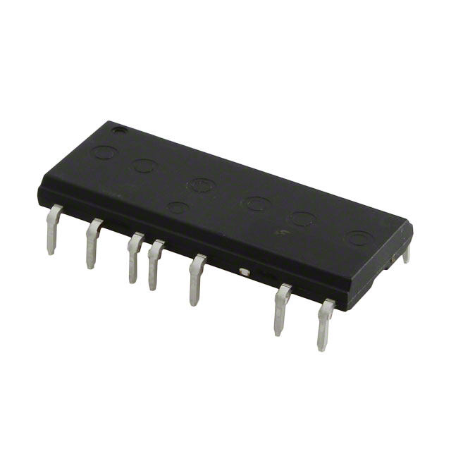
| 描述 | MODULE SPM 45 20A LONG LD马达/运动/点火控制器和驱动器 Motion SPM 45 Series |
| 产品分类 | 功率驱动器 - 模块集成电路 - IC |
| 品牌 | Fairchild Semiconductor |
| 产品手册 | |
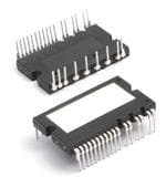
| 产品图片 |
|
| rohs | 符合RoHS无铅 / 符合限制有害物质指令(RoHS)规范要求 |
| 产品系列 | 电源管理 IC,马达/运动/点火控制器和驱动器,Fairchild Semiconductor FNC42060F2Motion-SPM® |
| 数据手册 | |
| 产品型号 | FNC42060F2 |
| PCN封装 | |
| PCN设计/规格 | |
| 产品 | Electromechanical Drivers |
| 产品种类 | 马达/运动/点火控制器和驱动器 |
| 功率耗散 | 50 W |
| 单位重量 | 17.088 g |
| 商标 | Fairchild Semiconductor |
| 安装风格 | Through Hole |
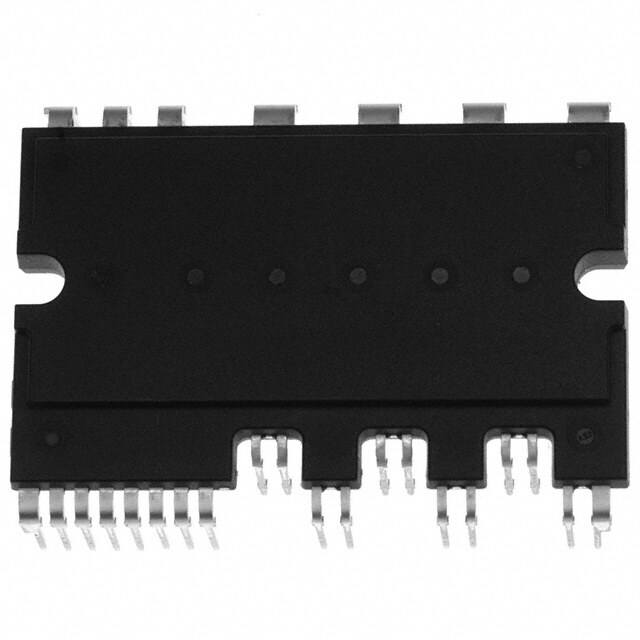
| 封装 | Tube |
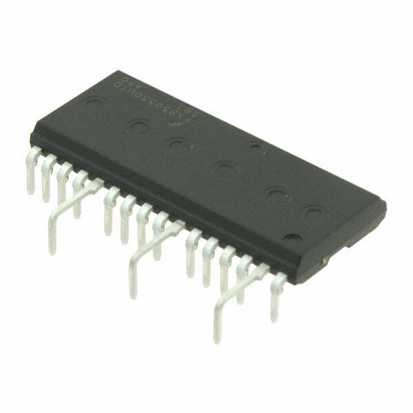
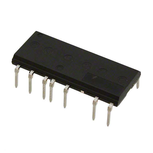
| 封装/外壳 | 26-DIP 模块 |
| 封装/箱体 | SPMAA-C-26 |
| 工作温度 | - 40 C to + 150 C |
| 工作电源电压 | 15 V |
| 工厂包装数量 | 12 |
| 标准包装 | 12 |
| 特色产品 | http://www.digikey.cn/product-highlights/zh/fnc42060f2-motion-spm-45-series/51602 |
| 电压 | 600V |
| 电压-隔离 | 2000Vrms |
| 电流 | 20A |
| 类型 | IGBT |
| 系列 | FNC42060 |
| 输出电流 | 1 mA |
| 配置 | 三相反相器 |


- 商务部:美国ITC正式对集成电路等产品启动337调查
- 曝三星4nm工艺存在良率问题 高通将骁龙8 Gen1或转产台积电
- 太阳诱电将投资9.5亿元在常州建新厂生产MLCC 预计2023年完工
- 英特尔发布欧洲新工厂建设计划 深化IDM 2.0 战略
- 台积电先进制程称霸业界 有大客户加持明年业绩稳了
- 达到5530亿美元!SIA预计今年全球半导体销售额将创下新高
- 英特尔拟将自动驾驶子公司Mobileye上市 估值或超500亿美元
- 三星加码芯片和SET,合并消费电子和移动部门,撤换高东真等 CEO
- 三星电子宣布重大人事变动 还合并消费电子和移动部门
- 海关总署:前11个月进口集成电路产品价值2.52万亿元 增长14.8%
PDF Datasheet 数据手册内容提取
Is Now Part of To learn more about ON Semiconductor, please visit our website at www.onsemi.com Please note: As part of the Fairchild Semiconductor integration, some of the Fairchild orderable part numbers will need to change in order to meet ON Semiconductor’s system requirements. Since the ON Semiconductor product management systems do not have the ability to manage part nomenclature that utilizes an underscore (_), the underscore (_) in the Fairchild part numbers will be changed to a dash (-). This document may contain device numbers with an underscore (_). Please check the ON Semiconductor website to verify the updated device numbers. The most current and up-to-date ordering information can be found at www.onsemi.com. Please email any questions regarding the system integration to Fairchild_questions@onsemi.com. ON Semiconductor and the ON Semiconductor logo are trademarks of Semiconductor Components Industries, LLC dba ON Semiconductor or its subsidiaries in the United States and/or other countries. ON Semiconductor owns the rights to a number of patents, trademarks, copyrights, trade secrets, and other intellectual property. A listing of ON Semiconductor’s product/patent coverage may be accessed at www.onsemi.com/site/pdf/Patent-Marking.pdf. ON Semiconductor reserves the right to make changes without further notice to any products herein. ON Semiconductor makes no warranty, representation or guarantee regarding the suitability of its products for any particular purpose, nor does ON Semiconductor assume any liability arising out of the application or use of any product or circuit, and specifically disclaims any and all liability, including without limitation special, consequential or incidental damages. Buyer is responsible for its products and applications using ON Semiconductor products, including compliance with all laws, regulations and safety requirements or standards, regardless of any support or applications information provided by ON Semiconductor. “Typical” parameters which may be provided in ON Semiconductor data sheets and/or specifications can and do vary in different applications and actual performance may vary over time. All operating parameters, including “Typicals” must be validated for each customer application by customer’s technical experts. ON Semiconductor does not convey any license under its patent rights nor the rights of others. ON Semiconductor products are not designed, intended, or authorized for use as a critical component in life support systems or any FDA Class 3 medical devices or medical devices with a same or similar classification in a foreign jurisdiction or any devices intended for implantation in the human body. Should Buyer purchase or use ON Semiconductor products for any such unintended or unauthorized application, Buyer shall indemnify and hold ON Semiconductor and its officers, employees, subsidiaries, affiliates, and distributors harmless against all claims, costs, damages, and expenses, and reasonable attorney fees arising out of, directly or indirectly, any claim of personal injury or death associated with such unintended or unauthorized use, even if such claim alleges that ON Semiconductor was negligent regarding the design or manufacture of the part. ON Semiconductor is an Equal Opportunity/Affirmative Action Employer. This literature is subject to all applicable copyright laws and is not for resale in any manner.
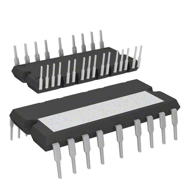
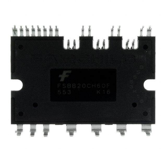
F N C 4 2 January 2014 0 6 FNC42060F / FNC42060F2 0 F / ® F Motion SPM 45 Series N C 4 Features General Description 2 0 6 • UL Certified No. E209204 (UL1557) FNC42060F / FNC42060F2 is an advanced Motion 0 SPM® 45 module providing a fully-featured, high-perfor- F • 600 V - 20 A 3-Phase IGBT Inverter with Integral Gate 2 mance inverter output stage for AC Induction, BLDC, Drivers and Protection and PMSM motors. These modules integrate optimized M o • Low Thermal Resistance Using Ceramic Substrate gate drive of the built-in IGBTs to minimize EMI and t i losses, while also providing multiple on-module protec- o • Low-Loss, Short-Circuit Rated IGBTs n tion features including under-voltage lockouts, over-cur- S • Built-In Bootstrap Diodes and Dedicated Vs Pins Sim- rent shutdown, thermal monitoring, and fault reporting. P plify PCB Layout The built-in, high-speed HVIC requires only a single sup- M ply voltage and translates the incoming logic-level gate ® • Built-In NTC Thermistor for Temperature Monitoring inputs to the high-voltage, high-current drive signals 4 • Separate Open-Emitter Pins from Low-Side IGBTs for required to properly drive the module's robust short-cir- 5 Three-Phase Current Sensing cuit-rated IGBTs. Separate negative IGBT terminals are S e • Single-Grounded Power Supply available for each phase to support the widest variety of ri e control algorithms. s • Optimized for 5 kHz Switching Frequency • Isolation Rating: 2000 V / min. rms Applications • Motion Control - Home Appliance / Industrial Motor Related Resources • AN-9070 - Motion SPM® 45 Series Users Guide • AN-9071 - Motion SPM® 45 Series Thermal Perfor- mance Information • AN-9072 - Motion SPM® 45 Series Mounting Guid- ance • RD-344 - Reference Design (Three Shunt Solution) • RD-345 - Reference Design (One Shunt Solution) Figure 1. Package Overview Package Marking and Ordering Information Device Device Marking Package Packing Type Quantity FNC42060F FNC42060F SPMAA-A26 Rail 12 FNC42060F2 FNC42060F2 SPMAA-C26 Rail 12 ©2013 Fairchild Semiconductor Corporation 1 www.fairchildsemi.com FNC42060F / FNC42060F2 Rev. C3
F N Integrated Power Functions C 4 • 600 V - 20 A IGBT inverter for three-phase DC / AC power conversion (please refer to Figure 3) 2 0 6 Integrated Drive, Protection, and System Control Functions 0 F • For inverter high-side IGBTs: gate drive circuit, high-voltage isolated high-speed level shifting / F control circuit Under-Voltage Lock-Out (UVLO) protection N C • For inverter low-side IGBTs: gate drive circuit, Short-Circuit Protection (SCP) 4 control supply circuit Under-Voltage Lock-Out (UVLO) protection 2 0 • Fault signaling: corresponding to UVLO (low-side supply) and SC faults 6 0 • Input interface: active-HIGH interface, works with 3.3 / 5 V logic, Schmitt trigger input F 2 Pin Configuration M o t i o n S VV ((2266)) P BB((UU)) M VVTTHH((11)) VVSS((UU))((2255)) ® RR ((22)) 4 TTHH VV ((2244)) 5 BB((VV)) S VVSS((VV))((2233)) e r PP((33)) ie VV ((2222)) s BB((WW)) VV ((2211)) SS((WW)) UU((44)) CCaassee TTeemmppeerraattuurree ((TTCC)) IINN((UUHH))((2200)) DDeetteeccttiinngg PPooiinntt IINN ((1199)) ((VVHH)) VV((55)) IINN ((1188)) ((WWHH)) VV ((1177)) CCCC((HH)) VV ((1166)) CCCC((LL)) WW((66)) CCOOMM((1155)) IINN ((1144)) ((UULL)) IINN ((1133)) NN ((77)) ((VVLL)) UU IINN ((1122)) ((WWLL)) NNVV((88)) VVFFOO((1111)) CC ((1100)) NN ((99)) SSCC WW Figure 2. Top View ©2013 Fairchild Semiconductor Corporation 2 www.fairchildsemi.com FNC42060F / FNC42060F2 Rev. C3
F N Pin Descriptions C 4 2 Pin Number Pin Name Pin Description 0 6 1 V Thermistor Bias Voltage 0 TH F 2 RTH Series Resistor for the Use of Thermistor (Temperature Detection) / F 3 P Positive DC-Link Input N 4 U Output for U-Phase C 4 5 V Output for V-Phase 2 0 6 W Output for W-Phase 6 0 7 N Negative DC-Link Input for U-Phase F U 2 8 NV Negative DC-Link Input for V-Phase M 9 N Negative DC-Link Input for W-Phase o W t 10 CSC Capacitor (Low-Pass Filter) for Short-circuit Current Detection Input io n 11 VFO Fault Output S 12 IN Signal Input for Low-Side W-Phase P (WL) M 13 IN(VL) Signal Input for Low-Side V-Phase ® 14 IN(UL) Signal Input for Low-Side U-Phase 4 5 15 COM Common Supply Ground S 16 V Low-Side Common Bias Voltage for IC and IGBTs Driving e CC(L) r i 17 V High-Side Common Bias Voltage for IC and IGBTs Driving e CC(H) s 18 IN(WH) Signal Input for High-Side W-Phase 19 IN Signal Input for High-Side V-Phase (VH) 20 IN Signal Input for High-Side U-Phase (UH) 21 V High-Side Bias Voltage Ground for W-Phase IGBT Driving S(W) 22 V High-Side Bias Voltage for W-Phase IGBT Driving B(W) 23 V High-Side Bias Voltage Ground for V-Phase IGBT Driving S(V) 24 V High-Side Bias Voltage for V-Phase IGBT Driving B(V) 25 V High-Side Bias Voltage Ground for U-Phase IGBT Driving S(U) 26 V High-Side Bias Voltage for U-Phase IGBT Driving B(U) ©2013 Fairchild Semiconductor Corporation 3 www.fairchildsemi.com FNC42060F / FNC42060F2 Rev. C3
F N Internal Equivalent Circuit and Input/Output Pins C 4 2 0 6 0 F VTH (1) / Thermister RTH(2) F N P (3) C (26) VB(U) UVB 4 (25) VS(U) UVS OUT(UH) 20 6 (24) VB(V) VVB UVS U(4) 0 (23) VS(V) VVS F2 (22) VB(W) WVB M (21) VS(W) WVS o OUT(VH) t (20) IN(UH) IN(UH) VVS V (5) ion (19) IN(VH) IN(VH) S (18) IN(WH) IN(WH) P M (17) VCC(H) VCC OUT(WH) ® COM WVS W(6) 4 5 S e (16) VCC(L) VCC r i OUT(UL) e (15) COM s COM (14) IN(UL) IN(UL) NU(7) (13) IN(VL) IN(VL) (12) IN(WL) IN(WL) OUT(VL) (11) VFO VFO NV(8) (10) CSC C(SC) OUT(WL) NW(9) Figure 3. Internal Block Diagram 1st Notes: 1. Inverter high-side is composed of three IGBTs, freewheeling diodes, and one control IC for each IGBT. 2. Inverter low-side is composed of three IGBTs, freewheeling diodes, and one control IC for each IGBT. It has gate drive and protection functions. 3. Inverter power side is composed of four inverter DC-link input terminals and three inverter output terminals. ©2013 Fairchild Semiconductor Corporation 4 www.fairchildsemi.com FNC42060F / FNC42060F2 Rev. C3
F N Absolute Maximum Ratings (T = 25°C, unless otherwise specified.) C J 4 2 Inverter Part 0 6 Symbol Parameter Conditions Rating Unit 0 F VPN Supply Voltage Applied between P - NU, NV, NW 450 V / F VPN(Surge) Supply Voltage (Surge) Applied between P - NU, NV, NW 500 V N C V Collector - Emitter Voltage 600 V CES 4 ± I Each IGBT Collector Current T = 25°C, T <150°C 20 A 2 C C J 0 6 ± ICP Each IGBT Collector Current (Peak) TC = 25°C, TJ < 150°C, Under 1 ms Pulse 40 A 0 Width F 2 PC Collector Dissipation TC = 25°C per Chip 50 W M TJ Operating Junction Temperature (2nd Note 1) -40 ~ 150 °C o t i 2nd Notes: o 1. The maximum junction temperature rating of the power chips integrated within the Motion SPM® 45 product is 150C. n S Control Part P M Symbol Parameter Conditions Rating Unit ® 4 V Control Supply Voltage Applied between V , V - COM 20 V CC CC(H) CC(L) 5 V High - Side Control Bias Voltage Applied between V - V , V - V , 20 V S BS B(U) S(U) B(V) S(V) V - V e B(W) S(W) r i V Input Signal Voltage Applied between IN , IN , IN , -0.3 ~ V + 0.3 V e IN (UH) (VH) (WH) CC s IN(UL), IN(VL), IN(WL) - COM V Fault Output Supply Voltage Applied between V - COM -0.3 ~ V + 0.3 V FO FO CC I Fault Output Current Sink Current at V pin 1 mA FO FO V Current-Sensing Input Voltage Applied between C - COM -0.3 ~ V + 0.3 V SC SC CC Bootstrap Diode Part Symbol Parameter Conditions Rating Unit V Maximum Repetitive Reverse Voltage 600 V RRM I Forward Current T = 25°C, T <150°C 0.50 A F C J I Forward Current (Peak) T = 25°C, T < 150°C, Under 1 ms Pulse 1.50 A FP C J Width T Operating Junction Temperature -40 ~ 150 °C J Total System Symbol Parameter Conditions Rating Unit V Self-Protection Supply Voltage Limit V = V = 13.5 ~ 16.5 V 400 V PN(PROT) CC BS (Short-Circuit Protection Capability) T = 150°C, Non-Repetitive, < 2 s J T Storage Temperature -40 ~ 125 °C STG V Isolation Voltage 60 Hz, Sinusoidal, AC 1 Minute, Connect 2000 V ISO rms Pins to Heat Sink Plate Thermal Resistance Symbol Parameter Conditions Min. Typ. Max. Unit R Junction to Case Thermal Resistance Inverter IGBT Part (per 1 / 6 module) - - 2.5 °C / W th(j-c)Q R Inverter FWDi Part (per 1 / 6 module) - - 3.6 °C / W th(j-c)F 2nd Notes: 2. For the measurement point of case temperature (TC), please refer to Figure 2. ©2013 Fairchild Semiconductor Corporation 5 www.fairchildsemi.com FNC42060F / FNC42060F2 Rev. C3
F N Electrical Characteristics (T = 25°C, unless otherwise specified.) C J 4 2 Inverter Part 0 6 Symbol Parameter Conditions Min. Typ. Max. Unit 0 F VCE(SAT) Collector - Emitter Saturation VCC = VBS = 15 V IC = 20 A, TJ = 25°C - 1.85 2.35 V / Voltage V = 5 V F IN N V FWDi Forward Voltage V = 0 V I = 20 A, T = 25°C - 1.95 2.45 V C F IN F J 4 HS tON Switching Times VPN = 300 V, VCC = VBS = 15 V, IC = 20 A 0.45 0.75 1.25 s 2 T = 25°C 0 t J - 0.20 0.45 s 6 C(ON) VIN = 0 V 5 V, Inductive Load 0 tOFF (2nd Note 3) - 0.70 1.20 s F 2 tC(OFF) - 0.15 0.40 s M trr - 0.15 - s o t LS tON VPN = 300 V, VCC = VBS = 15 V, IC = 20 A 0.45 0.75 1.25 s io T = 25°C n t J - 0.20 0.45 s C(ON) VIN = 0 V 5 V, Inductive Load S tOFF (2nd Note 3) - 0.75 1.25 s P M t - 0.15 0.40 s C(OFF) ® trr - 0.15 - s 4 5 ICES Collector - Emitter Leakage VCE = VCES - - 5 mA S Current e r 2nd Notes: ie 3. tthOeN daentda ilteOdF Fin ifnocrlmudaeti othne, pplreoapsaeg saetieo nF idgeulraey 4o.f the internal drive IC. tC(ON) and tC(OFF) are the switching time of IGBT itself under the given gate driving condition internally. For s 100% IC 100% IC t rr V I I V CE C C CE VIN VIN t ON t OFF t t C(ON) C(OFF) 10% IC VIN(ON) 90% IC 10% VCE VIN(OFF) 10% VCE 10% IC (a) turn-on (b) turn-off Figure 4. Switching Time Definition ©2013 Fairchild Semiconductor Corporation 6 www.fairchildsemi.com FNC42060F / FNC42060F2 Rev. C3
F N C 4 2 0 6 0 F / F N C 4 2 0 6 0 F 2 M o t i o n S P M ® Figure 5. Switching Loss Characteristics (Typical) 4 5 S Control Part e r i Symbol Parameter Conditions Min. Typ. Max. Unit e s IQCCH Quiescent VCC Supply VCC(H) = 15 V, IN(UH,VH,WH) = 0 V VCC(H) - COM - - 0.10 mA Current I V = 15 V, IN = 0 V V - COM - - 2.65 mA QCCL CC(L) (UL,VL, WL) CC(L) I Operating V Supply V = 15 V, f = 20 kHz, duty V - COM - - 0.15 mA PCCH CC CC(L) PWM CC(H) Current = 50%, Applied to One PWM Sig- nal Input for High-Side I V = 15 V, f = 20 kHz, duty V - COM - - 4.00 mA PCCL CC(L) PWM CC(L) = 50%, Applied to One PWM Sig- nal Input for Low-Side I Quiescent V Supply V = 15 V, IN = 0 V V - V , V - - - 0.30 mA QBS BS BS (UH, VH, WH) B(U) S(U) B(V) Current V , V - V S(V) B(W) S(W) I Operating V Supply V = V = 15 V, f = 20 kHz, V - V , V - - - 2.00 mA PBS BS CC BS PWM B(U) S(U) B(V) Current Duty = 50%, Applied to One PWM V , V - V S(V) B(W) S(W) Signal Input for High-Side V Fault Output Voltage V = 0 V, V Circuit: 10 k to 5 V Pull-up 4.5 - - V FOH SC FO V V = 1 V, V Circuit: 10 k to 5 V Pull-up - - 0.5 V FOL SC FO V Short-Circuit V = 15 V (2nd Note 4) 0.45 0.50 0.55 V SC(ref) CC Current Trip Level UV Detection level 10.5 - 13.0 V CCD Supply Circuit UV Reset level 11.0 - 13.5 V CCR Under-Voltage UVBSD Protection Detection level 10.0 - 12.5 V UV Reset level 10.5 - 13.0 V BSR t Fault-Out Pulse Width 30 - - s FOD V ON Threshold Voltage Applied between IN , IN , IN , IN , IN , - - 2.6 V IN(ON) (UH) (VH) (WH) (UL) (VL) IN - COM V OFF Threshold Voltage (WL) 0.8 - - V IN(OFF) R Resistance of @T = 25°C, (2nd Note 5) - 47 - k TH TH Thermister @T = 100°C - 2.9 - k TH 2nd Notes: 4. Short-circuit protection is functioning only at the low-sides. 5. TTH is the temperature of thermister itselt. To know case temperature (TC), please make the experiment considering your application. ©2013 Fairchild Semiconductor Corporation 7 www.fairchildsemi.com FNC42060F / FNC42060F2 Rev. C3
F N C 4 R-T C urve 2 0 600 6 0 550 F R-T Curve in 50℃ ~ 125℃ 500 20 / F N 450 16 C ] 4 ance[k] 334050000 esistance[k 128 2060F2 st 250 R 4 si M Re 200 0 o 50 60 70 80 90 100 110 120 t i 150 Tempera ture [℃] o n 100 S P 50 M 0 ® -20 -10 0 10 20 30 40 50 60 70 80 90 100 110 120 4 5 Temperature T [℃] TH S e r Figure. 6. R-T Curve of The Built-In Thermistor ie s Bootstrap Diode Part Symbol Parameter Conditions Min. Typ. Max. Unit V Forward Voltage I = 0.1 A, T = 25°C - 2.5 - V F F C t Reverse-Recovery Time I = 0.1 A, T = 25°C - 80 - ns rr F C Built-In Bootstrap Diod e V -I Characteristic F F 1.0 0.9 0.8 0.7 0.6 A] 0.5 I [F 0.4 0.3 0.2 0.1 T=25oC C 0.0 0 1 2 3 4 5 6 7 8 9 10 11 12 13 14 15 V [V] F Figure 7. Built-In Bootstrap Diode Characteristic 2nd Notes: 6. Built-in bootstrap diode includes around 15 Ω resistance characteristic. ©2013 Fairchild Semiconductor Corporation 8 www.fairchildsemi.com FNC42060F / FNC42060F2 Rev. C3
F N Recommended Operating Conditions C 4 2 Symbol Parameter Conditions Min. Typ. Max. Unit 0 6 V Supply Voltage Applied between P - N , N , N - 300 400 V 0 PN U V W F VCC Control Supply Voltage Applied between VCC(H), VCC(L) - COM 13.5 15.0 16.5 V / F VBS High-Side Bias Voltage Applied between VB(U) - VS(U), VB(V) - VS(V), VB(W) - 13.0 15.0 18.5 V N VS(W) C 4 dVCC / dt, Control Supply Variation -1 - 1 V / s 2 dV / dt 0 BS 6 t Blanking Time for For each input signal 1.5 - - s 0 dead F Preventing Arm-Short 2 fPWM PWM Input Signal - 40C <TJ <150°C - - 20 kHz M V Voltage for Current Applied between N , N , N - COM -4 4 V o SEN U V W t Sensing (Including Surge-Voltage) io n P Minimun Input Pulse (2nd Note 7) 0.7 - - s WIN(ON) S Width PWIN(OFF) 0.7 - - P M ® 2nd Notes: 4 7. This product might not make response if input pulse width is less than the recommanded value. 5 S e r i e s Figure 8. Allowable Maximum Output Current 2nd Notes: 8. This allowable output current value is the reference data for the safe operation of this product. This may be different from the actual application and operating condition. ©2013 Fairchild Semiconductor Corporation 9 www.fairchildsemi.com FNC42060F / FNC42060F2 Rev. C3
F N Mechanical Characteristics and Ratings C 4 2 Parameter Conditions Min. Typ. Max. Unit 0 6 Device Flatness See Figure 9 0 - + 120 m 0 F Mounting Torque Mounting Screw: M3 Recommended 0.7 N • m 0.6 0.7 0.8 N • m / F See Figure 10 Recommended 7.1 kg • cm 6.2 7.1 8.1 kg • cm N C Weight - 11.00 - g 4 2 0 6 0 F 2 M o t i o n S P M ® 4 5 S e r i e s Figure 9. Flatness Measurement Position PPrree -- SSccrreewwiinngg :: 11→→22 22 FFiinnaall SSccrreewwiinngg :: 22→→11 11 Figure 10. Mounting Screws Torque Order 2nd Notes: 9. Do not make over torque when mounting screws. Much mounting torque may cause ceramic cracks, as well as bolts and Al heat-sink destruction. 10. Avoid one side tightening stress. Figure 10 shows the recommended torque order for mounting screws. Uneven mounting can cause the ceramic substrate of the SPM® 45 package to be damaged. The pre-screwing torque is set to 20 ~ 30% of maximum torque rating. ©2013 Fairchild Semiconductor Corporation 10 www.fairchildsemi.com FNC42060F / FNC42060F2 Rev. C3
F N Time Charts of Protective Function C 4 2 0 6 0 F Input Signal / F N Protection C RESET SET RESET 4 Circuit State 2 0 UV 6 CCR 0 Control a1 UV a6 F CCD a3 2 Supply Voltage M a2 a4 a7 o t i o n Output Current S P M a5 Fault Output Signal ® 4 5 a1 : Control supply voltage rises: after the voltage rises UV , the circuits start to operate when next input is applied. S CCR e a2 : Normal operation: IGBT ON and carrying current. r i e a3 : Under-voltage detection (UVCCD). s a4 : IGBT OFF in spite of control input condition. a5 : Fault output operation starts. a6 : Under-voltage reset (UV ). CCR a7 : Normal operation: IGBT ON and carrying current. Figure 11. Under-Voltage Protection (Low-Side) Input Signal Protection RESET SET RESET Circuit State UV BSR b1 b5 Control UV BSD b3 Supply Voltage b6 b2 b4 Output Current High-level (no fault output) Fault Output Signal b1 : Control supply voltage rises: after the voltage reaches UV , the circuits start to operate when next input is applied. BSR b2 : Normal operation: IGBT ON and carrying current. b3 : Under-voltage detection (UV ). BSD b4 : IGBT OFF in spite of control input condition, but there is no fault output signal. b5 : Under-voltage reset (UV ). BSR b6 : Normal operation: IGBT ON and carrying current. Figure 12. Under-Voltage Protection (High-Side) ©2013 Fairchild Semiconductor Corporation 11 www.fairchildsemi.com FNC42060F / FNC42060F2 Rev. C3
F N C 4 2 Lower Arms 0 c6 c7 6 Control Input 0 F Protection / Circuit State SET RESET F N C Internal IGBT 4 c4 2 Gate - Emitter Voltage c3 0 c2 6 0 SC F 2 c1 M Output Current c8 o t i o n SC Reference Voltage S Sensing Voltage P of Shunt Resistance M ® 4 CR Circuit Time 5 Fault Output Signal c5 Constant Delay S e r i e (with the external shunt resistance and CR connection) s c1 : Normal operation: IGBT ON and carrying current. c2 : Short-circuit current detection (SC trigger). c3 : Hard IGBT gate interrupt. c4 : IGBT turns OFF. c5 : Input “LOW”: IGBT OFF state. c6 : Input “HIGH”: IGBT ON state, but during the active period of fault output, the IGBT doesn’t turn ON. c7 : IGBT OFF state. Figure 13. Short-Circuit Protection (Low-Side Operation Only) Input/Output Interface Circuit +5 V (for MCU or Control power) R = 10 kΩ SPM PF IN , IN , IN (UH) (VH) (WH) IN , IN , IN (UL) (VL) (WL) MCU V FO COM Figure 14. Recommended MCU I/O Interface Circuit 2nd Notes: 11. RC coupling at each input (parts shown dotted) might change depending on the PWM control scheme in the application and the wiring impedance of the application’s printed circuit board. The input signal section of the Motion SPM® 45 product integrates a 5 k(typ.) pull-down resistor. Therefore, when using an external filtering resistor, pay atten- tion to the signal voltage drop at input terminal. ©2013 Fairchild Semiconductor Corporation 12 www.fairchildsemi.com FNC42060F / FNC42060F2 Rev. C3
F N C 4 2 0 6 0 HVIC (26) VB(U) VB(U) P (3) F CBS CBSC (25) VS(U) VS(U) / F Gating UH RS (20) IN(UH) IN(UH) OUVT(SU(UH)) U (4) NC (24) VB(V) VB(V) 4 2 Gating VH RS CBS CBSC ((1293)) IVNS((VVH)) IVNS(V(VH)) OUT(VH) 060 (22) VB(W) VB(W) VS(V) V (5) M F2 CBS CBSC (21) VS(W) VS(W) M M Gating WH RS +15 V ((1187)) IVNC(CW(HH)) IVNC(WCH) OUT(WH) CDCS VDC oti C CPS CPS CPS CSP15 CSPC15 (15) COM COM VS(W) W (6) on U S +5 V LVIC P (16) VCC(L) VCC M Fault RSRPF CSPC05 CSP05 (11) VFO VFO OUT(UL) NU(7) RSU ® 45 CBPF CPF OUT(VL) S GGGaaatttiiinnnggg WVULLL RRRSSS (((111432))) IIINNN(((UVWLLL))) IIINNN(((WVULLL))) NV(8) RSV eries CSC COM OUT(WL) CPS CPS CPS RF ((11)0 )V CTHSC CSC NW(9) RSW RTH (2) RTH THERMISTOR U-Phase Current Input Signal for V-Phase Current Short-Circuit Protection Temp. Monitoring W-Phase Current Figure 15. Typical Application Circuit 3rd Notes: 1) To avoid malfunction, the wiring of each input should be as short as possible (less than 2 - 3 cm). 2) By virtue of integrating an application-specific type of HVIC inside the Motion SPM® 45 product, direct coupling to MCU terminals without any optocoupler or transformer isola- tion is possible. 3) VFO output is open-drain type. This signal line should be pulled up to the positive side of the MCU or control power supply with a resistor that makes IFO up to 1 mA (please refer to Figure 14). 4) CSP15 of around seven times larger than bootstrap capacitor CBS is recommended. 5) Input signal is active-HIGH type. There is a 5 k resistor inside the IC to pull down each input signal line to GND. RC coupling circuits is recommanded for the prevention of input signal oscillation. RSCPS time constant should be selected in the range 50 ~ 150 ns (recommended RS = 100 Ω, CPS = 1 nF). 6) To prevent errors of the protection function, the wiring around RF and CSC should be as short as possible. 7) In the short-circuit protection circuit, please select the RFCSC time constant in the range 1.5 ~ 2 s. 8) The connection between control GND line and power GND line which includes the NU, NV, NW must be connected to only one point. Please do not connect the control GND to the power GND by the broad pattern. Also, the wiring distance between control GND and power GND should be as short as possible. 9) Each capacitor should be mounted as close to the pins of the Motion SPM 45 product as possible. 10) To prevent surge destruction, the wiring between the smoothing capacitor and the P & GND pins should be as short as possible. The use of a high-frequency non-inductive capacitor of around 0.1 ~ 0.22 F between the P and GND pins is recommended. 11) Relays are used in almost every systems of electrical equipment in home appliances. In these cases, there should be sufficient distance between the MCU and the relays. 12) The zener diode or transient voltage suppressor should be adopted for the protection of ICs from the surge destruction between each pair of control supply terminals (recommanded zener diode is 22 V / 1 W, which has the lower zener impedance characteristic than about 15 Ω). 13) Please choose the electrolytic capacitor with good temperature characteristic in CBS. Also, choose 0.1 ~ 0.2 F R-category ceramic capacitors with good temperature and frequency characteristics in CBSC. 14) For the detailed information, please refer to the AN-9070, AN-9071, AN-9072, RD-344, and RD-345. ©2013 Fairchild Semiconductor Corporation 13 www.fairchildsemi.com FNC42060F / FNC42060F2 Rev. C3
F N Detailed Package Outline Drawings (FNC42060F) C 4 2 0 6 0 F / F N C 4 2 0 6 0 F 2 M o t i o n S P M ® 4 5 S e r i e s Package drawings are provided as a service to customers considering Fairchild components. Drawings may change in any manner without notice. Please note the revision and/or data on the drawing and contact a FairchildSemiconductor representative to verify or obtain the most recent revision. Package specifications do not expand the terms of Fairchild’s worldwide therm and conditions, specifically the the warranty therein, which covers Fairchild products. Always visit Fairchild Semiconductor’s online packaging area for the most recent package drawings: http://www.fairchildsemi.com/dwg/MO/MOD26AA.pdf ©2013 Fairchild Semiconductor Corporation 14 www.fairchildsemi.com FNC42060F / FNC42060F2 Rev. C3
F N Detailed Package Outline Drawings (FNC42060F2, Long Terminal Type) C 4 2 0 6 0 F / F N C 4 2 0 6 0 F 2 M o t i o n S P M ® 4 5 S e r i e s Package drawings are provided as a service to customers considering Fairchild components. Drawings may change in any manner without notice. Please note the revision and/or data on the drawing and contact a FairchildSemiconductor representative to verify or obtain the most recent revision. Package specifications do not expand the terms of Fairchild’s worldwide therm and conditions, specifically the the warranty therein, which covers Fairchild products. Always visit Fairchild Semiconductor’s online packaging area for the most recent package drawings: http://www.fairchildsemi.com/dwg/MO/MOD26AC.pdf ©2013 Fairchild Semiconductor Corporation 15 www.fairchildsemi.com FNC42060F / FNC42060F2 Rev. C3
©2013 Fairchild Semiconductor Corporation 16 www.fairchildsemi.com FNC42060F / FNC42060F2 Rev. C3
ON Semiconductor and are trademarks of Semiconductor Components Industries, LLC dba ON Semiconductor or its subsidiaries in the United States and/or other countries. ON Semiconductor owns the rights to a number of patents, trademarks, copyrights, trade secrets, and other intellectual property. A listing of ON Semiconductor’s product/patent coverage may be accessed at www.onsemi.com/site/pdf/Patent−Marking.pdf. ON Semiconductor reserves the right to make changes without further notice to any products herein. ON Semiconductor makes no warranty, representation or guarantee regarding the suitability of its products for any particular purpose, nor does ON Semiconductor assume any liability arising out of the application or use of any product or circuit, and specifically disclaims any and all liability, including without limitation special, consequential or incidental damages. Buyer is responsible for its products and applications using ON Semiconductor products, including compliance with all laws, regulations and safety requirements or standards, regardless of any support or applications information provided by ON Semiconductor. “Typical” parameters which may be provided in ON Semiconductor data sheets and/or specifications can and do vary in different applications and actual performance may vary over time. All operating parameters, including “Typicals” must be validated for each customer application by customer’s technical experts. ON Semiconductor does not convey any license under its patent rights nor the rights of others. ON Semiconductor products are not designed, intended, or authorized for use as a critical component in life support systems or any FDA Class 3 medical devices or medical devices with a same or similar classification in a foreign jurisdiction or any devices intended for implantation in the human body. Should Buyer purchase or use ON Semiconductor products for any such unintended or unauthorized application, Buyer shall indemnify and hold ON Semiconductor and its officers, employees, subsidiaries, affiliates, and distributors harmless against all claims, costs, damages, and expenses, and reasonable attorney fees arising out of, directly or indirectly, any claim of personal injury or death associated with such unintended or unauthorized use, even if such claim alleges that ON Semiconductor was negligent regarding the design or manufacture of the part. ON Semiconductor is an Equal Opportunity/Affirmative Action Employer. This literature is subject to all applicable copyright laws and is not for resale in any manner. PUBLICATION ORDERING INFORMATION LITERATURE FULFILLMENT: N. American Technical Support: 800−282−9855 Toll Free ON Semiconductor Website: www.onsemi.com Literature Distribution Center for ON Semiconductor USA/Canada 19521 E. 32nd Pkwy, Aurora, Colorado 80011 USA Europe, Middle East and Africa Technical Support: Order Literature: http://www.onsemi.com/orderlit Phone: 303−675−2175 or 800−344−3860 Toll Free USA/Canada Phone: 421 33 790 2910 Fax: 303−675−2176 or 800−344−3867 Toll Free USA/Canada Japan Customer Focus Center For additional information, please contact your local Email: orderlit@onsemi.com Phone: 81−3−5817−1050 Sales Representative © Semiconductor Components Industries, LLC www.onsemi.com www.onsemi.com 1
Mouser Electronics Authorized Distributor Click to View Pricing, Inventory, Delivery & Lifecycle Information: O N Semiconductor: FNC42060F2