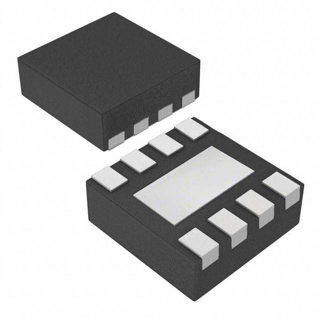
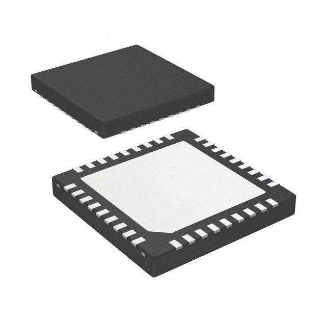
ICGOO在线商城 > 集成电路(IC) > 接口 - 信号缓冲器,中继器,分配器 > FIN1104MTCX
- 型号: FIN1104MTCX
- 制造商: Fairchild Semiconductor
- 库位|库存: xxxx|xxxx
- 要求:
| 数量阶梯 | 香港交货 | 国内含税 |
| +xxxx | $xxxx | ¥xxxx |
查看当月历史价格
查看今年历史价格
FIN1104MTCX产品简介:
ICGOO电子元器件商城为您提供FIN1104MTCX由Fairchild Semiconductor设计生产,在icgoo商城现货销售,并且可以通过原厂、代理商等渠道进行代购。 FIN1104MTCX价格参考¥4.62-¥12.27。Fairchild SemiconductorFIN1104MTCX封装/规格:接口 - 信号缓冲器,中继器,分配器, Buffer, ReDriver 4 Channel 800Mbps 24-TSSOP。您可以下载FIN1104MTCX参考资料、Datasheet数据手册功能说明书,资料中有FIN1104MTCX 详细功能的应用电路图电压和使用方法及教程。
| 参数 | 数值 |
| 产品目录 | 集成电路 (IC)半导体 |
| 描述 | IC REPEATER 4 PORT LVDS 24TSSOP缓冲器和线路驱动器 4 Port Repeater LVDS Hi Speed |
| 产品分类 | |
| 品牌 | Fairchild Semiconductor |
| 产品手册 | |
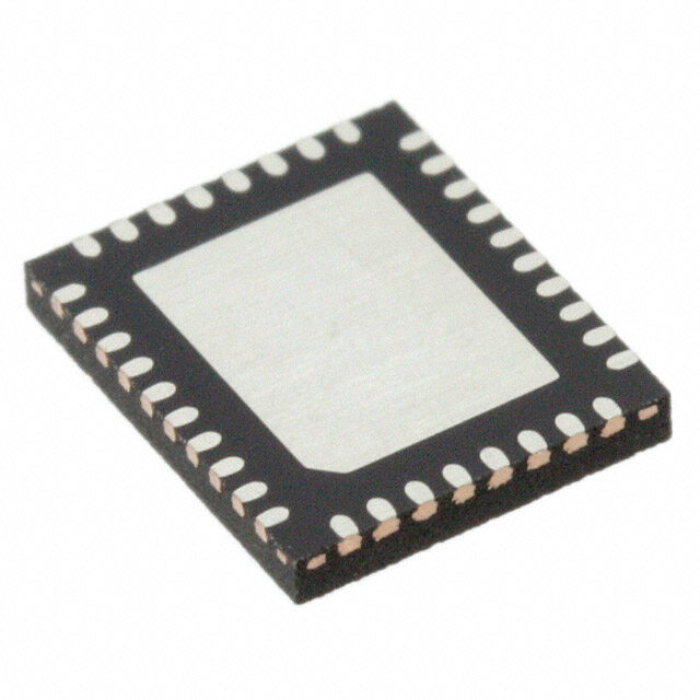
| 产品图片 |
|
| rohs | 符合RoHS无铅 / 符合限制有害物质指令(RoHS)规范要求 |
| 产品系列 | 逻辑集成电路,缓冲器和线路驱动器,Fairchild Semiconductor FIN1104MTCX- |
| 数据手册 | |
| 产品型号 | FIN1104MTCX |
| Tx/Rx类型 | LVDS |
| 产品种类 | 缓冲器和线路驱动器 |
| 供应商器件封装 | 24-TSSOP |
| 其它名称 | FIN1104MTCXDKR |
| 包装 | Digi-Reel® |
| 单位重量 | 212 mg |
| 商标 | Fairchild Semiconductor |
| 安装类型 | 表面贴装 |
| 安装风格 | SMD/SMT |
| 封装 | Reel |
| 封装/外壳 | 24-TSSOP(0.173",4.40mm 宽) |
| 封装/箱体 | TSSOP-24 |
| 工作温度 | -40°C ~ 85°C |
| 工厂包装数量 | 2500 |
| 应用 | LVDS |
| 延迟时间 | 1.75ns |
| 接口 | EIA/TIA-644-A |
| 数据速率 | 800 Mbps |
| 数据速率(最大值) | 800Mbps |
| 最大工作温度 | + 150 C |
| 最小工作温度 | - 65 C |
| 标准包装 | 1 |
| 电压-电源 | 3 V ~ 3.6 V |
| 电容-输入 | 2.6pF |
| 电流-电源 | 41mA |
| 电源电压-最大 | 3.6 V |
| 电源电压-最小 | 3 V |
| 电源电流 | 11 mA |
| 类型 | 缓冲器, 转接驱动器 |
| 系列 | FIN1104 |
| 输入 | LVDS,LVPECL |
| 输出 | LVDS |
| 通道数 | 4 |




- 商务部:美国ITC正式对集成电路等产品启动337调查
- 曝三星4nm工艺存在良率问题 高通将骁龙8 Gen1或转产台积电
- 太阳诱电将投资9.5亿元在常州建新厂生产MLCC 预计2023年完工
- 英特尔发布欧洲新工厂建设计划 深化IDM 2.0 战略
- 台积电先进制程称霸业界 有大客户加持明年业绩稳了
- 达到5530亿美元!SIA预计今年全球半导体销售额将创下新高
- 英特尔拟将自动驾驶子公司Mobileye上市 估值或超500亿美元
- 三星加码芯片和SET,合并消费电子和移动部门,撤换高东真等 CEO
- 三星电子宣布重大人事变动 还合并消费电子和移动部门
- 海关总署:前11个月进口集成电路产品价值2.52万亿元 增长14.8%


PDF Datasheet 数据手册内容提取
Is Now Part of To learn more about ON Semiconductor, please visit our website at www.onsemi.com Please note: As part of the Fairchild Semiconductor integration, some of the Fairchild orderable part numbers will need to change in order to meet ON Semiconductor’s system requirements. Since the ON Semiconductor product management systems do not have the ability to manage part nomenclature that utilizes an underscore (_), the underscore (_) in the Fairchild part numbers will be changed to a dash (-). This document may contain device numbers with an underscore (_). Please check the ON Semiconductor website to verify the updated device numbers. The most current and up-to-date ordering information can be found at www.onsemi.com. Please email any questions regarding the system integration to Fairchild_questions@onsemi.com. ON Semiconductor and the ON Semiconductor logo are trademarks of Semiconductor Components Industries, LLC dba ON Semiconductor or its subsidiaries in the United States and/or other countries. ON Semiconductor owns the rights to a number of patents, trademarks, copyrights, trade secrets, and other intellectual property. A listing of ON Semiconductor’s product/patent coverage may be accessed at www.onsemi.com/site/pdf/Patent-Marking.pdf. ON Semiconductor reserves the right to make changes without further notice to any products herein. ON Semiconductor makes no warranty, representation or guarantee regarding the suitability of its products for any particular purpose, nor does ON Semiconductor assume any liability arising out of the application or use of any product or circuit, and specifically disclaims any and all liability, including without limitation special, consequential or incidental damages. Buyer is responsible for its products and applications using ON Semiconductor products, including compliance with all laws, regulations and safety requirements or standards, regardless of any support or applications information provided by ON Semiconductor. “Typical” parameters which may be provided in ON Semiconductor data sheets and/or specifications can and do vary in different applications and actual performance may vary over time. All operating parameters, including “Typicals” must be validated for each customer application by customer’s technical experts. ON Semiconductor does not convey any license under its patent rights nor the rights of others. ON Semiconductor products are not designed, intended, or authorized for use as a critical component in life support systems or any FDA Class 3 medical devices or medical devices with a same or similar classification in a foreign jurisdiction or any devices intended for implantation in the human body. Should Buyer purchase or use ON Semiconductor products for any such unintended or unauthorized application, Buyer shall indemnify and hold ON Semiconductor and its officers, employees, subsidiaries, affiliates, and distributors harmless against all claims, costs, damages, and expenses, and reasonable attorney fees arising out of, directly or indirectly, any claim of personal injury or death associated with such unintended or unauthorized use, even if such claim alleges that ON Semiconductor was negligent regarding the design or manufacture of the part. ON Semiconductor is an Equal Opportunity/Affirmative Action Employer. This literature is subject to all applicable copyright laws and is not for resale in any manner.
F January 2002 IN Revised January 2003 1 1 0 4 L FIN1104 V D S LVDS 4 Port High Speed Repeater 4 P General Description Features o r t This 4 port repeater is designed for high speed intercon- (cid:1) Greater than 800 Mbps data rate H nects utilizing Low Voltage Differential Signaling (LVDS) (cid:1) 3.3V power supply operation ig technology. The FIN1104 accepts and outputs LVDS levels (cid:1) 3.5 ps maximum random jitter and 135 ps maximum h with a typical differential output swing of 330 mV which pro- deterministic jitter S vides low EMI at ultra low power dissipation even at high p fcroeuqpuleinngc ioens .t hTeh ein FpIuNts1.1 I0n4 a pdrdoivtiiodne sth ae VFBINB 1r1ef0e4r ecnacne d fiorer cAtlCy (cid:1)(cid:1) WLViDdeS rarile-tcoe-irvaeilr coinmpmutosn macocdeep tr anLVgePECL, HSTL, and eed accept LVPECL, HSTL, and SSTL-2 for translation to SSTL-2 directly R LVDS. (cid:1) Ultra low power consumption e (cid:1) 20 ps typical channel-to-channel skew p e (cid:1) Power off protection a (cid:1) > 7.5 kV HBM ESD Protection te r (cid:1) Meets or exceeds the TIA/EIA-644-A LVDS standard (cid:1) Available in space saving 24-Lead TSSOP package (cid:1) Open circuit fail safe protection (cid:1) VBB reference output Ordering Code: Order Number Package Number Package Description FIN1104MTC MTC24 24-Lead Thin Shrink Small Outline Package (TSSOP), JEDEC MO-153, 4.4mm Wide Devices also available in Tape and Reel. Specify by appending suffix letter “X” to the ordering code. Pin Descriptions Connection Diagram Pin Name Description RIN1+, RIN2+, Non-inverting LVDS Input RIN3+, RIN4+ RIN1−, RIN2−, Inverting LVDS Input RIN3−, RIN4− DOUT1+, DOUT2+, Non-inverting Driver Output DOUT3+, DOUT4+ DOUT1−, DOUT2−, Inverting Driver Output DOUT3−, DOUT4− EN Driver Enable Pin for All Output EN Inverting Driver Enable Pin for all Outputs VCC Power Supply GND Ground VBB Reference Voltage Output © 2003 Fairchild Semiconductor Corporation DS500656 www.fairchildsemi.com
4 0 Function Table Functional Diagram 1 1 N Inputs Outputs I F EN EN DIN+ DIN− DOUT+ DOUT− H L H L H L H L L H L H H L Fail Safe Case H L X H X X Z Z L X X X Z Z H = HIGH Logic Level L = LOW Logic Level X = Don’t Care Z = High Impedance www.fairchildsemi.com 2
F Absolute Maximum Ratings(Note 1) Recommended Operating IN Conditions 1 Supply Voltage (VCC) −0.5V to +4.6V 10 LVDS DC Input Voltage (VIN) −0.5V to +4.6V Supply Voltage (VCC) 3.0V to 3.6V 4 LVDS DC Output Voltage (VOUT) −0.5V to +4.6V Magnitude of Differential Driver Short Circuit Current (IOSD) Continuous 10 mA Voltage (|VID|) 100 mV to VCC Storage Temperature Range (TSTG) −65°C to +150°C Common Mode Voltage Max Junction Temperature (TJ) 150°C Range (VIC) (0V + |VID|/2) to (VCC − |VID|/2) Lead Temperature (TL) Operating Temperature (TA) −40°C to +85°C (Soldering, 10 seconds) 260°C ESD (Human Body Model) 7500V Note 1: The “Absolute Maximum Ratings”: are those values beyond which ESD (Machine Model) 400V damage to the device may occur. The databook specifications should be met, without exception, to ensure that the system design is reliable over its power supply, temperature and output/input loading variables. Fairchild does not recommend operation of circuits outside databook specification. DC Electrical Characteristics Min Typ Max Symbol Parameter Test Conditions Units (Note 2) VTH Differential Input Threshold HIGH See Figure 1; VIC = +0.05V, +1.2V, or VCC − 0.05V 100 mV VTL Differential Input Threshold LOW See Figure 1; VIC = +0.05V, +1.2V, or VCC − 0.05V −100 mV VIH Input HIGH Voltage (EN or EN) 2.0 VCC V VIL Input LOW Voltage (EN or EN) GND 0.8 V VOD Output Differential Voltage 250 330 450 mV ∆VOD VOD Magnitude Change from 25 mV Differential LOW-to-HIGH RL = 100 Ω, Driver Enabled, VOS Offset Voltage See Figure 2 1.125 1.23 1.375 V ∆VOS Offset Magnitude Change from 25 mV Differential LOW-to-HIGH IOS Short Circuit Output Current DOUT+ = 0V and DOUT− = 0V, −3.4 −6 mA Driver Enabled VOD = 0V, Driver Enabled ±3.4 ±6 mA IIN Input Current (EN, EN, DINx+, DINx−) VIN = 0V to VCC, Other Input = VCC or 0V ±20 µA (for Differential Inputs) IOFF Power Off Input or Output Current VCC = 0V, VIN or VOUT = 0V to 3.6V ±20 µA ICCZ Disabled Power Supply Current Drivers Disabled 5.4 11 mA ICC Power Supply Current Drivers Enabled, Any Valid Input Condition 30.4 41 mA IOZ Disabled Output Leakage Current Driver Disabled, DOUT+ = 0V to 3.6V or ±20 µA DOUT− = 0V to3.6V VIC Common Mode Voltage Range |VID| = 100 mV to VCC 0V + |VID|/2 VCC − (|VID|/2) V CIN Input Capacitance Enable Input 2.6 pF LVDS Input 2.1 COUT Output Capacitance 2.8 pF VBB Output Reference Voltage VCC = 3.3V, IBB = 0 to −275 µA 1.125 1.2 1.375 V Note 2: All typical values are at TA = 25°C and with VCC = 3.3V. 3 www.fairchildsemi.com
4 0 AC Electrical Characteristics 1 1 N Over supply voltage and operating temperature ranges, unless otherwise specified I F Min Typ Max Symbol Parameter Test Conditions Units (Note 3) tPLHD Differential Output Propagation Delay 0.75 1.1 1.75 ns LOW-to-HIGH tPHLD Differential Output Propagation Delay 0.75 1.1 1.75 ns HIGH-to-LOW RL = 100 Ω, CL = 5 pF, tTLHD Differential Output Rise Time (20% to 80%) VID = 200 mV to 450 mV, 0.29 0.4 0.58 ns tTHLD Differential Output Fall Time (80% to 20%) VIC = |VID|/2 to VCC − (|VID|/2), 0.29 0.4 0.58 ns tSK(P) Pulse Skew |tPLH - tPHL| Duty Cycle = 50%, 0.02 0.2 ns tSK(LH), Channel-to-Channel Skew See Figure 1 and Figure 3 0.02 0.15 ns tSK(HL) (Note 4) 0.02 tSK(PP) Part-to-Part Skew (Note 5) 0.5 ns fMAX Maximum Frequency (Note 6)(Note 7) 400 800 MHz tPZHD Differential Output Enable Time 2.2 5 ns from Z to HIGH tPZLD Differential Output Enable Time 2.5 5 ns from Z to LOW RL = 100 Ω, CL = 5 pF, tPHZD Differential Output Disable Time See Figure 2 and Figure 3 1.8 5 ns from HIGH to Z tPLZD Differential Output Disable Time 2.1 5 ns from LOW to Z tDJ LVDS Data Jitter, VID = 300 mV, PRBS = 223 - 1, 85 135 ps Deterministic VIC = 1.2V at 800 Mbps tRJ LVDS Clock Jitter, VID = 300 mV, 2.1 3.5 ps Random (RMS) VIC = 1.2V at 400 MHz Note 3: All typical values are at TA = 25°C and with VCC = 3.3V. Note 4: tSK(LH), tSK(HL) is the skew between specified outputs of a single device when the outputs have identical loads and are switching in the same direc- tion. Note 5: tSK(PP) is the magnitude of the difference in propagation delay times between any specified terminals of two devices switching in the same direction (either Low-to-HIGH or HIGH-to-LOW) when both devices operate with the same supply voltage, same temperature, and have identical test circuits. Note 6: Passing criteria for maximum frequency is the output VOD > 200 mV and the duty cycle is 45% to 55% with all channels switching. Note 7: Output loading is transmission line environment only; CL is < 1 pF of stray test fixture capacitance. FIGURE 1. Differential Receiver Voltage Definitions and Propagation and Transition Time Test Circuit Note A: All LVDS input pulses have frequency = 10 MHz, tR or tF < = 0.5 ns Note B: CL includes all probe and test fixture capacitances FIGURE 3. Differential Driver Propagation Delay and Transition Time Test Circuit FIGURE 2. Differential Driver DC Test Circuit www.fairchildsemi.com 4
F IN 1 1 0 4 FIGURE 4. AC Waveform Note A: All LVTTL input pulses have frequency = 10MHz, tR or tF < = 2 ns Note B: CL includes all probe and jig capacitances FIGURE 5. Differential Driver Enable and Disable Circuit FIGURE 6. Enable and Disable AC Waveforms 5 www.fairchildsemi.com
r e t a e p e R d e e p S h g i H t r o P 4 S D V L 4 0 1 1 N I F 24-Lead Thin Shrink Small Outline Package (TSSOP), JEDEC MO-153, 4.4mm Wide Package Number MTC24 Fairchild does not assume any responsibility for use of any circuitry described, no circuit patent licenses are implied and Fairchild reserves the right at any time without notice to change said circuitry and specifications. LIFE SUPPORT POLICY FAIRCHILD’S PRODUCTS ARE NOT AUTHORIZED FOR USE AS CRITICAL COMPONENTS IN LIFE SUPPORT DEVICES OR SYSTEMS WITHOUT THE EXPRESS WRITTEN APPROVAL OF THE PRESIDENT OF FAIRCHILD SEMICONDUCTOR CORPORATION. As used herein: 1. Life support devices or systems are devices or systems 2. A critical component in any component of a life support which, (a) are intended for surgical implant into the device or system whose failure to perform can be rea- body, or (b) support or sustain life, and (c) whose failure sonably expected to cause the failure of the life support to perform when properly used in accordance with device or system, or to affect its safety or effectiveness. instructions for use provided in the labeling, can be rea- sonably expected to result in a significant injury to the www.fairchildsemi.com user. www.fairchildsemi.com 6
ON Semiconductor and are trademarks of Semiconductor Components Industries, LLC dba ON Semiconductor or its subsidiaries in the United States and/or other countries. ON Semiconductor owns the rights to a number of patents, trademarks, copyrights, trade secrets, and other intellectual property. A listing of ON Semiconductor’s product/patent coverage may be accessed at www.onsemi.com/site/pdf/Patent−Marking.pdf. ON Semiconductor reserves the right to make changes without further notice to any products herein. ON Semiconductor makes no warranty, representation or guarantee regarding the suitability of its products for any particular purpose, nor does ON Semiconductor assume any liability arising out of the application or use of any product or circuit, and specifically disclaims any and all liability, including without limitation special, consequential or incidental damages. Buyer is responsible for its products and applications using ON Semiconductor products, including compliance with all laws, regulations and safety requirements or standards, regardless of any support or applications information provided by ON Semiconductor. “Typical” parameters which may be provided in ON Semiconductor data sheets and/or specifications can and do vary in different applications and actual performance may vary over time. All operating parameters, including “Typicals” must be validated for each customer application by customer’s technical experts. ON Semiconductor does not convey any license under its patent rights nor the rights of others. ON Semiconductor products are not designed, intended, or authorized for use as a critical component in life support systems or any FDA Class 3 medical devices or medical devices with a same or similar classification in a foreign jurisdiction or any devices intended for implantation in the human body. Should Buyer purchase or use ON Semiconductor products for any such unintended or unauthorized application, Buyer shall indemnify and hold ON Semiconductor and its officers, employees, subsidiaries, affiliates, and distributors harmless against all claims, costs, damages, and expenses, and reasonable attorney fees arising out of, directly or indirectly, any claim of personal injury or death associated with such unintended or unauthorized use, even if such claim alleges that ON Semiconductor was negligent regarding the design or manufacture of the part. ON Semiconductor is an Equal Opportunity/Affirmative Action Employer. This literature is subject to all applicable copyright laws and is not for resale in any manner. PUBLICATION ORDERING INFORMATION LITERATURE FULFILLMENT: N. American Technical Support: 800−282−9855 Toll Free ON Semiconductor Website: www.onsemi.com Literature Distribution Center for ON Semiconductor USA/Canada 19521 E. 32nd Pkwy, Aurora, Colorado 80011 USA Europe, Middle East and Africa Technical Support: Order Literature: http://www.onsemi.com/orderlit Phone: 303−675−2175 or 800−344−3860 Toll Free USA/Canada Phone: 421 33 790 2910 Fax: 303−675−2176 or 800−344−3867 Toll Free USA/Canada Japan Customer Focus Center For additional information, please contact your local Email: orderlit@onsemi.com Phone: 81−3−5817−1050 Sales Representative © Semiconductor Components Industries, LLC www.onsemi.com www.onsemi.com 1
Mouser Electronics Authorized Distributor Click to View Pricing, Inventory, Delivery & Lifecycle Information: O N Semiconductor: FIN1104MTCX FIN1104MTC
 Datasheet下载
