ICGOO在线商城 > FGLD12SR6040NA

 Datasheet下载
- 型号: FGLD12SR6040NA
- 制造商: FDK CORPORATION
- 库位|库存: xxxx|xxxx
- 要求:
| 数量阶梯 | 香港交货 | 国内含税 |
| +xxxx | $xxxx | ¥xxxx |
查看当月历史价格
查看今年历史价格
FGLD12SR6040NA产品简介:
ICGOO电子元器件商城为您提供FGLD12SR6040NA由FDK CORPORATION设计生产,在icgoo商城现货销售,并且可以通过原厂、代理商等渠道进行代购。 提供FGLD12SR6040NA价格参考以及FDK CORPORATIONFGLD12SR6040NA封装/规格参数等产品信息。 你可以下载FGLD12SR6040NA参考资料、Datasheet数据手册功能说明书, 资料中有FGLD12SR6040NA详细功能的应用电路图电压和使用方法及教程。
| 参数 | 数值 |
| 产品目录 | |
| 描述 | DC/DC CONVERTER 0.6-2V 40A 80W |
| 产品分类 | DC DC Converters |
| 品牌 | FDK America Inc |
| 数据手册 | |
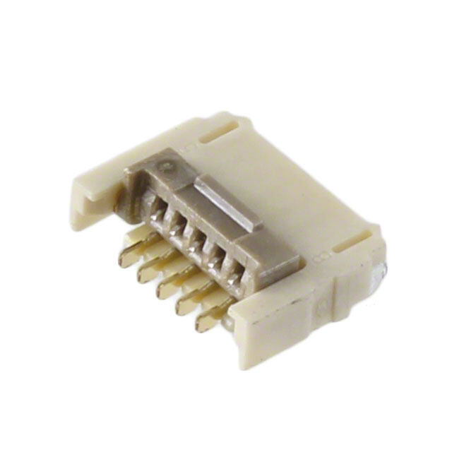
| 产品图片 |
|
| 产品型号 | FGLD12SR6040NA |
| rohs | 无铅 / 符合限制有害物质指令(RoHS)规范要求 |
| 产品系列 | Tomodachi |
| 其它名称 | SY-617CT |
| 功率(W)-制造系列 | 80W |
| 功率(W)-最大值 | 80W |
| 包装 | 剪切带 (CT) |
| 大小/尺寸 | 1.30" 长 x 0.53" 宽 x 0.43" 高(33.0mm x 13.5mm x 10.9mm) |
| 安装类型 | 表面贴装 |
| 封装/外壳 | 模块 |
| 工作温度 | -40°C ~ 85°C |
| 效率 | 91.5% |
| 标准包装 | 1 |
| 特性 | 远程开/关,OCP,OTP,UVLO |
| 特色产品 | http://www.digikey.cn/product-highlights/zh/nonisolated-dcdc-converters/50503 |
| 电压-输入(最大值) | 14.4V |
| 电压-输入(最小值) | 4.5V |
| 电压-输出1 | 0.6 ~ 2 V |
| 电压-输出2 | - |
| 电压-输出3 | - |
| 电压-隔离 | - |
| 电流-输出(最大值) | 40A |
| 类型 | 非隔离 PoL 模块,数字 |
| 输出数 | 1 |


- 商务部:美国ITC正式对集成电路等产品启动337调查
- 曝三星4nm工艺存在良率问题 高通将骁龙8 Gen1或转产台积电
- 太阳诱电将投资9.5亿元在常州建新厂生产MLCC 预计2023年完工
- 英特尔发布欧洲新工厂建设计划 深化IDM 2.0 战略
- 台积电先进制程称霸业界 有大客户加持明年业绩稳了
- 达到5530亿美元!SIA预计今年全球半导体销售额将创下新高
- 英特尔拟将自动驾驶子公司Mobileye上市 估值或超500亿美元
- 三星加码芯片和SET,合并消费电子和移动部门,撤换高东真等 CEO
- 三星电子宣布重大人事变动 还合并消费电子和移动部门
- 海关总署:前11个月进口集成电路产品价值2.52万亿元 增长14.8%


PDF Datasheet 数据手册内容提取
Delivering Next Generation Technology Series FGLD12SR6040*A Data Sh eet 4.5-14.4Vdc Input, 40A, 0.45-2.0Vdc Output The Digital Tomodachi Series of non-isolated dc-dc converters deliver exceptional electrical and thermal performance in DOSA based footprints for Point-of-Load converters. Operating from a 4.5Vdc-14.4Vdc input, these are the converters of choice for Intermediate Bus Architecture (IBA) and Distributed Power Architecture applications that require high efficiency, tight regulation, and high reliability in elevated temperature environments with low airflow. The PMBus interface supports a range of commands to both control and monitor the module. The module also includes the Tunable Loop™ feature that allows the user to optimize the dynamic response of the converter to match the load with reduced amount of output capacitance leading to savings on cost and PWB area. The FGLD12SR6040*A converter of the Tomodachi Features Series delivers 40A of output current at a tightly regulated programmable and PMBus control output voltage of 0.45Vdc to 2.0Vdc. The thermal Compliant to RoHS EU “Directive 2011/65/EU performance of the FGLD12SR6040*A is Delivers up to 40A (80W) best-in-class: Little derating is needed up to 85℃, High efficiency, no heatsink required under natural convection. Negative and Positive ON/OFF logic DOSA based Small size: 33.02 x 13.46 x 10.9mm (1.3 in x 0.53 in x 0.429 in) Applications Tape & reel packaging Programmable output voltage from 0.6V to 2.0V Intermediate Bus Architecture via external resistor. Digitally adjustable down to Telecommunications 0.45Vdc Data/Voice processing Digital interface through the PMBus™ # protocol Distributed Power Architecture Tunable Loop™ to optimize dynamic output Computing (Servers, Workstations) voltage response Test Equipments Flexible output voltage sequencing EZ-SEQUENCE Power Good signal Fixed switching frequency with capability of external synchronization Auto-reset output over-current protection Remote ON/OFF Ability to sink and source current No minimum load required Start up into pre-biased output UL* 60950-1 2nd Ed. Recognized, CSA† C22.2 No. 60950-1-07 Certified, and VDE‡ (EN60950-1 2nd Ed.) (Pending) ISO** 9001 and ISO 14001 certified manufacturing facilities * UL is a registered trademark of Underwriters Laboratories, Inc. † CSA is a registered trademark of Canadian Standards Association. ‡ VDE is a trademark of Verband Deutscher Elektrotechniker e.V. ** ISO is a registered trademark of the International Organization of Standards # The PMBus name and logo are registered trademarks of the System Management Interface Forum (SMIF) Page 1 of 38 Http://www.fdk.com Ver 2.1 Mar. 29, 2016
Delivering Next Generation Technology Series FGLD12SR6040*A Data Sh eet 4.5-14.4Vdc Input, 40A, 0.45-2.0Vdc Output Absolute Maximum Ratings Stresses in excess of the absolute maximum ratings may lead to degradation in performance and reliability of the converter and may result in permanent damage. PARAMETER NOTES MIN TYP MAX UNITS ABSOLUTE MAXIMUM RATINGS1 Input Voltage Continuous -0.3 15 Vdc SEQ, SYNC, Vs+ 7 Vdc CLK, DATA, SMBALERT 3.6 Vdc Operating Temperature Ambient temperature -40 85 °C Storage Temperature -55 125 °C Output Voltage 0.45 2.0 Vdc Electrical Specifications All specifications apply over specified input voltage, output load, and temperature range, unless otherwise noted. PARAMETER NOTES MIN TYP MAX UNITS INPUT CHARACTERISTICS Operating Input Voltage Range 4.5 14.4 Vdc Maximum Input Current Vin=4.5V to 14V, Io-max 24 Adc Input No Load Current Vout=2.0V 104 mA Vout=0.6V 54.7 mA Input Stand-by Current Vin=12V, module disabled 16.4 mA Inrush Transient, I2t 1 A2s Peak-to-peak (5Hz to 20MHz, 1uH source Input Reflected-Ripple Current 90 mAp-p impedance; Vin=0 to 14V, Io-max Input Ripple Rejection (120Hz) -60 dB Input Under Voltage Lockout Turn-on Threshold 3.25 Vdc Turn-off Threshold 2.6 Vdc Hysteresis 0.25 Vdc PMBus Adjustable Input Under Voltage 2.5 14 Vdc Lockout Thresholds Resolution of Adjustable Input Under 500 mV Voltage Threshold Page 2 of 38 Http://www.fdk.com Ver 2.1 Mar. 29, 2016
Delivering Next Generation Technology Series FGLD12SR6040*A Data Sh eet 4.5-14.4Vdc Input, 40A, 0.45-2.0Vdc Output Electrical Specifications (Continued) PARAMETER NOTES MIN TYP MAX UNITS OUTPUT CHARACTERISTICS With 0.1% tolerance for external resistor Output Voltage Set Point -1.0 +1.0 %Vout used to set output voltage (Over all operating input voltage, Output Voltage Range resistive load and temperature -3.0 +3.0 %Vout conditions until end of life) Some output voltages may not be Adjustment Range possible depending on the input voltage 0.6 2.0 Vdc (selected by an external resistor) – see feature description section PMBus Adjustable Output Voltage Range -25 +25 %Vout PMBus Output Voltage Adjustment Step Size 0.4 %Vout Remote Sense Range 0.5 Vdc Output Regulation Line (Vin = min to max) 6 mV Load (Io = min to max) 10 mV Temperature (Tref=min to max) 0.4 %Vout Vin=12V, Io= min to max, Co = Output Ripple and Noise 0.1uF+22uF ceramic capacitors Peak to Peak 5MHz to 20MHz bandwidth 50 100 mVp-p RMS 5MHz to 20MHz bandwidth 20 38 mVrms External Load Capacitance 1 Plus full load (resistive) % Without the Tunable Loop ESR ≥ 1mΩ 6x47 6x47 uF With the Tunable Loop ESR ≥ 0.15mΩ 6x47 7,000 uF ESR ≥ 10mΩ 6x47 8,500 uF Output Current Range (in either sink or source mode) 0 40 Adc Current limit does not operate in sink Output Current Limit Inception (Hiccup mode) 150 % Io-max mode Output Short-Circuit Current Vo ≤ 250mV, Hiccup mode 2..1 Arms Efficiency Vin = 12Vdc, Ta = 25°C, Io = max Vout=1.8Vdc 91.5 % Vout=1.2Vdc 88.5 % Vout=0.6Vdc 81.3 % 1 External capacitors may require using the new Tunable LoopTM feature to ensure that the module is stable as well as getting the best transient response. See the Tunable LoopTM section for details. Page 3 of 38 Http://www.fdk.com Ver 2.1 Mar. 29, 2016
Delivering Next Generation Technology Series FGLD12SR6040*A Data Sh eet 4.5-14.4Vdc Input, 40A, 0.45-2.0Vdc Output Electrical Specifications (Continued) PARAMETER NOTES MIN TYP MAX UNITS Switching Frequency 400 kHz Frequency Synchronization Synchronization Frequency Range 350 480 kHz High Level Input Voltage 2.0 V Low Level Input Voltage 0.4 V Input Current, SYNC 100 nA Minimum Pulse Width, SYNC 100 nS Maximum SYNC rise time 100 nS General Specifications PARAMETER NOTES MIN TYP MAX UNITS Io = 0.8 * Io-max, Ta = 40°C Calculated MTBF 6,498,438 Hours Telecordia Issue 2 Method 1 Case 3 Weight 11.7(0.41) g (oz.) Feature Specifications PARAMETER NOTES MIN TYP MAX UNITS Vin = min to max, open collector or ON/OFF Signal Interface equivalent, Signal reference to GND Positive Logic Logic High (Module ON) Input High Current 10 uA Input High Voltage 3.5 Vin-max V Logic Low (Module OFF) Input Low Current 1 mA Input Low Voltage -0.3 0.4 V On/Off pin is open collector/drain logic input Negative Logic with external pull-up resistor; signal reference to GND Logic High (Module OFF) Input High Current 1 mA Input High Voltage 2 Vin-max V Logic Low (Module ON) Input Low Current 10 uA Input Low Voltage -0.2 0.4 V Page 4 of 38 Http://www.fdk.com Ver 2.1 Mar. 29, 2016
Delivering Next Generation Technology Series FGLD12SR6040*A Data Sh eet 4.5-14.4Vdc Input, 40A, 0.45-2.0Vdc Output Feature Specifications PARAMETER NOTES MIN TYP MAX UNITS Turn-On Delay and Rise Time Vin = Vin-nom, Io = Io-max , Vo to within ±1% of steady state Case 1: On/Off input is enabled and delay from instant at which Vin = Vin-min 1.1 ms then input power is applied until Vo = 10% of Vo-set) Case 2: Input power is applied for at least delay from instant at which Von/Off is one second and then the On/Off input 700 us enabled until Vo = 10% of Vo-set is enabled time for Vo to rise from 10% of Vo-set to Output voltage Rise time 1.5 ms 90% of Vo-set Output voltage overshoot with or without Ta = 25oC, Vin = Vin-min to Vin-max, 3.0 %Vout maximum external capacitance Io = Io-min to Io-max Over Temperature Protection (See Thermal Considerations section) 145 °C PMBus Over Temperature Warning Threshold * 130 °C Vin-min to Vom-max, Io-min to Io-max, Tracking Accuracy VSEQ < Vo Power-Up: 0.5V/ms 100 mV Power-Down: 0.5V/ms 100 mV Input Under Voltage Lockout Turn-on Threshold 4.25 Vdc Turn-off Threshold 3.96 Vdc Hysteresis 0.25 Vdc PMBus Adjustable Input Under Voltage 2.5 14 Vdc Lockout Thresholds Resolution of Adjustable Input Under 500 mV Voltage Threshold PGOOD (Power Good) Signal Interface Open Drain, Vsupply 5VDC Overvoltage threshold for PGOOD ON 108 %Vout Overvoltage threshold for PGOOD OFF 110 %Vout Undervoltage threshold for PGOOD ON 92 %Vout Undervoltage threshold for PGOOD OFF 90 %Vout Pulldown resistance of PGOOD pin 50 Sink current capability into PGOOD pin 5 mA * Over temperature Warning – Warning may not activate before alarm and unit may shutdown before warning. Page 5 of 38 Http://www.fdk.com Ver 2.1 Mar. 29, 2016
Delivering Next Generation Technology Series FGLD12SR6040*A Data Sh eet 4.5-14.4Vdc Input, 40A, 0.45-2.0Vdc Output Digital Interface Specifications PARAMETER NOTES MIN TYP MAX UNITS PMBus Signal Interface Characteristics Input High Voltage (CLK, DATA) 2.1 3.6 V Input Low Voltage (CLK, DATA) 0.8 V Input high level current (CLK, DATA) -10 10 uA Input low level current (CLK, DATA) -10 10 uA Output Low Voltage (CLK, DATA, SMBALERT#) IOUT=2mA 0.4 V Output high level open drain leakage current (DATA, SMBALERT#) VOUT=3.6V 0 10 uA Pin capacitance 0.7 pF PMBus Operating frequency range Slave Mode 10 400 kHz Data hold time Receive Mode 0 nS Transmit Mode 300 nS Data setup time 250 nS Measurement System Characteristics Read delay time 153 192 231 us Output current measurement range 0 40 A Output current measurement resolution 62.5 mA Output current measurement gain accuracy (at 25°C) ±5 % Output current measurement offset 0.1 A Vout measurement range 0 2.0 V Vout measurement resolution 16.25 mV Vout measurement gain accuracy -2 2 LSB Vout measurement offset -3 3 LSB Vout measurement accuracy 70 mV Vin measurement range 0 14.4 V Vin measurement resolution 32.5 mV Vin measurement gain accuracy -2 2 LSB Vin measurement offset -5.5 1.4 LSB Vin measurement accuracy ±3 % Page 6 of 38 Http://www.fdk.com Ver 2.1 Mar. 29, 2016
Delivering Next Generation Technology Series FGLD12SR6040*A Data Sh eet 4.5-14.4Vdc Input, 40A, 0.45-2.0Vdc Output Design Considerations external capacitance values at various Vo and a full load current of 40A. For stable operation of the module, limit the capacitance to less than the Input Filtering maximum output capacitance as specified in the electrical specification table. Optimal performance of The FGLD12SR6040*A converter should be the module can be achieved by using the Tunable connected to a low ac-impedance source. A highly Loop™ feature described later in this data sheet. inductive source can affect the stability of the module. An input capacitance must be placed directly adjacent 40 6x47uF Ext Cap to the input pin of the module, to minimize input ripple voltage and ensure module stability. 8x47uF Ext Cap p) 30 10x47uF Ext Cap To minimize input voltage ripple, ceramic capacitors p- V are recommended at the input of the module. Fig-1 m shows the input ripple voltage for various output e ( 20 voltages at 40A of load current with 4x47uF, 6x47uF ppl or 8x47uF ceramic capacitors and an input of 12V. Ri 10 400 4x22uF Ext Cap k)350 6x22uF Ext Cap 0 p pk-300 8x22uF Ext Cap 0.6 0.8 1 1.2 1.4 1.6 1.8 2 V m e (250 Output Voltage(Volts) g olta200 Fig-2: Output ripple voltage for various output V Ripple 110500 v1loo0alxtda4)g7. euIsFn p cuwet ritavhmo lticea xgcteea rpnisaa cl1i to26Vrsx. 4 a7Stu ctFoh,pe e o 8uBxt4ap7nuudt Fw( 4id0otAhr 50 limited to 20MHz. 0.6 0.8 1 1.2 1.4 1.6 1.8 2 Output Voltage (Volts) Safety Consideration Fig-1: Input ripple voltage for various output voltages with various external ceramic For safety agency approval the power module must capacitors at the input (40A load). Input voltage be installed in compliance with the spacing and is 12V. Scope Bandwidth limited to 20MHz. separation requirements of the end-use safety agency standards, i.e., UL 60950-1 2nd, CSA C22.2 No. 60950-1-07, DIN EN 60950-1:2006 + A11 (VDE0805 Output Filtering Teil 1 + A11):2009-11; EN 60950-1:2006 + A11:2009-03. (Pending) The FGLD12SR6040*A is designed for low output For the converter output to be considered meeting the ripple voltage and will meet the maximum output requirements of safety extra-low voltage (SELV), the ripple specification with 0.1uF ceramic and 47uF input must meet SELV requirements. The power ceramic capacitors at the output of the module. module has extra-low voltage (ELV) outputs when all However, additional output filtering may be required inputs are ELV. by the system designer for a number of reasons. First, there may be a need to further reduce the output The input to these units is to be provided with a fast ripple and noise of the module. Second, the dynamic acting fuse with a maximum rating of 30A, 100V (for response characteristics may need to be customized example, Littlefuse 456 series) in the positive input to a particular load step change. lead. . To reduce the output ripple and improve the dynamic response to a step load change, additional capacitance at the output can be used. Low ESR polymer and ceramic capacitors are recommended to improve the dynamic response of the module. Fig-2 provides output ripple information for different Page 7 of 38 Http://www.fdk.com Ver 2.1 Mar. 29, 2016
Delivering Next Generation Technology Series FGLD12SR6040*A Data Sh eet 4.5-14.4Vdc Input, 40A, 0.45-2.0Vdc Output Analog Feature Descriptions MODULE Remote On/Off VIN+ PWM Enable The module can be turned ON and OFF either by Rpullup using the ON/OFF pin (Analog interface) or through the PMBus interface (Digital). The module can be configured in a number of ways through the PMBus ION/OFF CR1 IPnutlelurnpal interface to react to the two ON/OFF inputs: Module ON/OFF can be controlled only through V + 470 10K ON/OFF the analog interface (digital interface ON/OFF ON/OFF Q1 10K commands are ignored) GND _ Module ON/OFF can be controlled only through the PMBus interface (analog interface is ignored) Fig-3: Circuit configuration for using positive Module ON/OFF can be controlled by either the On/Off logic. analog or digital interface The default state of the module (as shipped from the factory) is to be controlled by the analog interface only. If the digital interface is to be enabled, or the module is to be controlled only through the digital MODULE interface, this change must be made through the PMBus. These changes can be made and written to PWM Enable non-volatile memory on the module so that it is VIN+ remembered for subsequent use. Rpullup Analog ON/OFF Internal Pullup I The FGLD12SR6040*A power modules feature an ON/OFF 470 10K On/Off pin for remote On/Off operation. Two On/Off ON/OFF + Q3 22K V logic options are available. In the Positive Logic ON/OFF Q1 22K On/Off option, (device code suffix “P” - see Ordering 10K Information), the module turns ON during a logic High GND _ on the On/Off pin and turns OFF during a logic Low. With the Negative Logic On/Off option, (device code suffix “N” - see Ordering Information), the module Fig-4: Circuit configuration for using negative turns OFF during logic High and ON during logic Low. On/Off logic. The On/Off signal should be always referenced to ground. For either On/Off logic option, leaving the On/Off pin disconnected will turn the module ON Digital ON/OFF when input voltage is present. Please see the Digital Feature Descriptions section. For positive logic modules, the circuit configuration for using the On/Off pin is shown in Fig-3. Monotonic Start-up and Shut-down For negative logic On/Off modules, the circuit configuration is shown in Fig-4. The module has monotonic start-up and shutdown behavior for any combination of rated input voltage, output current and operating temperature range. Startup into Pre-biased Output The module can start into a prebiased output as long as the prebias voltage is 0.5V less than the set output voltage. Page 8 of 38 Http://www.fdk.com Ver 2.1 Mar. 29, 2016
Delivering Next Generation Technology Series FGLD12SR6040*A Data Sh eet 4.5-14.4Vdc Input, 40A, 0.45-2.0Vdc Output Analog Output Voltage Programming R 12 [kΩ] The output voltage of the module is programmable to TRIM (V -0.6) O-REQ any voltage from 0.6dc to 2.0Vdc by connecting a resistor between the Trim and SIG_GND pins of the Rtrim is the external resistor in kohm module. Certain restrictions apply on the output Vo-req is the desired output voltage voltage set point depending on the input voltage. These are shown in the Output Voltage vs. Input Note that the tolerance of a trim resistor will affect the Voltage Set Point Area plot in Fig-5. The Upper Limit tolerance of the output voltage. Standard 1% or 0.5% curve shows that for output voltages lower than 1V, resistors may suffice for most applications; however, the input voltage must be lower than the maximum of a tighter tolerance can be obtained by using two 14.4V. The Lower Limit curve shows that for output resistors in series instead of one standard value voltages higher than 0.6V, the input voltage needs to resistor. be larger than the minimum of 4.5V. Table 1 provide Rtrim values required for some common output voltages. Table 1: Trim Resistor Value VO-REG [V] RTRIM [kΩ] 0.6 Open 0.9 40 1.0 30 1.2 20 1.5 13.33 1.8 10 Fig-5: Output Voltage vs. Input Voltage Set Point Digital Output Voltage Adjustment Area plot showing limits where the output voltage can be set for different input voltages. Please see the Digital Feature Descriptions section. Remote Sense The power module has a Remote Sense feature to minimize the effects of distribution losses by regulating the voltage between the sense pins (VS+ and VS-). The voltage drop between the sense pins and the Vout and GND pins of the module should not exceed 0.5V. Analog Voltage Margining Output voltage margining can be implemented in the Caution – Do not connect SIG_GND to module by connecting a resistor, Rmargin-up, from GND elsewhere in the layout. the Trim pin to the ground pin for margining-up the output voltage and by connecting a resistor, Fig-6: Circuit configuration for programming Rmargin-down, from the Trim pin to output pin for output voltage using an external resistor. margining-down. Fig-7 shows the circuit configuration for output voltage margining. The POL Programming Tool, available at www.fdk.com under the Downloads section, also calculates the values of Rmargin-up and Without an external resistor between Trim and Rmargin-down for a specific output voltage and % SIG_GND pins, the output of the module will be margin. Please consult your local FDK FAE for 0.6Vdc. To calculate the value of the trim resistor, additional details. Rtrim for a desired output voltage, should be as per the following equation: Page 9 of 38 Http://www.fdk.com Ver 2.1 Mar. 29, 2016
Delivering Next Generation Technology Series FGLD12SR6040*A Data Sh eet 4.5-14.4Vdc Input, 40A, 0.45-2.0Vdc Output Fig-8: Circuit showing connection of the sequencing signal to the SEQ pin. Fig-7: Circuit Configuration for margining Output Voltage. When the scaled down sequencing voltage is applied to the SEQ pin, the output voltage tracks this voltage until the output reaches the set-point voltage. The Digital Output Voltage Margining final value of the sequencing voltage must be set higher than the set-point voltage of the module. The Please see the Digital Feature Descriptions section. output voltage follows the sequencing voltage on a one-to-one basis. By connecting multiple modules Output Voltage Sequencing together, multiple modules can track their output voltages to the voltage applied on the SEQ pin. The power module includes a sequencing feature, The module’s output can track the SEQ pin signal EZSEQUENCE that enables users to implement with slopes of up to 0.5V/msec during power-up or various types of output voltage sequencing in their power-down. applications. This is accomplished via an additional sequencing pin. When not using the sequencing To initiate simultaneous shutdown of the modules, the feature, leave it unconnected. SEQ pin voltage is lowered in a controlled manner. The output voltage of the modules tracks the voltages The voltage applied to the SEQ pin should be scaled below their set-point voltages on a one-to-one basis. down by the same ratio as used to scale the output A valid input voltage must be maintained until the voltage down to the reference voltage of the module. tracking and output voltages reach ground potential. This is accomplished by an external resistive divider connected across the sequencing voltage before it is Note that in all digital Tomodachi series of modules, fed to the SEQ pin as shown in Fig-8. In addition, a the PMBus Output Undervoltage Fault will be tripped small capacitor (suggested value 100pF) should be when sequencing is employed. This will be detected connected across the lower resistor R1. using the STATUS_WORD and STATUS_VOUT PMBus commands. In addition, the SMBALERT# For all Tomodachi modules, the minimum signal will be asserted low as occurs for all faults and recommended delay between the ON/OFF signal and warnings. To avoid the module shutting down due to the sequencing signal is 10ms to ensure that the the Output Undervoltage Fault, the module must be module output is ramped up according to the set to continue operation without interruption as the sequencing signal. This ensures that the module response to this fault (see the description of the soft-start routine is completed before the sequencing PMBus command VOUT_UV_FAULT_RESPONSE signal is allowed to ramp up. for additional information). Page 10 of 38 Http://www.fdk.com Ver 2.1 Mar. 29, 2016
Delivering Next Generation Technology Series FGLD12SR6040*A Data Sh eet 4.5-14.4Vdc Input, 40A, 0.45-2.0Vdc Output Over-Current Protection using the external signal applied to the SYNC pin of the module as shown in Fig-9, with the converter To provide protection in a fault (output overload) being synchronized by the rising edge of the external condition, the unit is equipped with internal signal. The Electrical Specifications table specifies current-limiting circuitry and can endure current the requirements of the external SYNC signal. If the limiting continuously. At the point of current-limit SYNC pin is not used, the module should free run at inception, the unit enters hiccup mode. The unit the default switching frequency. If synchronization operates normally once the output current is brought is not being used, connect the SYNC pin to GND. back into its specified range. Digital Adjustable Overcurrent Warning Please see the Digital Feature Descriptions section. Over-Temperature Protection To provide protection in a fault condition, the unit is equipped with a thermal shutdown circuit. The unit will shut down if the over-temperature threshold of 145ºC (typ) is exceeded at the thermal reference point Tref. Fig-9: External source connections to Once the unit goes into thermal shutdown it will then synchronize switching frequency of the module. wait to cool before attempting to restart. Paralleling with Active Load Sharing (-P Digital Temperature Status via PMBus Option) Please see the Digital Feature Descriptions section. For additional power requirements, the FGLD12SR6040*A power module is also equipped Digitally Adjustable Output Over and Under with paralleling capability. Up to five modules can be Voltage Protection configured in parallel, with active load sharing. To implement paralleling, the following conditions Please see the Digital Feature Descriptions section. must be satisfied. All modules connected in parallel must be Input Under-Voltage Lockout (UVLO) frequency synchronized where they are switching at the same frequency. This is done by using the SYNC function of the module and connecting to At input voltages below the input under-voltage an external frequency source. Modules can be lockout limit, the module operation is disabled. The interleaved to reduce input ripple/filtering module will begin to operate at an input voltage above requirements. the under-voltage lockout turn-on threshold. The share pins of all units in parallel must be connected together. The path of these Digitally Adjustable Input Undervoltage connections should be as direct as possible. Lockout The remote sense connections to all modules should be made that to the same points for the Please see the Digital Feature Descriptions section. output, i.e. all VS+ and VS- terminals for all modules are connected to the power bus at the same points. Digitally Adjustable Power Good Thresholds Some special considerations apply for design of Please see the Digital Feature Descriptions section. converters in parallel operation: When sizing the number of modules required for Synchronization parallel operation, take note of the fact that current sharing has some tolerance. In addition, under transient conditions such as a dynamic The module switching frequency can be synchronized load change and during startup, all converter to a signal with an external frequency within a output currents will not be equal. To allow for specified range. Synchronization can be done by Page 11 of 38 Http://www.fdk.com Ver 2.1 Mar. 29, 2016
Delivering Next Generation Technology Series FGLD12SR6040*A Data Sh eet 4.5-14.4Vdc Input, 40A, 0.45-2.0Vdc Output such variation and avoid the likelihood of a Measuring Output Current, Output Voltage converter shutting off due to a current overload, and Input Voltage the total capacity of the paralleled system should be no more than 90% of the sum of the individual Please see the Digital Feature Descriptions section. converters. As an example, for a system of four FGLS converters in parallel, the total current drawn should be less that 90% of (3 x 40A), i.e. Dual Layout less than 108 A. Similarly, four units can support a load less than 144A. Identical dimensions and pin layout of Analog and All modules should be turned ON and OFF Digital Tomodachi modules permit migration from together. This is so that all modules come up at one to the other without needing to change the layout. the same time avoiding the problem of one In both cases the trim resistor is connected between converter sourcing current into the other leading trim and signal ground. to an overcurrent trip condition. To ensure that all modules come up simultaneously, the on/off pins Power Good of all paralleled converters should be tied together The module provides a Power Good (PGOOD) signal and the converters enabled and disabled using that is implemented with an open-drain output to the on/off pin. Note that this means that indicate that the output voltage is within the regulation converters in parallel cannot be digitally turned limits of the power module. The PGOOD signal will be ON as that does not ensure that all modules de-asserted to a low state if any condition such as being paralleled turn on at the same time. overtemperature, overcurrent or loss of regulation If digital trimming is used to adjust the overall occurs that would result in the output voltage going output voltage, the adjustments need to be made ±10% outside the setpoint value. The PGOOD in a series of small steps to avoid shutting down terminal can be connected through a pullup resistor the output. Each step should be no more than (suggested value 100K) to a source of 5VDC or 20mV for each module. For example, to adjust lower. the overall output voltage in a setup with two modules (A and B) in parallel from 1V to 1.1V, module A would be adjusted from 1.0 to 1.02V Tunable Loop™ followed by module B from 1.0 to 1.02V, then each module in sequence from 1.02 to 1.04V and The module has a feature that optimizes transient so on until the final output voltage of 1.1V is response of the module called Tunable Loop™ reached. If the Sequencing function is being used to External capacitors are usually added to the output of start-up and shut down modules and the module the module for two reasons: to reduce output ripple is being held to 0V by the tracking signal then and noise (see Fig-2) and to reduce output voltage there may be small deviations on the module deviations from the steady-state value in the output. This is due to controller duty cycle presence of dynamic load current changes. Adding limitations encountered in trying to hold the external capacitance however affects the voltage voltage down near 0V. control loop of the module, typically causing the loop The share bus is not designed for redundant to slow down with sluggish response. Larger values of operation and the system will be non-functional external capacitance could also cause the module to upon failure of one of the units when multiple become unstable. units are in parallel. In particular, if one of the converters shuts down during operation, the other The Tunable Loop™ allows the user to externally converters may also shut down due to their adjust the voltage control loop to match the filter outputs hitting current limit. In such a situation, network connected to the output of the module. The unless a coordinated restart is ensured, the Tunable Loop™ is implemented by connecting a system may never properly restart since different series R-C between the SENSE and TRIM pins of the converters will try to restart at different times module, as shown in Fig-10. This R-C allows the user causing an overload condition and subsequent to externally adjust the voltage loop feedback shutdown. This situation can be avoided by compensation of the module. having an external output voltage monitor circuit that detects a shutdown condition and forces all converters to shut down and restart together. When not using the active load share feature, share pins should be left unconnected. Page 12 of 38 Http://www.fdk.com Ver 2.1 Mar. 29, 2016
Delivering Next Generation Technology Series FGLD12SR6040*A Data Sh eet 4.5-14.4Vdc Input, 40A, 0.45-2.0Vdc Output Table 3: Recommended values of R TUNE and CTUNE to obtain transient deviation of 2% of Vout for a 20A step load with Vin=12V. Vo 1.8V 1.2V 0.6V 4x47uF+ 4x47uF+ 4x47uF+ Co 6x330uF 11x330uF 12x680uF Polymer Polymer Polymer R 220Ω 200 Ω 180 Ω TUNE C 5600pF 12nF 47nF TUNE △V 34mV 22mV 12mV Note: The capacitors used in the Tunable Loop Fig-10: Circuit diagram showing connection of tables are 47 uF/3 mΩ ESR ceramic, 330 uF/12 mΩ R and C to tune the control loop of the TUNE TUNE ESR polymer capacitor and 680uF/12 mΩ polymer module. capacitor. Recommended values of R and C for different TUNE TUNE output capacitor combinations are given in Table 2. Table 2 shows the recommended values of R and TUNE C for different values of ceramic output capacitors TUNE up to 1,000uF that might be needed for an application to meet output ripple and noise requirements. Selecting R and C according to Table 2 will TUNE TUNE ensure stable operation of the module. In applications with tight output voltage limits in the presence of dynamic current loading, additional output capacitance will be required. Table 3 lists recommended values of R and C in order to TUNE TUNE meet 2% output voltage deviation limits for some common output voltages in the presence of a 10A to 40A step change (50% of full load), with an input voltage of 12V. Please contact your FDK technical representative to obtain more details of this feature as well as for guidelines on how to select the right value of external R-C to tune the module for best transient performance and stable operation for other output capacitance values. Table 2: General recommended value of R TUNE and C for Vin=12V and various external TUNE ceramic capacitor combinations. Co 6x47uF 8x47uF 10x47uF 12x47uF 20x47uF R 330Ω 330Ω 330Ω 330Ω 200Ω TUNE C 330pF 820pF 1200pF 1500pF 3300pF TUNE Page 13 of 38 Http://www.fdk.com Ver 2.1 Mar. 29, 2016
Delivering Next Generation Technology Series FGLD12SR6040*A Data Sh eet 4.5-14.4Vdc Input, 40A, 0.45-2.0Vdc Output Digital Feature Description set using resistors connected from the ADDR0 and ADDR1 pins to SIG_GND. Note that some of these addresses (0, 1, 2, 3, 4, 5, 6, 7, 8, 9, 10, 11 12, 40, 44, PMBus Interface Capability 45, 55 in decimal) are reserved according to the SMBus specifications and may not be useable. The The 40A Digital Tomodachi power modules have a address is set in the form of two octal (0 to 7) digits, PMBus interface that supports both communication with each pin setting one digit. The ADDR1 pin sets and control. The PMBus Power Management Protocol the high order digit and ADDR0 sets the low order Specification can be obtained from www.pmbus.org. digit. The resistor values suggested for each digit are The modules support a subset of version 1.1 of the shown in Table 4 (1% tolerance resistors are specification (see Table 6 for a list of the specific recommended). Note that if either address resistor commands supported). Most module parameters can value is outside the range specified in Table 4, the be programmed using PMBus and stored as defaults module will respond to address 127. for later use. Table 4: All communication over the module PMBus interface Digit Resistor Value [kΩ] must support the Packet Error Checking (PEC) scheme. The PMBus master must generate the 0 10 correct PEC byte for all transactions, and check the 1 15.4 PEC byte returned by the module. 2 23.7 The module also supports the SMBALERT# response protocol whereby the module can alert the bus master 3 36.5 if it wants to talk. For more information on the 4 54.9 SMBus alert response protocol, see the System 5 84.5 Management Bus (SMBus) specification. 6 130 The module has non-volatile memory that is used to store configuration settings. Not all settings 7 200 programmed into the device are automatically saved into this non-volatile memory, only those specifically identified as capable of being stored can be saved The user must know which I2C addresses are (see Table 6 for which command parameters can be reserved in a system for special functions and set the saved to non-volatile storage). address of the module to avoid interfering with other system operations. Both 100kHz and 400kHz bus speeds are supported by the module. Connection for PMBus Data Format the PMBus interface should follow the High Power DC specifications given in section 3.1.3 in the SMBus For commands that set thresholds, voltages or report specification V2.0 for the 400kHz bus speed or the such quantities, the module supports the “Linear” data Low Power DC specifications in section 3.1.2. The format among the three data formats supported by complete SMBus specification is available from the PMBus. The Linear Data Format is a two byte value SMBus web site, smbus.org. with an 11-bit, two’s complement mantissa and a 5-bit, two’s complement exponent. The format of the two data bytes is shown below: ADDR1 Data Byte High Data Byte Low ADDR0 7 6 5 4 3 2 1 0 7 6 5 4 3 2 1 0 R R ADDR0 ADDR1 Exponent Mantissa MSB MSB SIG_GND The value is of the number is then given by Fig-11: Circuit showing connection of resistors Value = Mantissa x 2Exponent used to set the PMBus address of the module. PMBus Addressing The power module can be addressed through the PMBus using a device address. The module has 64 possible addresses (0 to 63 in decimal) which can be Page 14 of 38 Http://www.fdk.com Ver 2.1 Mar. 29, 2016
Delivering Next Generation Technology Series FGLD12SR6040*A Data Sh eet 4.5-14.4Vdc Input, 40A, 0.45-2.0Vdc Output PMBus Enabled On/Off PMBus Adjustable Soft Start Rise Time The module can also be turned on and off via the The soft start rise time can be adjusted in the module PMBus interface. The OPERATION command is used via PMBus. When setting this parameter, make sure to actually turn the module on and off via the PMBus, that the charging current for output capacitors can be while the ON_OFF_CONFIG command configures delivered by the module in addition to any load the combination of analog ON/OFF pin input and current to avoid nuisance tripping of the overcurrent PMBus commands needed to turn the module on and protection circuitry during startup. The TON_RISE off. Bit [7] in the OPERATION command data byte command sets the rise time in ms, and allows enables the module, with the following functions: choosing soft start times between 600us and 9ms, with possible values listed in Table 5. Note that the 0 : Output is disabled exponent is fixed at -4 (decimal) and the upper two 1 : Output is enabled bits of the mantissa are also fixed at 0. This module uses the lower five bits of the ON_OFF_CONFIG data byte to set various ON/OFF Table 5 options as follows: Rise Time Exponent Mantissa 600us 11100 00000001010 900us 11100 00000001110 Bit Position 4 3 2 1 0 1.2ms 11100 00000010011 Access r/w r/w r/w r/w r 1.8ms 11100 00000011101 Function PU CMD CPR POL CPA Default Value 1 0 1 1 1 2.7ms 11100 00000101011 4.2ms 11100 00001000011 PU: Sets the default to either operate any time input 6.0ms 11100 00001100000 power is present or for the ON/OFF to be controlled 9.0ms 11100 00010010000 by the analog ON/OFF input and the PMBus OPERATION command. This bit is used together with Output Voltage Adjustment Using the the CP, CMD and ON bits to determine startup. PMBus Bit Value Action Module powers up any time power is The VOUT_SCALE_LOOP parameter is important for 0 present regardless of state of the analog a number of PMBus commands related to output ON/OFF pin voltage trimming, margining, over/under voltage Module does not power up until protection and the PGOOD thresholds. The output commanded by the analog ON/OFF pin 1 and the OPERATION command as voltage of the module is set as the combination of the programmed in bits [2:0] of the voltage divider formed by RTrim and a 20kΩ upper ON_OFF_CONFIG register. divider resistor inside the module, and the internal reference voltage of the module. The reference voltage V is nominally set at 600mV, and the CMD: The CMD bit controls how the device responds REF output regulation voltage is then given by to the OPERATION command. 20000RTrim Bit Value Action V V 0 Module ignores the ON bit in the OUT RTrim REF OPERATION command Module responds to the ON bit in the 1 Hence the module output voltage is dependent on the OPERATION command value of RTrim which is connected external to the module. The information on the output voltage divider CPR: Sets the response of the analog ON/OFF pin. ratio is conveyed to the module through the This bit is used together with the CMD, PU and ON VOUT_SCALE_LOOP parameter which is calculated bits to determine startup. as follows: Bit Value Action RTrim Module ignores the analog ON/OFF pin, VOUT_SCALE_LOOP 20000RTrim 0 i.e. ON/OFF is only controlled through the PMBUS via the OPERATION command Module requires the analog ON/OFF pin The VOUT_SCALE_LOOP parameter is specified 1 to be asserted to start the unit using the “Linear” format and two bytes. The upper five bits [7:3] of the high byte are used to set the exponent which is fixed at –9 (decimal). The remaining three bits of the high byte [2:0] and the Page 15 of 38 Http://www.fdk.com Ver 2.1 Mar. 29, 2016
Delivering Next Generation Technology Series FGLD12SR6040*A Data Sh eet 4.5-14.4Vdc Input, 40A, 0.45-2.0Vdc Output eight bits of the lower byte are used for the mantissa. The default value of the mantissa is 00100000000 Note that the sum of the margin and trim voltages corresponding to 256 (decimal), corresponding to a cannot be outside the ±25% window around the divider ratio of 0.5. The maximum value of the nominal output voltage. The data associated with mantissa is 512 corresponding to a divider ratio of 1. VOUT_MARGIN_HIGH and VOUT_MARGIN_LOW Note that the resolution of the VOUT_SCALE_LOOP can be stored to non-volatile memory using the command is 0.2%. STORE_DEFAULT_ALL command. When PMBus commands are used to trim or margin The module is commanded to go to the margined high the output voltage, the value of V is what is or low voltages using the OPERATION command. REF changed inside the module, which in turn changes the Bits [5:2] are used to enable margining as follows: regulated output voltage of the module. 00XX : Margin Off 0101 : Margin Low (Ignore Fault) The nominal output voltage of the module can be 0110 : Margin Low (Act on Fault) adjusted with a minimum step size of 0.4% over a 1001 : Margin High (Ignore Fault) ±25% range from nominal using the VOUT_TRIM 1010 : Margin High (Act on Fault) command over the PMBus. The VOUT_TRIM command is used to apply a fixed PMBus Adjustable Overcurrent Warning offset voltage to the output voltage command value using the “Linear” mode with the exponent fixed at – The module can provide an overcurrent warning via 10 (decimal). The value of the offset voltage is given the PMBus. The threshold for the overcurrent warning by can be set using the parameter V VOUT_TRIM210 IOUT_OC_WARN_LIMIT. This command uses the OUT(offset) “Linear” data format with a two byte data word where the upper five bits [7:3] of the high byte represent the This offset voltage is added to the voltage set through exponent and the remaining three bits of the high byte the divider ratio and nominal VREF to produce the [2:0] and the eight bits in the low byte represent the trimmed output voltage. The valid range in two’s mantissa. The exponent is fixed at –1 (decimal). The complement for this command is –4000h to 3999h. upper five bits of the mantissa are fixed at 0 while the The high order two bits of the high byte must both be lower six bits are programmable with a default value either 0 or 1. If a value outside of the +/-25% of 55.5A (decimal). The resolution of this warning limit adjustment range is given with this command, the is 500mA. The value of the IOUT_OC_WARN_LIMIT module will set it’s output voltage to the nominal value can be stored to non-volatile memory using the (as if VOUT_TRIM had been set to 0), assert STORE_DEFAULT_ALL command. SMBALRT#, set the CML bit in STATUS_BYTE and the invalid data bit in STATUS_CML. Temperature Status via PMBus Output Voltage Margining Using the PMBus The module can provide information related to temperature of the module through the The module can also have its output voltage STATUS_TEMPERATURE command. The command margined via PMBus commands. The command returns information about whether the pre-set over VOUT_MARGIN_HIGH sets the margin high voltage, temperature fault threshold and/or the warning while the command VOUT_MARGIN_LOW sets the threshold have been exceeded. margin low voltage. Both the VOUT_MARGIN_HIGH and VOUT_MARGIN_LOW commands use the “Linear” mode with the exponent fixed at –10 PMBus Adjustable Output Over and Under (decimal). Two bytes are used for the mantissa with Voltage Protection the upper bit [7] of the high byte fixed at 0. The actual margined output voltage is a combination of the The module has output over and under voltage VOUT_MARGIN_HIGH or VOUT_MARGIN_LOW protection capability. The PMBus command and the VOUT_TRIM values as shown below. VOUT_OV_FAULT_LIMIT is used to set the output V over voltage threshold from four possible values: OUT(MH) 108%, 110%, 112% or 115% of the commanded (VOUT_MARGIN_HIGHVOUT_TRIM)210 output voltage. The command V VOUT_UV_FAULT_LIMIT sets the threshold that OUT(ML) causes an output under voltage fault and can also be (VOUT_MARGIN_LOWVOUT_TRIM)210 selected from four possible values: 92%, 90%, 88% or Page 16 of 38 Http://www.fdk.com Ver 2.1 Mar. 29, 2016
Delivering Next Generation Technology Series FGLD12SR6040*A Data Sh eet 4.5-14.4Vdc Input, 40A, 0.45-2.0Vdc Output 85%. The default values are 112% and 88% of bits represent the exponent (fixed at -2) and the commanded output voltage. Both commands use two remaining 11 bits represent the mantissa. For the data bytes formatted as two’s complement binary mantissa, the four most significant bits are fixed at 0. integers. The “Linear” mode is used with the exponent fixed to –10 (decimal) and the effective over or under Power Good voltage trip points given by: V (VOUT_OV_FAULT_LIMIT)210 The module provides a Power Good (PGOOD) signal OUT(OV_REQ) that is implemented with an open-drain output to V (VOUT_UV_FAULT_LIMIT)210 OUT(UV_REQ) indicate that the output voltage is within the regulation limits of the power module. The PGOOD signal will be Values within the supported range for over and de-asserted to a low state if any condition such as undervoltage detection thresholds will be set to the overtemperature, overcurrent or loss of regulation nearest fixed percentage. Note that the correct value occurs that would result in the output voltage going for VOUT_SCALE_LOOP must be set in the module outside the specified thresholds. The PGOOD for the correct over or under voltage trip points to be thresholds are user selectable via the PMBus (the calculated. default values are as shown in the Feature In addition to adjustable output voltage protection, the Specifications Section). Each threshold is set up 40A Digital Tomodachi module can also be symmetrically above and below the nominal value. programmed for the response to the fault. The The POWER_GOOD_ON command sets the output VOUT_OV_FAULT_RESPONSE and voltage level above which PGOOD is asserted (lower VOUT_UV_FAULT_RESPONSE commands specify threshold). For example, with a 1.2V nominal output the response to the fault. Both these commands use a voltage, the POWER_GOOD_ON threshold can set single data byte with the possible options as shown the lower threshold to 1.14 or 1.1V. Doing this will below. automatically set the upper thresholds to 1.26 or 1.3V. 1. Continue operation without interruption (Bits [7:6] The POWER_GOOD_OFF command sets the level = 00, Bits [5:3] = xxx) below which the PGOOD command is de-asserted. 2. Continue for four switching cycles and then shut This command also sets two thresholds symmetrically down if the fault is still present, followed by no placed around the nominal output voltage. Normally, restart or continuous restart (Bits [7:6] = 01, the POWER_GOOD_ON threshold is set higher than Bits [5:3] = 000 means no restart, Bits [5:3] = 111 the POWER_GOOD_OFF threshold. means continuous restart) 3. Immediate shut down followed by no restart or Both POWER_GOOD_ON and continuous restart (Bits [7:6] = 10, Bits [5:3] = POWER_GOOD_OFF commands use the “Linear” 000 means no restart, Bits [5:3] = 111 means format with the exponent fixed at –10 (decimal). The continuous restart). two thresholds are given by 4. Module output is disabled when the fault is V (POWER_GOOD_ON)210 present and the output is enabled when the fault OUT(PGOOD_ON) no longer exists (Bits [7:6] = 11, Bits [5:3] = xxx). V (POWER_GOOD_OFF)210 Note that separate response choices are possible for OUT(PGOOD_OFF) output over voltage or under voltage faults. Both commands use two data bytes with bit [7] of the high byte fixed at 0, while the remaining bits are r/w and used to set the mantissa using two’s complement PMBus Adjustable Input Undervoltage representation. Both commands also use the Lockout VOUT_SCALE_LOOP parameter so it must be set correctly. The default value of POWER_GOOD_ON is The module allows adjustment of the input under set at 1.1035V and that of the POWER_GOOD_OFF voltage lockout and hysteresis. The command is set at 1.08V. The values associated with these VIN_ON allows setting the input voltage turn on commands can be stored in non-volatile memory threshold, while the VIN_OFF command sets the using the STORE_DEFAULT_ALL command. input voltage turn off threshold. For the VIN_ON The PGOOD terminal can be connected through a command, possible values are 3.5V to 14V in 0.5V pullup resistor (suggested value 100K) to a source steps. For the VIN_OFF command, possible values of 5VDC or lower. are 3V to 14V in 0.5V steps. If other values are entered for either command, they will be mapped to the closest of the allowed values. Both the VIN_ON and VIN_OFF commands use the “Linear” format with two data bytes. The upper five Page 17 of 38 Http://www.fdk.com Ver 2.1 Mar. 29, 2016
Delivering Next Generation Technology Series FGLD12SR6040*A Data Sh eet 4.5-14.4Vdc Input, 40A, 0.45-2.0Vdc Output Measurement of Output Current, Output where IOUT_CORR is the temperature corrected value of Voltage and Input Voltage the current measurement, IREAD_OUT is the module current measurement value, T is the temperature of IND the inductor winding on the module. Since it may be The module is capable of measuring key module difficult to measure T , it may be approximated by parameters such as output current and voltage and IND an estimate of the module temperature. input voltage and providing this information through the PMBus interface. Roughly every 200us, the module makes 16 measurements each of output Measuring Output Voltage Using the PMBus current, voltage and input voltage. Average values of of these 16 measurements are then calculated and The module can provide output voltage information placed in the appropriate registers. The values in the using the READ_VOUT command. The command registers can then be read using the PMBus interface. returns two bytes of data all representing the mantissa while the exponent is fixed at -10 (decimal). Measuring Output Current Using the PMBus During manufacture of the module, offset and gain correction values are written into the non-volatile The module measures current by using the inductor memory of the module. The command winding resistance as a current sense element. The VOUT_CAL_OFFSET can be used to read and/or inductor winding resistance is then the current gain write the offset (two bytes consisting of a 16-bit factor used to scale the measured voltage into a mantissa in two’s complement format) while the current reading. This gain factor is the argument of exponent is always fixed at -10 (decimal). The the IOUT_CAL_GAIN command, and consists of two allowed range for this offset correction is -125 to bytes in the linear data format. The exponent uses the 124mV. The command VOUT_CAL_GAIN can be upper five bits [7:3] of the high data byte in two-s used to read and/or write the gain correction - two complement format and is fixed at –15 (decimal). bytes consisting of a five-bit exponent (fixed at -8) and The remaining 11 bits in two’s complement binary a 11-bit mantissa. The range of this correction factor format represent the mantissa. During manufacture, is -0.125V to +0.121V, with a resolution of 0.004V. each module is calibrated by measuring and storing The corrected output voltage reading is then given by: the current gain factor into non-volatile storage. The current measurement accuracy is also improved VOUT(Final) by each module being calibrated during manufacture [V (Initial)(1VOUT_CAL_GAIN)] OUT with the offset in the current reading. The VOUT_CAL_OFFSET IOUT_CAL_OFFSET command is used to store and read the current offset. The argument for this command consists of two bytes composed of a 5-bit Measuring Input Voltage Using the PMBus exponent (fixed at -4d) and a 11-bit mantissa. This command has a resolution of 62.5mA and a range of The module can provide output voltage information -4000mA to +3937.5mA. using the READ_VIN command. The command returns two bytes of data in the linear format. The The READ_IOUT command provides module upper five bits [7:3] of the high data form the two’s average output current information. This command complement representation of the mantissa which is only supports positive or current sourced from the fixed at –5 (decimal). The remaining 11 bits are used module. If the converter is sinking current a reading of for two’s complement representation of the mantissa, 0 is provided. The READ_IOUT command returns two with the 11th bit fixed at zero since only positive bytes of data in the linear data format. The exponent numbers are valid. uses the upper five bits [7:3] of the high data byte in two-s complement format and is fixed at –4 (decimal). During module manufacture, offset and gain The remaining 11 bits in two’s complement binary correction values are written into the non-volatile format represent the mantissa with the 11th bit fixed at memory of the module. The command 0 since only positive numbers are considered valid. VIN_CAL_OFFSET can be used to read and/or write the offset - two bytes consisting of a five-bit exponent Note that the current reading provided by the module (fixed at -5) and a 11-bit mantissa in two’s is not corrected for temperature. The temperature complement format. The allowed range for this offset corrected current reading for module temperature correction is -2 to 1.968V, and the resolution is 32mV. T can be estimated using the following equation. Module The command VIN_CAL_GAIN can be used to read I and/or write the gain correction - two bytes consisting I READ_OUT OUT,CORR of a five-bit exponent (fixed at -8) and a 11-bit 1[(T 30)0.00393] IND mantissa. The range of this correction factor is Page 18 of 38 Http://www.fdk.com Ver 2.1 Mar. 29, 2016
Delivering Next Generation Technology Series FGLD12SR6040*A Data Sh eet 4.5-14.4Vdc Input, 40A, 0.45-2.0Vdc Output -0.125V to +0.121V, with a resolution of 0.004V. STATUS_VOUT: Returns one byte of information The corrected output voltage reading is then given by: relating to the status of the module’s output voltage related faults. V (Final) IN [V (Initial)(1VIN_CAL_GAIN)] Bit Default IN Flag Position Value VIN_CAL_OFFSET 7 VOUT OV Fault 0 6 X 0 5 X 0 Reading the Status of the Module using the 4 VOUT UV Fault 0 PMBus 3 X 0 2 X 0 The module supports a number of PMBus status 1 X 0 information commands. However, not all features are 0 X 0 supported in these commands. A 1 in the bit position indicates the fault that is flagged. STATUS_IOUT: Returns one byte of information relating to the status of the module’s output voltage STATUS_BYTE: Returns one byte of information with related faults. a summary of the most critical device faults. Bit Default Bit Default Flag Flag Position Value Position Value 7 X 0 7 IOUT OC Fault 0 6 OFF 0 6 X 0 5 VOUT Overvoltage 0 5 IOUT OC Warning 0 4 IOUT Overcurrent 0 4 X 0 3 VIN Undervoltage 0 3 X 0 2 Temperature 0 2 X 0 1 CML (Comm. Memory Fault) 0 1 X 0 0 None of the above 0 0 X 0 STATUS_WORD: Returns two bytes of information STATUS_TEMPERATURE: Returns one byte of with a summary of the module’s fault/warning information relating to the status of the module’s conditions. temperature related faults. Low Byte Bit Default Bit Default Flag Flag Position Value Position Value 7 X 0 7 OT Fault 0 6 OFF 0 6 OT Warning 0 5 VOUT Overvoltage 0 5 X 0 4 IOUT Overcurrent 0 4 X 0 3 VIN Undervoltage 0 3 X 0 2 Temperature 0 2 X 0 1 CML (Comm. Memory Fault) 0 1 X 0 0 None of the above 0 0 X 0 High Byte STATUS_CML: Returns one byte of information Bit Default relating to the status of the module’s communication Flag Position Value related faults. 7 VOUT fault or warning 0 6 IOUT fault or warning 0 Bit Default Flag 5 X 0 Position Value 4 X 0 Invalid/Unsupported 7 0 3 POWER_GOOD# (is negated) 0 Command 2 X 0 Invalid/Unsupported 6 0 1 X 0 Command 0 X 0 5 Packet Error Check Failed 0 4 X 0 Page 19 of 38 Http://www.fdk.com Ver 2.1 Mar. 29, 2016
Delivering Next Generation Technology Series FGLD12SR6040*A Data Sh eet 4.5-14.4Vdc Input, 40A, 0.45-2.0Vdc Output 3 X 0 2 X 0 1 Other Communication Fault 0 0 X 0 MFR_VIN_MIN: Returns minimum input voltage as two data bytes of information in Linear format (upper five bits are exponent – fixed at -2, and lower 11 bits are mantissa in two’s complement format – fixed at 12) MFR_VOUT_MIN: Returns minimum output voltage as two data bytes of information in Linear format (upper five bits are exponent – fixed at -10, and lower 11 bits are mantissa in two’s complement format – fixed at 614) MFR_SPECIFIC_00: Returns information related to the type of module. Bits [7:2] in the Low Byte indicate the module type (000100 corresponds to the FGLD12SR6040 series of module). Bit [1:0] in the High Byte are used to indicate the manufacturer ID, with 01 reserved for FDK. Low Byte Bit Default Flag Position Value 7:2 Module Name 000100 1:0 Reserved 00 High Byte Bit Default Flag Position Value 7:2 Reserved None 1:0 Manufacturer ID 01 Page 20 of 38 Http://www.fdk.com Ver 2.1 Mar. 29, 2016
Delivering Next Generation Technology Series FGLD12SR6040*A Data Sh eet 4.5-14.4Vdc Input, 40A, 0.45-2.0Vdc Output Summary of Supported PMBus Commands Please refer to the PMBus 1.1 specification for more details of these commands. Table 6 Non-Volatile Hex Command Brief Description Memory Code Storage Turn Module on or off. Also used to margin the output voltage Format Unsigned Binary Bit Position 7 6 5 4 3 2 1 0 01 OPERATION Access r/w r r/w r/w r/w r/w r r Function On X Margin X X Default Value 0 0 0 0 0 0 X X Configures the ON/OFF functionality as a combination of analog ON/OFF pin and PMBus commands Format Unsigned Binary 02 ON_OFF_CONFIG Bit Position 7 6 5 4 3 2 1 0 YES Access r r r r/w r/w r/w r/w r Function X X X pu cmd cpr pol cpa Default Value 0 0 0 1 0 1 1 1 Clear any fault bits that may have been set, also releases the SMBALERT# 03 CLEAR_FAULTS signal if the device has been asserting it. Used to control writing to the module via PMBus. Copies the current register setting in the module whose command code matches the value in the data byte into non-volatile memory (EEPROM) on the module Format Unsigned Binary Bit Position 7 6 5 4 3 2 1 0 Access r/w r/w r/w x x x x x Function bit7 bit6 bit5 X X X X X Default Value 0 0 0 X X X X X 10 WRITE_PROTECT Bit5: 0 – Enables all writes as permitted in bit6 or bit7 YES 1 – Disables all writes except the WRITE_PROTECT, OPERATION and ON_OFF_CONFIG (bit 6 and bit7 must be 0) Bit 6: 0 – Enables all writes as permitted in bit5 or bit7 1 – Disables all writes except for the WRITE_PROTECT and OPERATION commands (bit5 and bit7 must be 0) Bit7: 0 – Enables all writes as permitted in bit5 or bit6 1 – Disables all writes except for the WRITE_PROTECT command (bit5 and bit6 must be 0) Copies all current register settings in the module into non-volatile memory 11 STORE_DEFAULT_ALL (EEPROM) on the module. Takes about 50ms for the command to execute. Restores all current register settings in the module from values in the module 12 RESTORE_DEFAULT_ALL non-volatile memory (EEPROM) Copies the current register setting in the module whose command code matches the value in the data byte into non-volatile memory (EEPROM) on the module 13 STORE_DEFAULT_CODE Bit Position 7 6 5 4 3 2 1 0 Access w w w w w w w w Function Command code Restores the current register setting in the module whose command code matches the value in the data byte from the value in the module non-volatile memory (EEPROM) 14 RESTORE_DEFAULT_CODE Bit Position 7 6 5 4 3 2 1 0 Access w w w w w w w w Function Command code The module has MODE set to Linear and Exponent set to -10. These values cannot be changed Bit Position 7 6 5 4 3 2 1 0 20 VOUT_MODE Access r r r r r r r r Function Mode Exponent Default Value 0 0 0 1 0 1 1 0 Page 21 of 38 Http://www.fdk.com Ver 2.1 Mar. 29, 2016
Delivering Next Generation Technology Series FGLD12SR6040*A Data Sh eet 4.5-14.4Vdc Input, 40A, 0.45-2.0Vdc Output Table 6 (continued) Non-Volatile Hex Command Brief Description Memory Code Storage Apply a fixed offset voltage to the output voltage command value. Exponent is fixed at -10. Format Linear, two’s complement binary Bit Position 7 6 5 4 3 2 1 0 Access r/w r/w r/w r/w r/w r/w r/w r/w 22 VOUT_TRIM Function High Byte YES Default Value 0 0 0 0 0 0 0 0 Bit Position 7 6 5 4 3 2 1 0 Access r/w r/w r/w r/w r/w r/w r/w r/w Function Low Byte Default Value 0 0 0 0 0 0 0 0 Sets the target voltage for margining the output high. Exponent is fixed at -10. Format Linear, two’s complement binary Bit Position 7 6 5 4 3 2 1 0 Access r r/w r/w r/w r/w r/w r/w r/w 25 VOUT_MARGIN_HIGH Function High Byte YES Default Value 0 0 0 0 0 1 0 1 Bit Position 7 6 5 4 3 2 1 0 Access r/w r/w r/w r/w r/w r/w r/w r/w Function Low Byte Default Value 0 1 0 0 0 1 1 1 Sets the target voltage for margining the output low. Exponent is fixed at -10 Format Linear, two’s complement binary Bit Position 7 6 5 4 3 2 1 0 Access r r/w r/w r/w r/w r/w r/w r/w 26 VOUT_MARGIN_LOW Function High Byte YES Default Value 0 0 0 0 0 1 0 0 Bit Position 7 6 5 4 3 2 1 0 Access r/w r/w r/w r/w r/w r/w r/w r/w Function Low Byte Default Value 0 1 0 1 0 0 0 1 Sets the scaling of the output voltage – equal to the feedback resistor divider ratio Format Linear, two’s complement binary Bit Position 7 6 5 4 3 2 1 0 Access r r r r r r r/w r/w 29 VOUT_SCALE_LOOP Function Exponent Mantissa YES Default Value 1 0 1 1 1 0 0 1 Bit Position 7 6 5 4 3 2 1 0 Access r/w r/w r/w r/w r/w r/w r/w r/w Function Mantissa Default Value 0 0 0 0 0 0 0 0 Sets the value of input voltage at which the module turns on Format Linear, two’s complement binary Bit Position 7 6 5 4 3 2 1 0 Access r r r r r r r r Function Exponent Mantissa 35 VIN_ON YES Default Value 1 1 1 1 0 0 0 0 Bit Position 7 6 5 4 3 2 1 0 Access r r/w r/w r/w r/w r/w r/w r/w Function Mantissa Default Value 0 0 0 0 1 1 1 0 Page 22 of 38 Http://www.fdk.com Ver 2.1 Mar. 29, 2016
Delivering Next Generation Technology Series FGLD12SR6040*A Data Sh eet 4.5-14.4Vdc Input, 40A, 0.45-2.0Vdc Output Table 6 (continued) Non-Volatile Hex Command Brief Description Memory Code Storage Sets the value of input voltage at which the module turns off Format Linear, two’s complement binary Bit Position 7 6 5 4 3 2 1 0 Access r r r r r r r r Function Exponent Mantissa 36 VIN_OFF YES Default Value 1 1 1 1 0 0 0 0 Bit Position 7 6 5 4 3 2 1 0 Access r r/w r/w r/w r/w r/w r/w r/w Function Mantissa Default Value 0 0 0 0 1 1 0 0 Returns the value of the gain correction term used to correct the measured output current Format Linear, two’s complement binary Bit Position 7 6 5 4 3 2 1 0 Access r r r r r r r r/w 38 IOUT_CAL_GAIN Function Exponent Mantissa YES Default Value 1 0 0 0 1 0 0 0 Bit Position 7 6 5 4 3 2 1 0 Access r/w r/w r/w r/w r/w r/w r/w r/w Function Mantissa Default Value V: Variable based on factory calibration Returns the value of the offset correction term used to correct the measured output current Format Linear, two’s complement binary Bit Position 7 6 5 4 3 2 1 0 Access r r r r r r/w r r 39 IOUT_CAL_OFFSET Function Exponent Mantissa YES Default Value 1 1 1 0 0 1 1 1 Bit Position 7 6 5 4 3 2 1 0 Access r r r/w r/w r/w r/w r/w r/w Function Mantissa Default Value V: Variable based on factory calibration Sets the voltage level for an output overvoltage fault. Exponent is fixed at -10. Format Linear, two’s complement binary Bit Position 7 6 5 4 3 2 1 0 Access r r/w r/w r/w r/w r/w r/w r/w 40 VOUT_OV_FAULT_LIMIT Function High Byte YES Default Value 0 0 0 0 0 1 0 1 Bit Position 7 6 5 4 3 2 1 0 Access r/w r/w r/w r/w r/w r/w r/w r/w Function Low Byte Default Value 0 0 0 0 1 0 1 0 Instructs the module on what action to take in response to a output overvoltage fault Format Unsigned Binary Bit Position 7 6 5 4 3 2 1 0 41 VOUT_OV_FAULT_RESPONSE YES Access r/w r/w r/w r/w r/w r r r RSP RSP Function RS[2] RS[1] RS[0] X X X [1] [0] Default Value 1 1 1 1 1 1 0 0 Page 23 of 38 Http://www.fdk.com Ver 2.1 Mar. 29, 2016
Delivering Next Generation Technology Series FGLD12SR6040*A Data Sh eet 4.5-14.4Vdc Input, 40A, 0.45-2.0Vdc Output Table 6 (continued) Non-Volatile Hex Command Brief Description Memory Code Storage Sets the voltage level for an output undervoltage fault. Exponent is fixed at -10. Format Linear, two’s complement binary Bit Position 7 6 5 4 3 2 1 0 Access r r/w r/w r/w r/w r/w r/w r/w 44 VOUT_UV_FAULT_LIMIT Function High Byte YES Default Value 0 0 0 0 0 1 0 0 Bit Position 7 6 5 4 3 2 1 0 Access r/w r/w r/w r/w r/w r/w r/w r/w Function Low Byte Default Value 1 0 0 0 1 1 1 1 Instructs the module on what action to take in response to a output undervoltage fault Format Unsigned Binary Bit Position 7 6 5 4 3 2 1 0 45 VOUT_UV_FAULT_RESPONSE YES Access r/w r/w r/w r/w r/w r r r RSP RSP Function RS[2] RS[1] RS[0] X X X [1] [0] Default Value 0 0 0 0 0 1 0 0 Sets the output overcurrent fault level in A (cannot be changed) Format Linear, two’s complement binary Bit Position 7 6 5 4 3 2 1 0 Access r r r r r r r r Function Exponent Mantissa 46 IOUT_OC_FAULT_LIMIT YES Default Value 1 1 1 1 1 0 0 0 Bit Position 7 6 5 4 3 2 1 0 Access r r r r r r r r Function Mantissa Default Value 0 1 1 1 0 1 0 0 Sets the output overcurrent warning level in A Format Linear, two’s complement binary Bit Position 7 6 5 4 3 2 1 0 Access r r r r r r r r Function Exponent Mantissa 4A IOUT_OC_WARN_LIMIT YES Default Value 1 1 1 1 1 0 0 0 Bit Position 7 6 5 4 3 2 1 0 Access r r/w r/w r/w r/w r/w r/w r/w Function Mantissa Default Value 0 1 1 1 0 0 1 0 Sets the output voltage level at which the PGOOD pin is asserted high. Exponent is fixed at -10. Format Linear, two’s complement binary Bit Position 7 6 5 4 3 2 1 0 Access r r/w r/w r/w r/w r/w r/w r/w 5E POWER_GOOD_ON Function High Byte YES Default Value 0 0 0 0 0 1 0 0 Bit Position 7 6 5 4 3 2 1 0 Access r/w r/w r/w r/w r/w r/w r/w r/w Function Low Byte Default Value 0 1 1 0 1 0 1 0 Page 24 of 38 Http://www.fdk.com Ver 2.1 Mar. 29, 2016
Delivering Next Generation Technology Series FGLD12SR6040*A Data Sh eet 4.5-14.4Vdc Input, 40A, 0.45-2.0Vdc Output Table 6 (continued) Non-Volatile Hex Command Brief Description Memory Code Storage Sets the output voltage level at which the PGOOD pin is de-asserted low. Exponent is fixed at -10. Format Linear, two’s complement binary Bit Position 7 6 5 4 3 2 1 0 Access r r/w r/w r/w r/w r/w r/w r/w 5F POWER_GOOD_OFF Function High Byte YES Default Value 0 0 0 0 0 1 0 0 Bit Position 7 6 5 4 3 2 1 0 Access r/w r/w r/w r/w r/w r/w r/w r/w Function Low Byte Default Value 0 1 0 1 0 0 1 0 Sets the rise time of the output voltage during startup Format Linear, two’s complement binary Bit Position 7 6 5 4 3 2 1 0 Access r r r r r r r r/w Function Exponent Mantissa 61 TON_RISE YES Default Value 1 1 1 0 0 0 0 0 Bit Position 7 6 5 4 3 2 1 0 Access r/w r/w r/w r/w r/w r/w r/w r/w Function Mantissa Default Value 0 0 1 0 1 0 1 0 Returns one byte of information with a summary of the most critical module faults Format Unsigned Binary Bit Position 7 6 5 4 3 2 1 0 78 STATUS_BYTE Access r r r r r r r r VOUT IOUT VIN_ OTHE Flag X OFF TEMP CML _OV _OC UV R Default Value 0 0 0 0 0 0 0 0 Returns two bytes of information with a summary of the module’s fault/warning conditions Format Unsigned binary Bit Position 7 6 5 4 3 2 1 0 Access r r r r r r r r IOUT PGO Flag VOUT X X X X X 79 STATUS_WORD _OC OD Default Value 0 0 0 0 0 0 0 0 Bit Position 7 6 5 4 3 2 1 0 Access r r r r r r r r VOUT IOUT VIN_ OTHE Flag X OFF TEMP CML _OV _OC UV R Default Value 0 0 0 0 0 0 0 0 Returns one byte of information with the status of the module’s output voltage related faults Format Unsigned Binary 7A STATUS_VOUT Bit Position 7 6 5 4 3 2 1 0 Access r r r r r r r r Flag VOUT_OV X X VOUT_UV X X X X Default Value 0 0 0 0 0 0 0 0 Returns one byte of information with the status of the module’s output current related faults Format Unsigned Binary 7B STATUS_IOUT Bit Position 7 6 5 4 3 2 1 0 Access r r r r r r r r Flag IOUT_OC X X X IOUT_OC_WARN X X X Default Value 0 0 0 0 0 0 0 0 Page 25 of 38 Http://www.fdk.com Ver 2.1 Mar. 29, 2016
Delivering Next Generation Technology Series FGLD12SR6040*A Data Sh eet 4.5-14.4Vdc Input, 40A, 0.45-2.0Vdc Output Table 6 (continued) Non-Volatile Hex Command Brief Description Memory Code Storage Returns one byte of information with the status of the module’s temperature related faults Format Unsigned Binary 7D STATUS_TEMPERATURE Bit Position 7 6 5 4 3 2 1 0 Access r r r r r r r r Flag OT_FAULT OT_WARN X X X X X X Default Value 0 0 0 0 0 0 0 0 Returns one byte of information with the status of the module’s communication related faults Format Unsigned Binary Bit Position 7 6 5 4 3 2 1 0 7E STATUS_CML Access r r r r r r r r Other Invalid Invalid PEC Flag X X X Comm X Command Data Fail Fault Default Value 0 0 0 0 0 0 0 0 Returns the value of the input voltage applied to the module Format Linear, two’s complement binary Bit Position 7 6 5 4 3 2 1 0 Access r r r r r r r r Function Exponent Mantissa 88 READ_VIN Default Value 1 1 0 1 1 0 0 0 Bit Position 7 6 5 4 3 2 1 0 Access r r r r r r r r Function Mantissa Default Value 0 0 0 0 0 0 0 0 Returns the value of the output voltage of the module. Exponent is fixed at -10. Format Linear, two’s complement binary Bit Position 7 6 5 4 3 2 1 0 Access r r r r r r r r 8B READ_VOUT Function Mantissa Default Value 0 0 0 0 0 0 0 0 Bit Position 7 6 5 4 3 2 1 0 Access r r r r r r r r Function Mantissa Default Value 0 0 0 0 0 0 0 0 Returns the value of the output current of the module Format Linear, two’s complement binary Bit Position 7 6 5 4 3 2 1 0 Access r r r r r r r r Function Exponent Mantissa 8C READ_IOUT Default Value 1 1 1 0 0 0 0 0 Bit Position 7 6 5 4 3 2 1 0 Access r r r r r r r r Function Mantissa Default Value 0 0 0 0 0 0 0 0 Returns one byte indicating the module is compliant to PMBus Spec. 1.1 (read only) Format Unsigned Binary 98 PMBUS_REVISION YES Bit Position 7 6 5 4 3 2 1 0 Access r r r r r r r r Default Value 0 0 0 1 0 0 0 1 Page 26 of 38 Http://www.fdk.com Ver 2.1 Mar. 29, 2016
Delivering Next Generation Technology Series FGLD12SR6040*A Data Sh eet 4.5-14.4Vdc Input, 40A, 0.45-2.0Vdc Output Table 6 (continued) Non-Volatile Hex Command Brief Description Memory Code Storage Returns the minimum input voltage the module is specified to operate at (read only) Format Linear, two’s complement binary Bit Position 7 6 5 4 3 2 1 0 Access r r r r r r r r A0 MFR_VIN_MIN Function Exponent Mantissa YES Default Value 1 1 1 1 0 0 0 0 Bit Position 7 6 5 4 3 2 1 0 Access r r r r r r r r Function Mantissa Default Value 0 0 0 0 1 1 0 0 Returns the minimum output voltage possible from the module (read only) Format Linear, two’s complement binary Bit Position 7 6 5 4 3 2 1 0 Access r r r r r r r r Function Mantissa A4 MFR_VOUT_MIN YES Default Value 0 0 0 0 0 0 1 0 Bit Position 7 6 5 4 3 2 1 0 Access r r r r r r r r Function Mantissa Default Value 0 1 1 0 0 1 1 0 Returns module name information (read only) Format Unsigned Binary Bit Position 7 6 5 4 3 2 1 0 Access r r r r r r r r Function Reserved D0 MFR_SPECIFIC_00 YES Default Value 0 0 0 0 0 0 0 1 Bit Position 7 6 5 4 3 2 1 0 Access r r r r r r r r Function Module Name Reserved Default Value 0 0 0 1 0 0 0 0 Applies an offset to the READ_VOUT command results to calibrate out offset errors in module measurements of the output voltage (between -125mV and +124mV). Exponent is fixed at -10. Format Linear, two’s complement binary Bit Position 7 6 5 4 3 2 1 0 Access r/w r r r r r r r D4 VOUT_CAL_OFFSET YES Function Mantissa Default Value V 0 0 0 0 0 0 0 Bit Position 7 6 5 4 3 2 1 0 Access r/w r/w r/w r/w r/w r/w r/w r/w Function Mantissa Default Value V V V V V V V V Applies a gain correction to the READ_VOUT command results to calibrate out gain errors in module measurements of the output voltage (between -0.125 and 0.121) Format Linear, two’s complement binary Bit Position 7 6 5 4 3 2 1 0 Access r r r r r r r r/w D5 VOUT_CAL_GAIN YES Function Exponent Mantissa Default Value 1 1 0 0 0 0 0 V Bit Position 7 6 5 4 3 2 1 0 Access r/w r/w r/w r/w r/w r/w r/w r/w Function Mantissa Default Value V V V V V V V V Page 27 of 38 Http://www.fdk.com Ver 2.1 Mar. 29, 2016
Delivering Next Generation Technology Series FGLD12SR6040*A Data Sh eet 4.5-14.4Vdc Input, 40A, 0.45-2.0Vdc Output Table 6 (continued) Non-Volatile Hex Command Brief Description Memory Code Storage Applies an offset correction to the READ_VIN command results to calibrate out offset errors in module measurements of the input voltage (between -2V and +1.968V) Format Linear, two’s complement binary Bit Position 7 6 5 4 3 2 1 0 Access r r r r r/w r r r/w D6 VIN_CAL_OFFSET YES Function Exponent Mantissa Default Value 1 1 0 1 V 0 0 V Bit Position 7 6 5 4 3 2 1 0 Access r r r/w r/w r/w r/w r/w r/w Function Mantissa Default Value 0 0 V V V V V V Applies a gain correction to the READ_VIN command results to calibrate out gain errors in module measurements of the input voltage (between -0.125 and 0.121) Format Linear, two’s complement binary Bit Position 7 6 5 4 3 2 1 0 Access r r r r r/w r r r/w D7 VIN_CAL_GAIN Function Exponent Mantissa YES Default Value 1 1 0 0 V 0 0 V Bit Position 7 6 5 4 3 2 1 0 Access r r r r/w r/w r/w r/w r/w Function Mantissa Default Value 0 0 0 V V V V V Page 28 of 38 Http://www.fdk.com Ver 2.1 Mar. 29, 2016
Delivering Next Generation Technology Series FGLD12SR6040*A Data Sh eet 4.5-14.4Vdc Input, 40A, 0.45-2.0Vdc Output Characterization A maximum component temperature of 120°C should not be exceeded in order to operate within the Overview derating curves. Thus, the temperature at the thermocouple location shown in Fig-13 should not exceed 120°C in normal operation. The converter has been characterized for several operational features, including efficiency, thermal Note that continuous operation beyond the derated derating (maximum available load current as a current as specified by the derating curves may lead function of ambient temperature and airflow), ripple to degradation in performance and reliability of the and noise, transient response to load step changes, converter and may result in permanent damage. start-up and shutdown characteristics. Figures showing data plots and waveforms for different output voltages are presented in the following pages. Thermal Considerations Power modules operate in a variety of thermal environments; however, sufficient cooling should always be provided to help ensure reliable operation. Considerations include ambient temperature, airflow, module power dissipation, and the need for increased reliability. A reduction in the operating temperature of the module will result in an increase in reliability. The thermal data presented here is based on physical measurements taken in a wind tunnel. The test set-up is shown in Fig-12. The preferred airflow direction for the module is in Fig-13. Fig-13: Preferred airflow direction and location of Wind Tunnel 2(15..04)_ hot-spot of the module (Tref). PWBs Power Module 76.2_ (3.0) x Probe Location for measuring (01.25.07)_ aaimrflboiwen atnd temperature Air flow Fig-12: Thermal test set-up The maximum available load current, for any given set of conditions, is defined as the lower of: (i) The output current at which the temperature of any component reaches 120°C, or (ii) The current rating of the converter (40A) Page 29 of 38 Http://www.fdk.com Ver 2.1 Mar. 29, 2016
Delivering Next Generation Technology Series FGLD12SR6040*A Data Sh eet 4.5-14.4Vdc Input, 40A, 0.45-2.0Vdc Output Characteristic Curves The following figures provide typical characteristics for the 40A Digital Tomodachi at 1.8Vo and 25°C 100 45 Vin=12V 95 A) 40 ( Y, (%) 8950 Vin=4.5V Vin=14.4V ENT, Io 233505 N(1C00.05LmF/Ms) (2010mL/FsM) NC RR20 1.5m/s FICIE 7850 UT CU15 RSutgagn(8ed5da°irzCde )Pd a(rDt ) (4020mL/FsM) EF TP10 Part (105°C) 70 OU 5 0 10 20 30 40 45 55 65 75 85 95 105 OUTPUT CURRENT, IO (A) AMBIENT TEMPERATURE, TA OC Fig-15. Derating Output Current versus Ambient Fig-14. Converter Efficiency versus Output Current. Temperature and Airflow. TAGE V/div) Lm O0 TAGE V/div) UTPUT VVO (V) (2 TPUT VOLO (V) (20m RENT, Ov) OUV URAdi C0 T (2 U OUTPO (A) I TIME, t (1us/div) TIME, t (20us /div) Fig-17. Transient Response to Dynamic Load Change Fig-16. Typical output ripple and noise (CO=6x47uF from 50% to 100% at 12Vin, Cout=6x330uF, ceramic, VIN = 12V, Io = Io,max, ). CTune=5.6nF & RTune=220 ohms OUTPUT VOLTAGE ON/OFF VOLTAGE VO (V) (500mV/div) VON/OFF (V) (5V/div) OUTPUT VOLTAGE INPUT VOLTAGE VO (V) (500mV/div) VIN (V) (5V/div) TIME, t (1ms/div) TIME, t (1ms/div) Fig-19. Typical Start-up Using Input Voltage (VIN = 12V, Fig-18. Typical Start-up Using On/Off Voltage (Io = Io,max). Io = Io,max). Page 30 of 38 Http://www.fdk.com Ver 2.1 Mar. 29, 2016
Delivering Next Generation Technology Series FGLD12SR6040*A Data Sh eet 4.5-14.4Vdc Input, 40A, 0.45-2.0Vdc Output Characteristic Curves The following figures provide typical characteristics for the 40A Digital Tomodachi at 1.2Vo and 25°C 95 45 A) 40 90 ( %) o 35 NC Y, (85 Vin=4.5VVin=12V Vin=14.4V ENT, I30 (100.05LmF/sM(2)010mL/FsM) NC 80 RR25 E U Standard Part 1.5m/s EFFICI 75 TPUT C1250 RuPga(8grt5e (°d1Ci0z)e5d°C (D)) ((3400200mLL/FFsMM)) 70 OU10 0 10 20 30 40 45 55 65 75 85 95 105 OUTPUT CURRENT, IO (A) AMBIENT TEMPERATURE, TA OC Fig-21. Derating Output Current versus Ambient Fig-20. Converter Efficiency versus Output Current. Temperature and Airflow. E v) Gdi LTAmV/ O0 TPUT VOLTAGE (V) (10mV/div) O RRENT, OUTPUT Vdiv) V (V) (2O UV UA O T C(20 U OUTPI (A) O TIME, t (1us/div) TIME, t (20us /div) Fig-23. Transient Response to Dynamic Load Change Fig-22. Typical output ripple and noise (CO=6x47uF from 50% to 100% at 12Vin, Cout=6x330uF, CTune=12nF ceramic, VIN = 12V, Io = Io,max, ). & RTune=200 ohms LTAGE ON/OFF VOLTAGE V/div) V (V) (5V/div) ON/OFF TAGE INPUT VOLTAGE V/div) V (V) (5V/div) IN Om Lm V0 O0 OUTPUT V (V) (50O OUTPUT VV (V) (50O TIME, t (1ms/div) TIME, t (1ms/div) Fig-25. Typical Start-up Using Input Voltage (VIN = 12V, Io Fig-24. Typical Start-up Using On/Off Voltage (Io = Io,max). = Io,max). Page 31 of 38 Http://www.fdk.com Ver 2.1 Mar. 29, 2016
Delivering Next Generation Technology Series FGLD12SR6040*A Data Sh eet 4.5-14.4Vdc Input, 40A, 0.45-2.0Vdc Output Characteristic Curves The following figures provide typical characteristics for the 40A Digital Tomodachi at 0.6Vo and 25°C 90 45 A) 40 ( Y, (%) 8805 Vin=4.5V ENT, Io 3305 (10N0.C05LmF/Ms) NC Vin=12V RR (2010mL/FsM) 1.5m/s E Vin=14V U25 (300LFM) EFFICI75 TPUT C20 RSutagn(g8de5ad°riCdz e)Pda (rDt ) (4020mL/FsM) 70 OU15 Part (105°C) 0 10 20 30 40 45 55 65 75 85 95 105 OUTPUT CURRENT, IO (A) AMBIENT TEMPERATURE, TA OC Fig-27. Derating Output Current versus Ambient Fig-26. Converter Efficiency versus Output Current. Temperature and Airflow. E v) Gdi AV/ LTm O5 GE v) PUT VV (V) (O TAV/di OUT UT VOLV) (10m OUTP V (O RRENT, div) UA T C(10 UTPU (A) O TIME, t (1us/div) OI TIME, t (20us /div) Fig-29. Transient Response to Dynamic Load Change Fig-28. Typical output ripple and noise (CO=6x47uF from 50% to 100% at 12Vin, Cout=12x680uF+6x47uF, ceramic, VIN = 12V, Io = Io,max, ). CTune=47uF, RTune=180 ohms LTAGE ON/OFF VOLTAGE V/div) V (V) (5V/div) ON/OFF TAGE INPUT VOLTAGE V/div) V (V) (5V/div) IN Om Lm V0 O0 OUTPUT V (V) (20O OUTPUT VV (V) (20O TIME, t (1ms/div) TIME, t (1ms/div) Fig-31. Typical Start-up Using Input Voltage (VIN = 12V, Fig-30. Typical Start-up Using On/Off Voltage (Io = Io,max). Io = Io,max). Page 32 of 38 Http://www.fdk.com Ver 2.1 Mar. 29, 2016
Delivering Next Generation Technology Series FGLD12SR6040*A Data Sh eet 4.5-14.4Vdc Input, 40A, 0.45-2.0Vdc Output Example Application Circuit Requirements: Vin: 12V Vout: 1.8V Iout: 30A max., worst case load transient is from 20A to 30A Vout: 1.5% of Vout (27mV) for worst case load transient Vin, ripple 1.5% of Vin (180mV, p-p) Vin+ Vout+ VIN VOUT VS+ PGOOD MODULE RTUNE SEQ CTUNE CLK CI3 CI2 CI1 TRIM CO1 CO2 CO3 DATA ADDR0 SMBALRT# RTrim ADDR1 ON/OFF RADDR1 RADDR0 SHARE SIG_GND SYN GND VS- GND CI1 Decoupling cap - 1x0.01uF/16V ceramic capacitor (e.g. Murata LLL185R71E103MA01) CI2 3x22uF/16V ceramic capacitor (e.g. Murata GRM32ER61C226KE20) CI3 470uF/16V bulk electrolytic CO2 4x47uF/6.3V ceramic capacitor (e.g. Murata GRM31CR60J476ME19) CO3 6x330uF/6.3V Polymer (e.g. Sanyo Poscap) CTune 5600pF ceramic capacitor (can be 1206, 0805 or 0603 size) RTune 220 SMT resistor (can be 1206, 0805 or 0603 size) RTrim 10k SMT resistor (can be 1206, 0805 or 0603 size, recommended tolerance of 0.1%) Note: The DATA, CLK and SMBALRT pins do not have any pull-up resistors inside the module. Typically, the SMBus master controller will have the pull-up resistors as well as provide the driving source for these signals. Page 33 of 38 Http://www.fdk.com Ver 2.1 Mar. 29, 2016
Delivering Next Generation Technology Series FGLD12SR6040*A Data Sh eet 4.5-14.4Vdc Input, 40A, 0.45-2.0Vdc Output Mechanical Drawing All dimensions are in millimeters (inches) Tolerances: x.x mm 0.5 mm (x.xx in. 0.02 in.) [unless otherwise indicated] x.xx mm 0.25 mm (x.xxx in 0.010 in.) SIDEVIEW 3 4 5 6 7 9 14 13 12 BOTTOM 15 VIEW 8 11 10 1 2 16 17 18 19 Pin Connections Pin # Function Pin # Function 1 ON/OFF 11 SIG_GND 2 Vin 12 VS- 3 SEQ 13 CLK 4 GND 14 DATA 5 Vout 15 SYNC 6 Trim 16 PG 7 VS+ 17 SMBALERT# 8 GND 18 ADDRESS 0 9 SHARE 19 ADDRESS 1 10 GND Page 34 of 38 Http://www.fdk.com Ver 2.1 Mar. 29, 2016
Delivering Next Generation Technology Series FGLD12SR6040*A Data Sh eet 4.5-14.4Vdc Input, 40A, 0.45-2.0Vdc Output Recommended Pad Layout All dimensions are in millimeters (inches) Tolerances: x.x mm 0.5 mm (x.xx in. 0.02 in.) [unless otherwise indicated] x.xx mm 0.25 mm (x.xxx in 0.010 in.) Pin Connections Pin # Function Pin # Function 1 ON/OFF 11 SIG_GND 2 Vin 12 VS- 3 SEQ 13 CLK 4 GND 14 DATA 5 Vout 15 SYNC 6 Trim 16 PG 7 VS+ 17 SMBALERT# 8 GND 18 ADDRESS 0 9 SHARE 19 ADDRESS 1 10 GND Page 35 of 38 Http://www.fdk.com Ver 2.1 Mar. 29, 2016
Delivering Next Generation Technology Series FGLD12SR6040*A Data Sh eet 4.5-14.4Vdc Input, 40A, 0.45-2.0Vdc Output Packaging Details The 40A Digital Tomodachi modules are supplied in tape & reel as standard. Modules are shipped in quantities of 140 modules per reel. All Dimensions are in millimeters and (in inches). Reel Dimensions: Outside Dimensions: 330.2 mm (13.00 ») Inside Dimensions: 177.8 mm (7.00”) Tape Width: 56.00 mm (2.205”) Page 36 of 38 Http://www.fdk.com Ver 2.1 Mar. 29, 2016
Delivering Next Generation Technology Series FGLD12SR6040*A Data Sh eet 4.5-14.4Vdc Input, 40A, 0.45-2.0Vdc Output Surface Mount Information MSL Rating The 40A Digital Tomodachi modules have a MSL Pick and Place rating of 2a. The 40A Digital Tomodachi modules use an open Storage and Handling frame construction and are designed for a fully automated assembly process. The modules are fitted The recommended storage environment and handling with a label designed to provide a large surface area procedures for moisture-sensitive surface mount for pick and place operations. The label meets all the packages is detailed in J-STD-033 Rev. A (Handling, requirements for surface mount processing, as well Packing, Shipping and Use of Moisture/Reflow as safety standards, and is able to withstand reflow Sensitive Surface Mount Devices). Moisture barrier temperatures of up to 300°C. The label also carries bags (MBB) with desiccant are required for MSL product information such as product code, serial ratings of 2 or greater. These sealed packages should number and the location of manufacture. not be broken until time of use. Once the original package is broken, the floor life of the product at Nozzle Recommendations conditions of 30°C and 60% relative humidity varies according to the MSL rating (see J-STD-033A). The The module weight has been kept to a minimum by shelf life for dry packed SMT packages will be a using open frame construction. Variables such as minimum of 12 months from the bag seal date, when nozzle size, tip style, vacuum pressure and stored at the following conditions: < 40°C, < 90% placement speed should be considered to optimize relative humidity. this process. The minimum recommended inside nozzle diameter for reliable operation is 3mm. The 300 maximum nozzle outer diameter, which will safely fit Per J-STD-020 Rev. C Peak Temp 260°C within the allowable component spacing, is 7mm. 250 Cooling C) 200 Zone Bottom Side / First Side Assembly mp (° * M i n . T 1im5 eS eAcboonvdes 235°C Tbohtisto mmo sdiduele oisf an octu rsetocommemr beonadredd. Iffo sr uacshs eamn balsys oenm tbhley Reflow Te 110500 H 1e°aCti/nSge cZoonnde *T i m e 6A0b oSveec o2n1d7s°C is attempted, components may fall off the module 50 during the second reflow process. 0 Reflow Time (Seconds) Lead Free Soldering Fig-32: Recommended linear reflow profile using The modules are lead-free (Pb-free) and RoHS Sn/Ag/Cu solder. compliant and fully compatible in a Pb-free soldering process. Failure to observe the instructions below may result in the failure of or cause damage to the Post Solder Cleaning and Drying modules and can adversely affect long-term reliability. Considerations Pb-free Reflow Profile Post solder cleaning is usually the final circuit-board assembly process prior to electrical board testing. Power Systems will comply with J-STD-020 Rev. C The result of inadequate cleaning and drying can (Moisture / Reflow Sensitivity Classification for affect both the reliability of a power module and the Nonhermetic Solid State Surface Mount Devices) for testability of the finished circuit-board assembly. For both Pb-free solder profiles and MSL classification guidance on appropriate soldering, cleaning and procedures. This standard provides a recommended drying procedures, refer to Board Mounted Power forced-air-convection reflow profile based on the Modules: Soldering and Cleaning Application Note volume and thickness of the package (table 4-2). (AN04-001). The suggested Pb-free solder paste is Sn/Ag/Cu (SAC). The recommended linear reflow profile using Sn/Ag/Cu solder is shown in Fig-51. Soldering outside of the recommended profile requires testing to verify results and performance. Page 37 of 38 Http://www.fdk.com Ver 2.1 Mar. 29, 2016
Delivering Next Generation Technology Series FGLD12SR6040*A Data Sh eet 4.5-14.4Vdc Input, 40A, 0.45-2.0Vdc Output Part Number System Product Input Mounting Output Rated ON/OFF Pin Shape Regulation Series Voltage Scheme Voltage Current Logic Shape FG L D 12 S R60 40 * A 0.6V Series Surface N: Negative Large D: Digital Feature Typ=12V (Programmable: 40A Standard Name Mount P: Positive See page 9) Cautions NUCLEAR AND MEDICAL APPLICATIONS: FDK Corporation products are not authorized for use as critical components in life support systems, equipment used in hazardous environments, or nuclear control systems without the written consent of FDK Corporation. SPECIFICATION CHANGES AND REVISIONS: Specifications are version-controlled, but are subject to change without notice. Page 38 of 38 Http://www.fdk.com Ver 2.1 Mar. 29, 2016
Mouser Electronics Authorized Distributor Click to View Pricing, Inventory, Delivery & Lifecycle Information: F ujitsu: FGLD12SR6040NA