ICGOO在线商城 > 分立半导体产品 > 晶体管 - FET,MOSFET - 阵列 > FG6943010R
 Datasheet下载
- 型号: FG6943010R
- 制造商: Panasonic Corporation
- 库位|库存: xxxx|xxxx
- 要求:
| 数量阶梯 | 香港交货 | 国内含税 |
| +xxxx | $xxxx | ¥xxxx |
查看当月历史价格
查看今年历史价格
FG6943010R产品简介:
ICGOO电子元器件商城为您提供FG6943010R由Panasonic Corporation设计生产,在icgoo商城现货销售,并且可以通过原厂、代理商等渠道进行代购。 FG6943010R价格参考。Panasonic CorporationFG6943010R封装/规格:晶体管 - FET,MOSFET - 阵列, N 和 P 沟道 Mosfet 阵列 30V 100mA 表面贴装 SSMini6-F3-B。您可以下载FG6943010R参考资料、Datasheet数据手册功能说明书,资料中有FG6943010R 详细功能的应用电路图电压和使用方法及教程。
Panasonic Electronic Components的FG6943010R是一款晶体管 - FET,MOSFET - 阵列产品。它主要应用于需要高效、低功耗和高可靠性的电子设备中。以下是该型号的主要应用场景:

1. 电源管理:FG6943010R广泛应用于各种电源管理系统中,如开关电源(SMPS)、DC-DC转换器和电池充电电路。其低导通电阻和快速开关特性有助于提高电源转换效率,减少能量损耗。

2. 电机控制:在电机驱动和控制系统中,FG6943010R可以用于实现高效的功率传输和精确的速度控制。它适用于无刷直流电机(BLDC)、步进电机和伺服电机等应用场景,能够提供稳定的电流输出和快速响应。

3. 消费电子产品:该器件常用于智能手机、平板电脑、笔记本电脑和其他便携式电子设备中,以实现电源管理和信号切换功能。其小型化封装和低功耗特点使其非常适合这些对空间和能效要求较高的应用。

4. 工业自动化:在工业自动化领域,FG6943010R可用于可编程逻辑控制器(PLC)、变频器和传感器接口等设备中。它能够承受较高的工作电压和电流,并且具有良好的抗干扰能力,确保系统的稳定运行。

5. 通信设备:在网络通信设备中,如路由器、交换机和基站,FG6943010R可以用于电源管理和信号处理模块。它的高性能和可靠性有助于提高设备的整体性能和稳定性。

6. 汽车电子:在汽车电子系统中,FG6943010R可用于车载充电器、电动助力转向系统(EPS)和车身控制模块(BCM)。它能够满足汽车行业对高温环境和高可靠性的严格要求。

总之,FG6943010R凭借其出色的电气特性和可靠性,适用于多种高性能电子设备和系统,特别是在需要高效功率传输和低功耗的应用场景中表现出色。
| 参数 | 数值 |
| 产品目录 | |
| 描述 | MOSFET N/P-CH 30V 100MA SSMINI6MOSFET PCH+NCH MOS FET FLT LD 1.6x1.6mm |
| 产品分类 | FET - 阵列分离式半导体 |
| FET功能 | 标准 |
| FET类型 | N 和 P 沟道 |
| Id-ContinuousDrainCurrent | - 100 mA |
| Id-连续漏极电流 | 100 mA |
| 品牌 | PanasonicPanasonic Electronic Components - Semiconductor Products |
| 产品手册 | |
| 产品图片 |
|
| rohs | 符合RoHS无铅 / 符合限制有害物质指令(RoHS)规范要求 |
| 产品系列 | 晶体管,MOSFET,Panasonic FG6943010R- |
| 数据手册 | http://industrial.panasonic.com/www-cgi/jvcr13pz.cgi?E+SC+4+AJE7002+FG694301+8+WW |
| 产品型号 | FG6943010RFG6943010R |
| RdsOn-Drain-SourceResistance | 17 Ohms |
| RdsOn-漏源导通电阻 | 17 Ohms |
| Vds-Drain-SourceBreakdownVoltage | - 30 V |
| Vds-漏源极击穿电压 | 30 V |
| 不同Id时的Vgs(th)(最大值) | - |
| 不同Vds时的输入电容(Ciss) | - |
| 不同Vgs时的栅极电荷(Qg) | - |
| 不同 Id、Vgs时的 RdsOn(最大值) | - |
| 产品种类 | MOSFET |
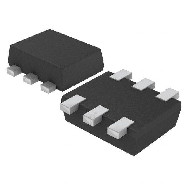
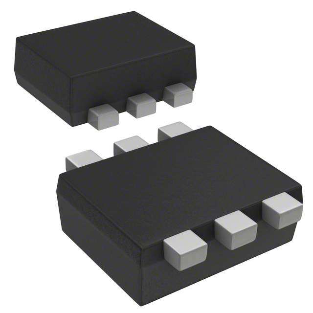
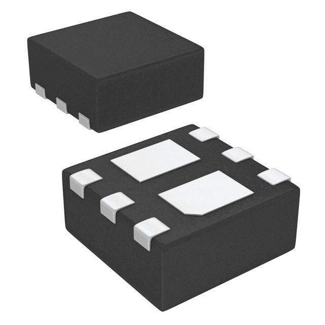
| 供应商器件封装 | SSMini6-F3-B |
| 其它名称 | FG6943010RDKR |
| 功率-最大值 | - |
| 包装 | Digi-Reel® |
| 商标 | Panasonic |
| 安装类型 | 表面贴装 |
| 安装风格 | SMD/SMT |
| 封装 | Reel |
| 封装/外壳 | SOT-563,SOT-666 |
| 封装/箱体 | SSMini-6-F3-B |
| 工厂包装数量 | 8000 |
| 晶体管极性 | N and P-Channel |
| 标准包装 | 1 |
| 漏源极电压(Vdss) | 30V |
| 电流-连续漏极(Id)(25°C时) | 100mA |
| 配置 | Dual |


- 商务部:美国ITC正式对集成电路等产品启动337调查
- 曝三星4nm工艺存在良率问题 高通将骁龙8 Gen1或转产台积电
- 太阳诱电将投资9.5亿元在常州建新厂生产MLCC 预计2023年完工
- 英特尔发布欧洲新工厂建设计划 深化IDM 2.0 战略
- 台积电先进制程称霸业界 有大客户加持明年业绩稳了
- 达到5530亿美元!SIA预计今年全球半导体销售额将创下新高
- 英特尔拟将自动驾驶子公司Mobileye上市 估值或超500亿美元
- 三星加码芯片和SET,合并消费电子和移动部门,撤换高东真等 CEO
- 三星电子宣布重大人事变动 还合并消费电子和移动部门
- 海关总署:前11个月进口集成电路产品价值2.52万亿元 增长14.8%


PDF Datasheet 数据手册内容提取
Doc No. TT4-EA-12659 Revision. 2 Product Standards MOS FET FG6943010R FG6943010R Silicon N-channel MOSFET(FET1) Silicon P-channel MOSFET(FET2) Unit : mm 1.6 0.2 0.13 6 5 4 For switching 26 .. 11 Features 1 2 3 Low drive voltage: 2.5 V drive (0.6) Halogen-free / RoHS compliant (0.5)(0.5) (EU RoHS / UL-94 V-0 / MSL:Level 1 compliant) 1.0 Marking Symbol V7 1. Source(FET1) 4. Source(FET2) 2. Gate(FET1) 5. Gate(FET2) 3. Drain(FET2) 6. Drain(FET1) Basic Part Number FJ330301 + FK330301 (Individual) Panasonic SSMini6-F3-B JEITA SC-107C Packaging Code SOT-666 Embossed type (Thermo-compression sealing) 8 000 pcs / reel (standard) Internal Connection (D1) (G2) (S2) 6 5 4 Absolute Maximum Ratings Ta = 25C Parameter Symbol Rating Unit FET1 Drain-source voltage VDS 30 V Gate-source voltage VGS 12 V FET1 Drain current ID 100 mA FET2 Pulse drain current IDp 200 mA Drain-source voltage VDS -30 V 1 2 3 Gate-source voltage VGS 12 V FET2 (S1) (G1) (D2) Drain current ID -100 mA Pulse drain current IDp -200 mA Pin name Total power dissipation PT 125 mW Channel temperature Tch 150 C 1. Source(FET1) 4. Source(FET2) Overall Operating ambient temperature Topr -40 to + 85 C 2. Gate(FET1) 5. Gate(FET2) Storage temperature Tstg -55 to +150 C 3. Drain(FET2) 6. Drain(FET1) Page 1 of 8 Established :2010-06-30 Revised :2013-10-10
Doc No. TT4-EA-12659 Revision. 2 Product Standards MOS FET FG6943010R Electrical Characteristics Ta = 25C 3C FET1 Parameter Symbol Conditions Min Typ Max Unit Drain-source breakdown voltage VDSS ID = 1 mA, VGS = 0 30 V Drain-source cutoff current IDSS VDS = 30 V, VGS = 0 1.0 A Gate-source cutoff current IGSS VGS = 10 V, VDS = 0 10 A Gate threshold voltage VTH ID = 1.0 A, VDS = 3.0 V 0.5 1.0 1.5 V RDS(on)1 ID = 10 mA, VGS = 2.5 V 3 6 Drain-source ON resistance RDS(on)2 ID = 10 mA, VGS = 4.0 V 2 3 Forward transfer admittance |Yfs| ID = 10 mA, VDS = 3.0 V 20 55 mS Input capacitance Ciss 12 pF Output capacitance Coss VDS = 3 V, VGS = 0, f = 1 MHz 7 pF Reverse transfer capacitance Crss 3 pF VDD = 3 V, VGS = 0 to 3 V Turn-on time *1 ton 100 ns ID = 10 mA VDD = 3 V, VGS = 3 to 0 V Turn-off time *1 toff 100 ns ID = 10 mA Note) 1. Measuring methods are based on JAPANESE INDUSTRIAL STANDARD JIS C 7030 Measuring methods for transistors. 2. *1 FET1 Turn-on and Turn-off test circuit VVDDDD==33VV IIDD==1100mmAA RRLL==330000ΩΩ DD VVoouutt VViinn VVGGSS==00~~33VV GG 5500ΩΩ SS Page 2 of 8 Established :2010-06-30 Revised :2013-10-10
Doc No. TT4-EA-12659 Revision. 2 Product Standards MOS FET FG6943010R Electrical Characteristics Ta = 25C 3C FET2 Parameter Symbol Conditions Min Typ Max Unit Drain-source breakdown voltage VDSS ID = -1mA, VGS = 0 -30 V Drain-source cutoff current IDSS VDS = -30 V, VGS = 0 -1.0 A Gate-source cutoff current IGSS VGS = 10 V, VDS = 0 10 A Gate threshold voltage VTH ID = -1.0 A, VDS = -3.0 V -0.5 -1.0 -1.5 V RDS(on)1 ID = -10 mA, VGS = -2.5 V 7 17 Drain-source ON resistance RDS(on)2 ID = -10 mA, VGS = -4.0 V 4 7 Forward transfer admittance |Yfs| ID = -10 mA, VDS = -3.0 V 20 40 mS Input capacitance Ciss 12 pF Output capacitance Coss VDS = -3 V, VGS = 0, f = 1 MHz 7 pF Reverse transfer capacitance Crss 3 pF VDD = -3 V, VGS = 0 to -3 V, Turn-on time *1 ton 100 ns ID = -10 mA VDD = -3 V, VGS = -3 to 0 V, Turn-off time *1 toff 100 ns ID = -10 mA Note) 1. Measuring methods are based on JAPANESE INDUSTRIAL STANDARD JIS C 7030 Measuring methods for transistors. 2. *1 FET2 Turn-on and Turn-off test circuit VVDDDD==--33VV IIDD==--1100mmAA RRLL==330000ΩΩ DD VVoouutt VViinn VVGGSS==00~~--33VV GG 5500ΩΩ SS Page 3 of 8 Established :2010-06-30 Revised :2013-10-10
Doc No. TT4-EA-12659 Revision. 2 Product Standards MOS FET FG6943010R Technical Data ( reference ) FET1(N-ch.) ID - VDS ID - VGS 0.1 1 0.1 D (A) D (A) urrent I 0.05 VGS = 4.0 V urrent I 0.01 Ta = 85 ℃ Drain C 2.5 V 2.0 V Drain c 0.001 25 ℃ 0.0001 -40 ℃ 1.5 V 0 0.00001 0 0.5 1 0 1 2 3 Drain-source Voltage VDS (V) Gate-source voltage VGS (V) VDS - VGS RDS(on) - ID 0.3 10000 e V) c DS ( stan 2.5 V V si e 0.2 10 mA Re) e Voltag ID = 20 mA n-State on) (m1000 VGS = 4.0 V ourc 0.1 e ODS( n-s urcR Drai 5 mA n-so ai 0 Dr 100 0 1 2 3 4 5 0.001 0.01 0.1 Gate-source Voltage VGS (V) Drain Current ID (A) Capacitance - VDS 100 F) p C ( e Ciss c 10 n a cit Coss a p a C Crss 1 0.1 1 10 100 Drain-source Voltage VDS (V) Page 4 of 8 Established :2010-06-30 Revised :2013-10-10
Doc No. TT4-EA-12659 Revision. 2 Product Standards MOS FET FG6943010R Technical Data ( reference ) FET1(N-ch.) Vth - Ta RDS(on) - Ta 2 3 ge ce VGS = 2.5V a n d Volt esista) 2 sholV) On-rn) ( 4.0 V ource TreVth ( 1.5 n-source RDS(o 1 ate-s Drai G 0 1 -50 0 50 100 150 -50 0 50 100 150 Temperature (℃) Temperature (℃) PD - Ta 0.2 W) D ( P n o ati p si 0.1 s Di er w o P al ot T 0 0 50 100 150 Temperature Ta (C) Rth - tsw Safe Operating Area 1000 10 W) C/ 1 IDp = 0.2 A esistance Rth ( 10100 n Current ID (A) 0.00.11 Ois pliemraitetiodn b iyn RthDisS a(orena) 1101100 msm msss R ai mal Dr 0.001 Ta = 25 ℃, DC Glass epoxy board (25.4×25.4×t0.8 mm) er coated with copper foil, Th 1 which has more than 300 mm2. 0.0001 0.001 0.01 0.1 1 10 100 1000 0.01 0.1 1 10 100 Pulse Width tsw (s) Drain-source Voltage VDS (V) Page 5 of 8 Established :2010-06-30 Revised :2013-10-10
Doc No. TT4-EA-12659 Revision. 2 Product Standards MOS FET FG6943010R Technical Data ( reference ) FET2(P-ch.) ID - VDS ID - VGS -0.1 -0.1 VGS = -4.0 V A) ent ID ( -0.05 -2.5 V nt ID (A)-0.05 Curr urre c n n Ta = 85 ℃ ai -1.5 V ai Dr Dr 25 ℃ -2.0 V -40 ℃ 0 0 0 -0.2 -0.4 -0.6 -0.8 -1 0 -1 -2 -3 Gate-source voltage VGS (V) Drain-source Voltage VDS (V) VDS - VGS RDS(on) - ID -0.5 1000000 e V) nc 1000 S ( -0.4 sta VD esi 100000 Drain-source Voltage ---000...321 -10 m-5A mA ID= -20 mA n-source On-state RRDS(on) () 111001000010000 V-2G.5S V = -4.0 V ai 0 Dr 0.1100 0 -1 -2 -3 -4 -5 -6 -0.001 -0.01 -0.1 Gate-source Voltage VGS (V) Drain Current ID (A) Capacitance - VDS 100 F) p C ( e Ciss c10 n a acit Coss p a C Crss 1 -0.1 -1 -10 -100 Drain-source Voltage VDS (V) Page 6 of 8 Established :2010-06-30 Revised :2013-10-10
Doc No. TT4-EA-12659 Revision. 2 Product Standards MOS FET FG6943010R Technical Data ( reference ) FET2(P-ch.) Vth - Ta RDS(on) - Ta -1 14 e e c 12 g n a a VGS = 2.5 V d Volt -1.5 esist) 10 sholV) On-rn) ( 8 source TheVth (-2-.25 n-source RDS(o 46 4.0 V Gate- Drai 2 0 -3 -50 0 50 100 150 -50 0 50 100 150 Temperature (℃) Temperature (℃) PD - Ta 0.2 W) D ( P n o ati p si 0.1 s Di er w o P al ot T 0 0 50 100 150 Temperature Ta (C) Rth -tsw Safe Operating Area 1000 -1.0E+01 W) C/ -1.0E+00 100 IDp = -0.2 A ce Rth ( nt ID (A) -1.0E-01 11 0m mss n 10 e sista Curr -1.0E-02 Operation in this area 110 s0 ms al Re 1 Drain Ta = 25 °C, is limited by RDS(on) DC m -1.0E-03 Glass epoxy board (25.4 × 25.4 × t0.8mm) er coated with copper foil, h which has more than 300mm2. T 0.1 -1.0E-04 0.001 0.01 0.1 1 10 100 1000 -0.01 -0.1 -1 -10 -100 Pulse Width tsw (s) Drain-source Voltage VDS (V) Page 7 of 8 Established :2010-06-30 Revised :2013-10-10
Doc No. TT4-EA-12659 Revision. 2 Product Standards MOS FET FG6943010R SSMini6-F3-B Unit: mm 1.60±0.05 +0.05 +0.05 0.13-0.02 0.20-0.02 6 5 4 5 5 0 0 . . 0 0 ± ± 0 0 2 6 . . 1 1 ) ° 1 2 3 5 ( 5 (0.5) (0.5) 0 . 0 ± 1.00±0.05 0 2 . 0 5 0 . 0 ± (5°) 5 5 . ) 0 7 2 . 0 ( 5 0 . 0 o t 0 Land Pattern (Reference) (Unit : mm 0.5 0.5 6 . 1 4 . 0 0.35 Page 8 of 8 Established :2010-06-30 Revised :2013-10-10
Request for your special attention and precautions in using the technical information and semiconductors described in this book (1) If anyof theproductsor technicalinformationdescribedinthisbook is tobe exported or provided to non-residents, the lawsandregulationsoftheexportingcountry,especially,thosewithregardtosecurityexportcontrol,mustbeobserved. (2)Thetechnicalinformationdescribedinthisbookisintendedonlytoshowthemaincharacteristicsandapplicationcircuit examples of the products. No license is granted in and to any intellectual property right or other right owned by Panasonic Corporation or any other company. Therefore, no responsibility is assumed by our company as to the infringement upon any such right owned by any other company which may arise as a result of the use of technical informationde-scribedinthisbook. (3) The products described in this book are intended to be used for general applications (such as office equipment, communicationsequipment,measuringinstrumentsandhouseholdappliances),orforspecificapplicationsasexpressly statedinthisbook. Please consult with our sales staff in advance for information on the following applications, moreover please exchange documentsseparatelyontermsofuseetc.:Specialapplications(suchasforin-vehicleequipment,airplanes,aerospace, automotive equipment, traffic signaling equipment, combustion equipment, medical equipment and safety devices) in which exceptional quality and reliability are required, or if the failure or malfunction of the products may directly jeopardizelifeorharmthehumanbody. Unlessexchangingdocumentsontermsofuseetc.inadvance,itistobeunderstoodthatourcompanyshallnotbeheld responsiblefor anydamageincurred asaresult of or inconnection with your usingthe productsdescribed inthisbook foranyspecialapplication. (4) The products and product specifications described in this book are subject to change without notice for modification and/orimprovement.Atthefinalstageofyourdesign,purchasing,oruseoftheproducts,therefore,askforthemostup- to-dateProductStandardsinadvancetomakesurethatthelatestspecificationssatisfyyourrequirements. (5) When designing your equipment, comply with the range of absolute maximum rating and the guaranteed operating conditions(operatingpowersupplyvoltageandoperatingenvironmentetc.).Especially,pleasebecarefulnottoexceed the range of absolute maximum rating on the transient state, such as power-on, power-off and mode-switching. Other- wise,wewillnotbeliableforanydefectwhichmayariselaterinyourequipment. Even when the products are used within the guaranteed values, take into the consideration of incidence of break down and failure mode, possible to occur to semiconductor products. Measures on the systems such as redundant design, arrestingthespreadoffireorpreventingglitcharerecommendedinordertopreventphysicalinjury,fire,socialdamages, forexample,byusingtheproducts. (6) Comply with the instructions for use in order to prevent breakdown and characteristics change due to external factors (ESD, EOS, thermal stress and mechanical stress) at the time of handling, mounting or at customer's process. We do notguaranteequalityfordisassembledproductsortheproductre-mountedafterremovingfromthemountingboard. Whenusingproductsforwhichdamp-proofpackingisrequired,satisfytheconditions,suchasshelflifeandtheelapsed timesincefirstopeningthepackages. (7) When reselling products described in this book to other companies without our permission and receiving any claim of requestfromtheresaledestination,pleaseunderstandthatcustomerswillbeartheburden. (8) This book may be not reprinted or reproduced whether wholly or partially, without the prior written permission of our company. No.010618