ICGOO在线商城 > 分立半导体产品 > 晶体管 - FET,MOSFET - 单 > FDA8440
 Datasheet下载
- 型号: FDA8440
- 制造商: Fairchild Semiconductor
- 库位|库存: xxxx|xxxx
- 要求:
| 数量阶梯 | 香港交货 | 国内含税 |
| +xxxx | $xxxx | ¥xxxx |
查看当月历史价格
查看今年历史价格
FDA8440产品简介:
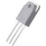
ICGOO电子元器件商城为您提供FDA8440由Fairchild Semiconductor设计生产,在icgoo商城现货销售,并且可以通过原厂、代理商等渠道进行代购。 FDA8440价格参考。Fairchild SemiconductorFDA8440封装/规格:晶体管 - FET,MOSFET - 单, 通孔 N 沟道 40V 30A(Ta),100A(Tc) 306W(Tc) TO-3PN。您可以下载FDA8440参考资料、Datasheet数据手册功能说明书,资料中有FDA8440 详细功能的应用电路图电压和使用方法及教程。
| 参数 | 数值 |
| 产品目录 | |
| ChannelMode | Enhancement |
| 描述 | MOSFET N-CH 40V 100A TO-3PNMOSFET 40V 100A 2.1mOhm N-Chan Power Trench |
| 产品分类 | FET - 单分离式半导体 |
| FET功能 | 逻辑电平门 |
| FET类型 | MOSFET N 通道,金属氧化物 |
| Id-ContinuousDrainCurrent | 30 A |
| Id-连续漏极电流 | 30 A |
| 品牌 | Fairchild Semiconductor |
| 产品手册 | |
| 产品图片 |
|
| rohs | 符合RoHS无铅 / 符合限制有害物质指令(RoHS)规范要求 |
| 产品系列 | 晶体管,MOSFET,Fairchild Semiconductor FDA8440PowerTrench® |
| 数据手册 | |
| 产品型号 | FDA8440 |
| PCN封装 | |
| PCN设计/规格 | |
| Pd-PowerDissipation | 306 W |
| Pd-功率耗散 | 306 W |
| RdsOn-Drain-SourceResistance | 2.1 mOhms |
| RdsOn-漏源导通电阻 | 2.1 mOhms |
| Vds-Drain-SourceBreakdownVoltage | 40 V |
| Vds-漏源极击穿电压 | 40 V |
| Vgs-Gate-SourceBreakdownVoltage | +/- 20 V |
| Vgs-栅源极击穿电压 | 20 V |
| 上升时间 | 130 ns |
| 下降时间 | 290 ns |
| 不同Id时的Vgs(th)(最大值) | 3V @ 250µA |
| 不同Vds时的输入电容(Ciss) | 24740pF @ 25V |
| 不同Vgs时的栅极电荷(Qg) | 450nC @ 10V |
| 不同 Id、Vgs时的 RdsOn(最大值) | 2.1 毫欧 @ 80A,10V |
| 产品目录页面 | |
| 产品种类 | MOSFET |
| 供应商器件封装 | TO-3PN |
| 典型关闭延迟时间 | 435 ns |
| 功率-最大值 | 306W |
| 包装 | 管件 |
| 单位重量 | 6.401 g |
| 商标 | Fairchild Semiconductor |
| 安装类型 | 通孔 |
| 安装风格 | Through Hole |
| 封装 | Tube |
| 封装/外壳 | TO-3P-3,SC-65-3 |
| 封装/箱体 | TO-3PN-3 |
| 工厂包装数量 | 30 |
| 晶体管极性 | N-Channel |
| 最大工作温度 | + 175 C |
| 最小工作温度 | - 55 C |
| 标准包装 | 30 |
| 漏源极电压(Vdss) | 40V |
| 电流-连续漏极(Id)(25°C时) | 30A (Ta), 100A (Tc) |
| 系列 | FDA8440 |
| 通道模式 | Enhancement |
| 配置 | Single |


PDF Datasheet 数据手册内容提取
Is Now Part of To learn more about ON Semiconductor, please visit our website at www.onsemi.com Please note: As part of the Fairchild Semiconductor integration, some of the Fairchild orderable part numbers will need to change in order to meet ON Semiconductor’s system requirements. Since the ON Semiconductor product management systems do not have the ability to manage part nomenclature that utilizes an underscore (_), the underscore (_) in the Fairchild part numbers will be changed to a dash (-). This document may contain device numbers with an underscore (_). Please check the ON Semiconductor website to verify the updated device numbers. The most current and up-to-date ordering information can be found at www.onsemi.com. Please email any questions regarding the system integration to Fairchild_questions@onsemi.com. ON Semiconductor and the ON Semiconductor logo are trademarks of Semiconductor Components Industries, LLC dba ON Semiconductor or its subsidiaries in the United States and/or other countries. ON Semiconductor owns the rights to a number of patents, trademarks, copyrights, trade secrets, and other intellectual property. A listing of ON Semiconductor’s product/patent coverage may be accessed at www.onsemi.com/site/pdf/Patent-Marking.pdf. ON Semiconductor reserves the right to make changes without further notice to any products herein. ON Semiconductor makes no warranty, representation or guarantee regarding the suitability of its products for any particular purpose, nor does ON Semiconductor assume any liability arising out of the application or use of any product or circuit, and specifically disclaims any and all liability, including without limitation special, consequential or incidental damages. Buyer is responsible for its products and applications using ON Semiconductor products, including compliance with all laws, regulations and safety requirements or standards, regardless of any support or applications information provided by ON Semiconductor. “Typical” parameters which may be provided in ON Semiconductor data sheets and/or specifications can and do vary in different applications and actual performance may vary over time. All operating parameters, including “Typicals” must be validated for each customer application by customer’s technical experts. ON Semiconductor does not convey any license under its patent rights nor the rights of others. ON Semiconductor products are not designed, intended, or authorized for use as a critical component in life support systems or any FDA Class 3 medical devices or medical devices with a same or similar classification in a foreign jurisdiction or any devices intended for implantation in the human body. Should Buyer purchase or use ON Semiconductor products for any such unintended or unauthorized application, Buyer shall indemnify and hold ON Semiconductor and its officers, employees, subsidiaries, affiliates, and distributors harmless against all claims, costs, damages, and expenses, and reasonable attorney fees arising out of, directly or indirectly, any claim of personal injury or death associated with such unintended or unauthorized use, even if such claim alleges that ON Semiconductor was negligent regarding the design or manufacture of the part. ON Semiconductor is an Equal Opportunity/Affirmative Action Employer. This literature is subject to all applicable copyright laws and is not for resale in any manner.
F D A 8 4 April 2014 4 0 N - C FDA8440 h a n ® N-Channel Logic Level PowerTrench MOSFET n e l 40 V, 100 A, 2.1 mΩ L o g Features Application i c L • RDS(on) = 1.46 mΩ (Typ.) @ VGS = 10 V, ID = 80 A • Power tools e v • Q = 345 nC (Typ.) @ V = 10 V G(tot) GS • Motor drives and Uninterruptible Power Supplies e • Low Miller Charge l • Synchronous Rectification P • Low Qrr Body Diode o • UIS Capability (Single Pulse and Repetitive Pulse) • Battery Protection Circuit w e • 160 A Guarantee for 2 sec r T • RoHS Compliant r e n c h ® D M O S F E T G G D TO-3PN S S MOSFET Maximum Ratings TC = 25oC unless otherwise noted. Symbol Parameter FDA8440 Unit V Drain to Source Voltage 40 V DSS V Gate to Source Voltage ±20 V GSS Drain Current - Continuous (T = 155oC) 100 A C ID - Continuous (TA = 25oC, VGS = 10 V, RθJA = 40oC/W ) 30 A - Pulsed 500 A E Single Pulsed Avalanche Energy (Note 1) 1682 mJ AS Power dissipation 306 W P D Derate above 25oC 2.04 W/oC T T Operating and Storage Temperature -55 to +175 oC J, STG Thermal Characteristics RθJC Thermal Resistance, Junction to Case, Max. 0.49 oC/W RθJA Thermal Resistance, Junction to Ambient, Max. (Note 2) 40 oC/W ©2007 Fairchild Semiconductor Corporation 1 www.fairchildsemi.com FDA8440 Rev. C1
F D Package Marking and Ordering Information A 8 4 Part Number Top Mark Package Packing Method Reel Size Tape Width Quantity 4 FDA8440 FDA8440 TO-3PN Tube N/A N/A 30 units 0 N Electrical Characteristics - TC = 25°C unless otherwise noted C h Symbol Parameter Conditions Min. Typ. Max. Unit a n Off Characteristics n e BVDSS Drain to Source Breakdown Voltage VGS = 0 V, ID = 250 μA 40 -- -- V l L V = 32 V -- -- 1 μA o DS g I Zero Gate Voltage Drain Current DSS VGS = 0 V TC = 150oC -- -- 250 μA ic L IGSS Gate to Body Leakage Current VGS = ±20 V -- -- ±100 nA e v On Characteristics e l VGS(th) Gate to Source Threshold Voltage VDS = VGS, ID = 250 μA 1 -- 3 V P o VGS = 4.5 V, ID = 80 A -- 1.56 2.2 w RDS(on) Static Drain-Source On-Resistance V = 10 V, I = 80 A -- 1.46 2.1 e GS D mΩ r T VTG S= =1 7150o VC, ID = 80 A, -- 2.82 4.1 re C n Dynamic Characteristics c h C Input Capacitance -- 18600 24740 pF ® iss M V = 25 V, V = 0 V, Coss Output Capacitance f =D S1 MHz GS -- 1840 2450 pF O C Reverse Transfer Capacitance -- 1400 2100 pF S rss F R Gate Resistance V = 0.5 V, f = 1 MHz -- 1.1 -- Ω E G GS T Q Total Gate Charge at 10V V = 0 V to 10 V -- 345 450 nC g(tot) GS Qg(2) Threshold Gate Charge VGS = 0 V to 2 V VDD = 20 V -- 32.5 -- nC Qgs Gate to Source Gate Charge ID = 80 A -- 49 -- nC Qgs2 Gate Charge Threshold to Plateau Ig = 1.0 mA -- 16.5 -- nC Q Gate to Drain “Miller” Charge -- 74 -- nC gd Switching Characteristics t Turn-On Time -- 175 360 ns ON t Turn-On Delay Time -- 43 95 ns d(on) V = 20 V,I = 80 A DD D tr Rise Time VGS = 10 V, RGEN = 7 Ω -- 130 275 ns t Turn-Off Delay Time -- 435 875 ns d(off) t Fall Time -- 290 590 ns f t Turn-Off Time -- 730 1470 ns OFF Drain-Source Diode Characteristics and Maximum Ratings I = 80 A -- -- 1.25 V V Source to Drain Diode Voltage SD SD I = 40 A -- -- 1.0 V SD t Reverse Recovery Time I = 75 A, dI /dt = 100 A/μs -- 59 -- ns rr SD SD Q Reverse Recovery Charge I = 75 A, dI /dt = 100 A/μs -- 77 -- nC RR SD SD NOTES: 1: Starting TJ = 25°C, L = 1 mH, IAS = 58 A, VDD = 36 V, VGS = 10 V. 2: Pulse width = 100 s. ©2007 Fairchild Semiconductor Corporation 2 www.fairchildsemi.com FDA8440 Rev. C1
F D Typical Performance Characteristics A 8 4 4 0 Figure 1. On-Region Characteristics Figure 2. Transfer Characteristics N 400 400 -C h a n 100 100 n e A] A] l n Current[ 10 V G S = 1 0753....0005 VVVV n Current[ 150oC -55oC Logic ai 3.0 V ai 10 L Dr 2.5 V Dr 25oC e ,D ,D v I I e l * Notes : * Notes : P 1 1. 250μs Pulse Test 1. VDS = 20V o 0.4 2. TC = 25oC 1 2. 250μs Pulse Test we 0.04 0.1 1 0 2 4 6 r VDS,Drain-Source Voltage[V] VGS,Gate-Source Voltage[V] Tr e n Figure 3. On-Resistance Variation vs. Figure 4. Body Diode Forward Voltage c h Drain Current and Gate Voltage Variation vs. Source Current ® and Temperatue M 1.60 1000 O S F ce VGS = 4.5V A] ET []ΩR m,DS(ON)Source On-Resistan11..5505 erse Drain Current [ 10100 150oC 25oC Drain- VGS = 10V I, RevS N1.o Vtes: = 0V GS 1.45 * Note : TJ = 25oC 2. 250μs Pulse Test 1 0 50 100 150 200 250 0.3 0.6 0.9 1.2 ID, Drain Current [A] VSD, Body Diode Forward Voltage [V] Figure 5. Capacitance Characteristics Figure 6. Gate Charge Characteristics 30000 10 Ciss = Cgs + Cgd (Cds = shorted) Coss = Cds + Cgd VDS = 25V 24000 Crss = Cgd e [V] 8 VVDDSS == 2105VV g F] Ciss olta s [p 18000 ce V 6 ce ur n o a * Note: S acit 12000 Coss 1. VGS = 0V ate- 4 p 2. f = 1MHz G Ca , S 6000 VG 2 Crss 0 0 * Note : ID = 80A 10-1 100 101 20 0 100 200 300 400 VDS, Drain-Source Voltage [V] Qg, Total Gate Charge [nC] ©2007 Fairchild Semiconductor Corporation 3 www.fairchildsemi.com FDA8440 Rev. C1
F D Typical Performance Characteristics (Continued) A 8 4 4 0 Figure 7. Breakdown Voltage Variation Figure 8. On-Resistance Variation N vs. Temperature vs. Temperature - C h 1.2 2.5 a n ge n BV, [Normalized]DSSDrain-Source Breakdown Volta 011...901 * N1o. VteGsS : = 0V r, [Normalized]DS(on)Drain-Source On-Resistance 0112....5050 * N1o. VteGsS : = 10V el Logic Level Powe 2. ID = 250μA 2. ID = 80A r 0.8 0.0 T -100 -50 0 50 100 150 200 -100 -50 0 50 100 150 200 r TJ, Junction Temperature [oC] TJ, Junction Temperature [oC] en c h Figure 9. Unclamped Inductive Switching Figure 10. Safe Operating Area ® Capability M O S 200 5000 F E 100 1000 T A) T( A] 100μs REN TJ = 25oC ent [ 100 UR urr C C ANCHE 10 TJ = 150oC , Drain D 10 Oisp Leirmaittieodn biny TRh DisS (Aonre)a 1ms AL I * Notes : 10ms AV 1 1. TC = 25oC I, AS 2. TJ = 175oC 100ms 3. Single Pulse 1 0.1 0.01 0.1 1 10 100 1000 10000 1 10 50 t , TIME IN A VALANCHE(ms) VDS, Drain-Sou rce Voltage [V] AV F i g u r e 1 1 . T r a nsient Thermal Response Curve 1 ] ZθJC 0.5 [e 0.1 0.2 s n po 0.1 PDM s 0.05 al Re 0.01 0.02 t1t2 m 0.01 * Notes : her Single pulse 1. ZθJC(t) = 0.49oC/W Max. T 2. Duty Factor, D=t1/t2 3. TJM - TC = PDM * ZθJC(t) 0.001 10-5 10-4 10-3 10-2 10-1 100 Rectangular Pulse Duration [sec] ©2007 Fairchild Semiconductor Corporation 4 www.fairchildsemi.com FDA8440 Rev. C1
F D A 8 4 4 0 N - C h a n n e l L o g i c L e v e l P o w e r T Figure 12. Gate Charge Test Circuit & Waveform re n c h ® M O S F E T Figure 13. Resistive Switching Test Circuit & Waveforms Figure 14. Unclamped Inductive Switching Test Circuit & Waveforms ©2007 Fairchild Semiconductor Corporation 5 www.fairchildsemi.com FDA8440 Rev. C1
F D A 8 4 4 0 N - C h a n n e l L o g i c L e v e l P o w e r T r e n c h ® M O S F E T Figure 15. Peak Diode Recovery dv/dt Test Circuit & Waveforms ©2007 Fairchild Semiconductor Corporation 6 www.fairchildsemi.com FDA8440 Rev. C1
F D Mechanical Dimensions A 8 4 4 0 N - C h a n n e l L o g i c L e v e l P o w e r T r e n c h ® M O S F E T Figure 16. TO3PN, 3-Lead, Plastic, EIAJ SC-65 Package drawings are provided as a service to customers considering Fairchild components. Drawings may change in any manner without notice. Please note the revision and/or date on the drawing and contact a Fairchild Semiconductor representative to verify or obtain the most recent revision. Package specifications do not expand the terms of Fairchild’s worldwide terms and conditions, specif- ically the warranty therein, which covers Fairchild products. Always visit Fairchild Semiconductor’s online packaging area for the most recent package drawings: http://www.fairchildsemi.com/package/packageDetails.html?id=PN_TT3PN-003 ©2007 Fairchild Semiconductor Corporation 7 www.fairchildsemi.com FDA8440 Rev. C1
F D A 8 4 4 0 N - C TRADEMARKS h The following includes registered and unregistered trademarks and service marks, owned by Fairchild Semiconductor and/or its global subsidiaries, and is not a n intended to be an exhaustive list of all such trademarks. n AABBXiuctSci-ludCiC PAit™o PNw®oe*wr™™ FFGGR-lrPoeFbFeEanSTlB ™P®riodwgeer™ ResourceSM PPoowwtm®eerrTXrSe™nch® TTiinnyyBBouocks®t®®* el Log CorePLUS™ Green FPS™ Programmable Active Droop™ CCoRrOePSOSVWOELRT™™ GGrmeaexn™ FPS™ e-Series™ QQFSE™T® TTTiIinnNyyYCLOoagPlciTc™®O™ ic L CTL™ GTO™ Quiet Series™ e TinyPower™ Current Transfer Logic™ IntelliMAX™ RapidConfigure™ v DEUXPEED® ISOPLANAR™ ™ TinyPWM™ e TinyWire™ l Dual Cool™ Marking Small Speakers Sound Louder EcoSPARK® and Better™ Saving our world, 1mW/W/kW at a time™ TranSiC™ P TriFault Detect™ o EfficentMax™ MegaBuck™ SignalWise™ TRUECURRENT®* w ESBC™ MICROCOUPLER™ SmartMax™ μSerDes™ e ® MicroFET™ SMART START™ r MicroPak™ Solutions for Your Success™ T Fairchild® MicroPak2™ SPM® re Fairchild Semiconductor® MillerDrive™ STEALTH™ UHC® n FACT Quiet Series™ MotionMax™ SuperFET® Ultra FRFET™ c FACT® mWSaver® SuperSOT™-3 UniFET™ h FAST® OptoHiT™ SuperSOT™-6 VCX™ ® FastvCore™ OPTOLOGIC® SuperSOT™-8 VisualMax™ M FETBench™ OPTOPLANAR® SupreMOS® VoltagePlus™ O FPS™ SyncFET™ XS™ S Sync-Lock™ ? ? ™ F E T *Trademarks of System General Corporation, used under license by Fairchild Semiconductor. DISCLAIMER FAIRCHILD SEMICONDUCTOR RESERVES THE RIGHT TO MAKE CHANGES WITHOUT FURTHER NOTICE TO ANY PRODUCTS HEREIN TO IMPROVE RELIABILITY, FUNCTION, OR DESIGN. FAIRCHILD DOES NOT ASSUME ANY LIABILITY ARISING OUT OF THE APPLICATION OR USE OF ANY PRODUCT OR CIRCUIT DESCRIBED HEREIN; NEITHER DOES IT CONVEY ANY LICENSE UNDER ITS PATENT RIGHTS, NOR THE RIGHTS OF OTHERS. THESE SPECIFICATIONS DO NOT EXPAND THE TERMS OF FAIRCHILD’S WORLDWIDE TERMS AND CONDITIONS, SPECIFICALLY THE WARRANTY THEREIN, WHICH COVERS THESE PRODUCTS. LIFE SUPPORT POLICY FAIRCHILD’S PRODUCTS ARE NOT AUTHORIZED FOR USE AS CRITICAL COMPONENTS IN LIFE SUPPORT DEVICES OR SYSTEMS WITHOUT THE EXPRESS WRITTEN APPROVAL OF FAIRCHILD SEMICONDUCTOR CORPORATION. As used here in: 1. Life support devices or systems are devices or systems which, (a) are 2. A critical component in any component of a life support, device, or intended for surgical implant into the body or (b) support or sustain life, system whose failure to perform can be reasonably expected to cause and (c) whose failure to perform when properly used in accordance with the failure of the life support device or system, or to affect its safety or instructions for use provided in the labeling, can be reasonably effectiveness. expected to result in a significant injury of the user. ANTI-COUNTERFEITING POLICY Fairchild Semiconductor Corporation’s Anti-Counterfeiting Policy. Fairchild’s Anti-Counterfeiting Policy is also stated on our external website, www.Fairchildsemi.com, under Sales Support. Counterfeiting of semiconductor parts is a growing problem in the industry. All manufactures of semiconductor products are experiencing counterfeiting of their parts. Customers who inadvertently purchase counterfeit parts experience many problems such as loss of brand reputation, substandard performance, failed application, and increased cost of production and manufacturing delays. Fairchild is taking strong measures to protect ourselves and our customers from the proliferation of counterfeit parts. Fairchild strongly encourages customers to purchase Fairchild parts either directly from Fairchild or from Authorized Fairchild Distributors who are listed by country on our web page cited above. Products customers buy either from Fairchild directly or from Authorized Fairchild Distributors are genuine parts, have full traceability, meet Fairchild’s quality standards for handing and storage and provide access to Fairchild’s full range of up-to-date technical and product information. Fairchild and our Authorized Distributors will stand behind all warranties and will appropriately address and warranty issues that may arise. Fairchild will not provide any warranty coverage or other assistance for parts bought from Unauthorized Sources. Fairchild is committed to combat this global problem and encourage our customers to do their part in stopping this practice by buying direct or from authorized distributors. PRODUCT STATUS DEFINITIONS Definition of Terms Datasheet Identification Product Status Definition Datasheet contains the design specifications for product development. Specifications Advance Information Formative / In Design may change in any manner without notice. Datasheet contains preliminary data; supplementary data will be published at a later Preliminary First Production date. Fairchild Semiconductor reserves the right to make changes at any time without notice to improve design. Datasheet contains final specifications. Fairchild Semiconductor reserves the right to No Identification Needed Full Production make changes at any time without notice to improve the design. Datasheet contains specifications on a product that is discontinued by Fairchild Obsolete Not In Production Semiconductor. The datasheet is for reference information only. Rev. I68 ©2007 Fairchild Semiconductor Corporation 8 www.fairchildsemi.com FDA8440 Rev. C1
ON Semiconductor and are trademarks of Semiconductor Components Industries, LLC dba ON Semiconductor or its subsidiaries in the United States and/or other countries. ON Semiconductor owns the rights to a number of patents, trademarks, copyrights, trade secrets, and other intellectual property. A listing of ON Semiconductor’s product/patent coverage may be accessed at www.onsemi.com/site/pdf/Patent−Marking.pdf. ON Semiconductor reserves the right to make changes without further notice to any products herein. ON Semiconductor makes no warranty, representation or guarantee regarding the suitability of its products for any particular purpose, nor does ON Semiconductor assume any liability arising out of the application or use of any product or circuit, and specifically disclaims any and all liability, including without limitation special, consequential or incidental damages. Buyer is responsible for its products and applications using ON Semiconductor products, including compliance with all laws, regulations and safety requirements or standards, regardless of any support or applications information provided by ON Semiconductor. “Typical” parameters which may be provided in ON Semiconductor data sheets and/or specifications can and do vary in different applications and actual performance may vary over time. All operating parameters, including “Typicals” must be validated for each customer application by customer’s technical experts. ON Semiconductor does not convey any license under its patent rights nor the rights of others. ON Semiconductor products are not designed, intended, or authorized for use as a critical component in life support systems or any FDA Class 3 medical devices or medical devices with a same or similar classification in a foreign jurisdiction or any devices intended for implantation in the human body. Should Buyer purchase or use ON Semiconductor products for any such unintended or unauthorized application, Buyer shall indemnify and hold ON Semiconductor and its officers, employees, subsidiaries, affiliates, and distributors harmless against all claims, costs, damages, and expenses, and reasonable attorney fees arising out of, directly or indirectly, any claim of personal injury or death associated with such unintended or unauthorized use, even if such claim alleges that ON Semiconductor was negligent regarding the design or manufacture of the part. ON Semiconductor is an Equal Opportunity/Affirmative Action Employer. This literature is subject to all applicable copyright laws and is not for resale in any manner. PUBLICATION ORDERING INFORMATION LITERATURE FULFILLMENT: N. American Technical Support: 800−282−9855 Toll Free ON Semiconductor Website: www.onsemi.com Literature Distribution Center for ON Semiconductor USA/Canada 19521 E. 32nd Pkwy, Aurora, Colorado 80011 USA Europe, Middle East and Africa Technical Support: Order Literature: http://www.onsemi.com/orderlit Phone: 303−675−2175 or 800−344−3860 Toll Free USA/Canada Phone: 421 33 790 2910 Fax: 303−675−2176 or 800−344−3867 Toll Free USA/Canada Japan Customer Focus Center For additional information, please contact your local Email: orderlit@onsemi.com Phone: 81−3−5817−1050 Sales Representative © Semiconductor Components Industries, LLC www.onsemi.com www.onsemi.com 1
Mouser Electronics Authorized Distributor Click to View Pricing, Inventory, Delivery & Lifecycle Information: O N Semiconductor: FDA8440