ICGOO在线商城 > 分立半导体产品 > 晶体管 - FET,MOSFET - 单 > FCP7N60
 Datasheet下载
- 型号: FCP7N60
- 制造商: Fairchild Semiconductor
- 库位|库存: xxxx|xxxx
- 要求:
| 数量阶梯 | 香港交货 | 国内含税 |
| +xxxx | $xxxx | ¥xxxx |
查看当月历史价格
查看今年历史价格
FCP7N60产品简介:
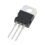
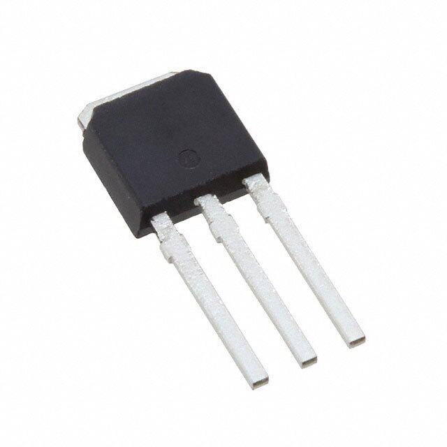
ICGOO电子元器件商城为您提供FCP7N60由Fairchild Semiconductor设计生产,在icgoo商城现货销售,并且可以通过原厂、代理商等渠道进行代购。 FCP7N60价格参考。Fairchild SemiconductorFCP7N60封装/规格:晶体管 - FET,MOSFET - 单, 通孔 N 沟道 600V 7A(Tc) 83W(Tc) TO-220-3。您可以下载FCP7N60参考资料、Datasheet数据手册功能说明书,资料中有FCP7N60 详细功能的应用电路图电压和使用方法及教程。
| 参数 | 数值 |
| 产品目录 | |
| ChannelMode | Enhancement |
| 描述 | MOSFET N-CH 600V 7A TO-220MOSFET 600V N-Channel SuperFET |
| 产品分类 | FET - 单分离式半导体 |
| FET功能 | 标准 |
| FET类型 | MOSFET N 通道,金属氧化物 |
| Id-ContinuousDrainCurrent | 7 A |
| Id-连续漏极电流 | 7 A |
| 品牌 | Fairchild Semiconductor |
| 产品手册 | |
| 产品图片 |
|
| rohs | 符合RoHS无铅 / 符合限制有害物质指令(RoHS)规范要求 |
| 产品系列 | 晶体管,MOSFET,Fairchild Semiconductor FCP7N60SuperFET™ |
| 数据手册 | |
| 产品型号 | FCP7N60 |
| PCN组件/产地 | |
| Pd-PowerDissipation | 83 W |
| Pd-功率耗散 | 83 W |
| RdsOn-Drain-SourceResistance | 530 mOhms |
| RdsOn-漏源导通电阻 | 530 mOhms |
| Vds-Drain-SourceBreakdownVoltage | 600 V |
| Vds-漏源极击穿电压 | 600 V |
| Vgs-Gate-SourceBreakdownVoltage | +/- 30 V |
| Vgs-栅源极击穿电压 | 30 V |
| 上升时间 | 55 ns |
| 下降时间 | 32 ns |
| 不同Id时的Vgs(th)(最大值) | 5V @ 250µA |
| 不同Vds时的输入电容(Ciss) | 920pF @ 25V |
| 不同Vgs时的栅极电荷(Qg) | 30nC @ 10V |
| 不同 Id、Vgs时的 RdsOn(最大值) | 600 毫欧 @ 3.5A,10V |
| 产品培训模块 | http://www.digikey.cn/PTM/IndividualPTM.page?site=cn&lang=zhs&ptm=356 |
| 产品种类 | MOSFET |
| 供应商器件封装 | TO-220 |
| 其它名称 | FCP7N60_NL |
| 典型关闭延迟时间 | 75 ns |
| 功率-最大值 | 83W |
| 包装 | 管件 |
| 单位重量 | 1.800 g |
| 商标 | Fairchild Semiconductor |
| 安装类型 | 通孔 |
| 安装风格 | Through Hole |
| 封装 | Tube |
| 封装/外壳 | TO-220-3 |
| 封装/箱体 | TO-220-3 |
| 工厂包装数量 | 50 |
| 晶体管极性 | N-Channel |
| 最大工作温度 | + 150 C |
| 最小工作温度 | - 55 C |
| 标准包装 | 50 |
| 正向跨导-最小值 | 6 S |
| 漏源极电压(Vdss) | 600V |
| 电流-连续漏极(Id)(25°C时) | 7A (Tc) |
| 系列 | FCP7N60 |
| 通道模式 | Enhancement |
| 配置 | Single |


PDF Datasheet 数据手册内容提取
Is Now Part of To learn more about ON Semiconductor, please visit our website at www.onsemi.com Please note: As part of the Fairchild Semiconductor integration, some of the Fairchild orderable part numbers will need to change in order to meet ON Semiconductor’s system requirements. Since the ON Semiconductor product management systems do not have the ability to manage part nomenclature that utilizes an underscore (_), the underscore (_) in the Fairchild part numbers will be changed to a dash (-). This document may contain device numbers with an underscore (_). Please check the ON Semiconductor website to verify the updated device numbers. The most current and up-to-date ordering information can be found at www.onsemi.com. Please email any questions regarding the system integration to Fairchild_questions@onsemi.com. ON Semiconductor and the ON Semiconductor logo are trademarks of Semiconductor Components Industries, LLC dba ON Semiconductor or its subsidiaries in the United States and/or other countries. ON Semiconductor owns the rights to a number of patents, trademarks, copyrights, trade secrets, and other intellectual property. A listing of ON Semiconductor’s product/patent coverage may be accessed at www.onsemi.com/site/pdf/Patent-Marking.pdf. ON Semiconductor reserves the right to make changes without further notice to any products herein. ON Semiconductor makes no warranty, representation or guarantee regarding the suitability of its products for any particular purpose, nor does ON Semiconductor assume any liability arising out of the application or use of any product or circuit, and specifically disclaims any and all liability, including without limitation special, consequential or incidental damages. Buyer is responsible for its products and applications using ON Semiconductor products, including compliance with all laws, regulations and safety requirements or standards, regardless of any support or applications information provided by ON Semiconductor. “Typical” parameters which may be provided in ON Semiconductor data sheets and/or specifications can and do vary in different applications and actual performance may vary over time. All operating parameters, including “Typicals” must be validated for each customer application by customer’s technical experts. ON Semiconductor does not convey any license under its patent rights nor the rights of others. ON Semiconductor products are not designed, intended, or authorized for use as a critical component in life support systems or any FDA Class 3 medical devices or medical devices with a same or similar classification in a foreign jurisdiction or any devices intended for implantation in the human body. Should Buyer purchase or use ON Semiconductor products for any such unintended or unauthorized application, Buyer shall indemnify and hold ON Semiconductor and its officers, employees, subsidiaries, affiliates, and distributors harmless against all claims, costs, damages, and expenses, and reasonable attorney fees arising out of, directly or indirectly, any claim of personal injury or death associated with such unintended or unauthorized use, even if such claim alleges that ON Semiconductor was negligent regarding the design or manufacture of the part. ON Semiconductor is an Equal Opportunity/Affirmative Action Employer. This literature is subject to all applicable copyright laws and is not for resale in any manner.
F C P 7 N November 2013 6 0 / FCP7N60 / FCPF7N60 F C ® P N-Channel SuperFET MOSFET F 7 600 V, 7 A, 600 mΩ N 6 0 Features Description — • 650 V @ T = 150oC SuperFET® MOSFET is Fairchild Semiconductor’s first genera- N J - • Typ. R = 530 mΩ tion of high voltage super-junction (SJ) MOSFET family that is C DS(on) h utilizing charge balance technology for outstanding low on- • Ultra Low Gate Charge (Typ. Q = 23 nC) a g resistance and lower gate charge performance. This technology n • Low Effective Output Capacitance (Typ. Coss(eff.) = 60 pF) is tailored to minimize conduction loss, provide superior switch- n • 100% Avalanche Tested ing performance, dv/dt rate and higher avalanche energy. Con- el • RoHS Compliant sequently, SuperFET MOSFET is very suitable for the switching S u power applications such as PFC, server/telecom power, FPD Application p TV power, ATX power and industrial power applications. e r • LCD/LED/PDP TV F E • Solar Inverter T • AC-DC Power Supply ® M D O S F E T D G G D S TO-220 GDS TO-220F G S TO-220F Y-formed S Absolute Maximum Ratings TC = 25oC unless otherwise noted. FCPF7N60 / Symbol Parameter FCP7N60 Unit FCPF7N60YDTU V Drain-Source Voltage 600 V DSS I Drain Current - Continuous (T = 25°C) 7 7* A D C - Continuous (T = 100°C) 4.4 4.4* A C IDM Drain Current - Pulsed (Note 1) 21 21* A V Gate-Source voltage ± 30 V GSS E Single Pulsed Avalanche Energy (Note 2) 230 mJ AS I Avalanche Current (Note 1) 7 A AR E Repetitive Avalanche Energy (Note 1) 8.3 mJ AR dv/dt Peak Diode Recovery dv/dt (Note 3) 4.5 V/ns P Power Dissipation (T = 25°C) 83 31 W D C - Derate Above 25°C 0.67 0.25 W/°C T T Operating and Storage Temperature Range -55 to +150 °C J, STG T Maximum Lead Temperature for Soldering, L 300 °C 1/8” from Case for 5 Seconds *Drain current limited by maximum junction temperature. Thermal Characteristics FCPF7N60 / Symbol Parameter FCP7N60 Unit FCPF7N60YDTU RθJC Thermal Resistance, Junction-to-Case, Max. 1.5 4.0 °C/W RθJA Thermal Resistance, Junction-to-Ambient, Max. 62.5 62.5 ©2005 Fairchild Semiconductor Corporation 1 www.fairchildsemi.com FCP7N60 / FCPF7N60 Rev. C1
F C Package Marking and Ordering Information P 7 N Part Number Top Mark Package Packing Method Reel Size Tape Width Quantity 6 FCP7N60 FCP7N60 TO220 Tube N/A N/A 50 units 0 / FCPF7N60 FCPF7N60 TO220F Tube N/A N/A 50 units F TO-220F C FCPF7N60YDTU FCPF7N60 (Y-formed) Tube N/A N/A 50 units P F 7 Electrical Characteristics N T = 25°C unless otherwise noted. C 6 0 Symbol Parameter Conditions Min. Typ. Max. Unit — Off Characteristics N BVDSS Drain-Source Breakdown Voltage VGS = 0 V, ID = 250 μA, TJ = 25°C 600 -- -- V -C V = 0 V, I = 250 μA, T = 150°C -- 650 -- V h GS D J a ΔBV Breakdown Voltage Temperature n / ΔTDSS Coefficient ID = 250 μA, Referenced to 25°C -- 0.6 -- V/°C n J e l BV Drain-Source Avalanche Breakdown DS V = 0 V, I = 7 A -- 700 -- V S Voltage GS D u p IDSS Zero Gate Voltage Drain Current VDS = 600 V, VGS = 0 V -- -- 1 μA e V = 480 V, T = 125°C -- -- 10 μA r DS C F E I Gate-Body Leakage Current, Forward V = 30 V, V = 0 V -- -- 100 nA GSSF GS DS T I Gate-Body Leakage Current, Reverse V = -30 V, V = 0 V -- -- -100 nA ® GSSR GS DS M On Characteristics O V Gate Threshold Voltage V = V , I = 250 μA 3.0 -- 5.0 V S GS(th) DS GS D F RDS(on) Static Drain-Source V = 10 V, I = 3.5 A -- 0.53 0.6 Ω E On-Resistance GS D T g Forward Transconductance V = 40 V, I = 3.5 A -- 6 -- S FS DS D Dynamic Characteristics C Input Capacitance V = 25 V, V = 0 V, -- 710 920 pF iss DS GS f = 1 MHz C Output Capacitance -- 380 500 pF oss C Reverse Transfer Capacitance -- 34 -- pF rss C Output Capacitance V = 480 V, V = 0 V, f = 1 MHz -- 22 29 pF oss DS GS C Effective Output Capacitance V = 0 V to 400 V, V = 0 V -- 60 -- pF oss(eff.) DS GS Switching Characteristics t Turn-On Delay Time V = 300 V, I = 7 A, -- 35 80 ns d(on) DD D V = 10 V, R = 25 Ω t Turn-On Rise Time GS G -- 55 120 ns r t Turn-Off Delay Time -- 75 160 ns d(off) t Turn-Off Fall Time (Note 4) -- 32 75 ns f Q Total Gate Charge V = 480 V, I = 7 A, -- 23 30 nC g DS D V = 10 V Q Gate-Source Charge GS -- 4.2 5.5 nC gs Q Gate-Drain Charge (Note 4) -- 11.5 -- nC gd Drain-Source Diode Characteristics and Maximum Ratings I Maximum Continuous Drain-Source Diode Forward Current -- -- 7 A S I Maximum Pulsed Drain-Source Diode Forward Current -- -- 21 A SM V Drain-Source Diode Forward Voltage V = 0 V, I = 7 A -- -- 1.4 V SD GS S t Reverse Recovery Time V = 0 V, I = 7 A, -- 360 -- ns rr GS S Q Reverse Recovery Charge dIF/dt =100 A/μs -- 4.5 -- μC rr Notes: 1. Repetitive rating: pulse-width limited by maximum junction temperature. 2. IAS = 3.5 A, VDD = 50 V, RG = 25 Ω, starting TJ = 25°C. 3. ISD ≤ 7 A, di/dt ≤ 200 A/μs, VDD ≤ BVDSS, starting TJ = 25°C. 4. Essentially independent of operating temperature typical characteristics. ©2005 Fairchild Semiconductor Corporation 2 www.fairchildsemi.com FCP7N60 / FCPF7N60 Rev. C1
F C Typical Performance Characteristics P 7 N 6 0 Figure 1. On-Region Characteristics Figure 2. Transfer Characteristics / F C V P GS Top : 15.0 V F 10.0 V 7 8.0 V I, Drain Current [A]D111000-101 B o t t o m : 5766....5050 VVVV N 12o..t e2Ts5C 0:=μ s2 5P°uClse Test I , Drain Current [A]D 110001 25°1C50°C -55°C N 12o..t eV25DS0 μ=s 4 P0uVlse Test N60 — N-Chann e 10-1 100 101 10-12 4 6 8 10 l S VDS, Drain-Source Voltage [V] VGS , Gate-Source Voltage [V] u p e r Figure 3. On-Resistance Variation vs. Figure 4. Body Diode Forward Voltage F E Drain Current and Gate Voltage Variation vs. Source Current T and Temperatue ® M O 2.0 S ΩR [],DS(ON)Drain-Source On-Resistance00011111........46802468 VGS = 10V VGS = 20V I , Reverse Drain Current [A]DR 110001 150°C 25°C N 1o.t eVs : = 0V FET 0.2 Note : T = 25°C 2. 25G0Sμs Pulse Test J 0.0 10-1 0 5 10 15 20 0.2 0.4 0.6 0.8 1.0 1.2 1.4 1.6 I, Drain Current [A] V , Source-Drain Voltage [V] D SD Figure 5. Capacitance Characteristics Figure 6. Gate Charge Characteristics 3000 12 Ciss = Cgs + Cgd (Cds = shorted) V = 100V C = C + C DS Corssss = Cgdds gd e [V] 10 VDVS D=S 4=0 205V0V nce [pF] 2000 Coss ce Voltag 68 Capacita 1000 Ciss N 12o..t eVf s=G S :1 = M 0H Vz ate-Sour 4 G Crss , GS 2 V Note : I = 7A D 0 0 10-1 100 101 0 5 10 15 20 25 V , Drain-Source Voltage [V] Q, Total Gate Charge [nC] DS G ©2005 Fairchild Semiconductor Corporation 3 www.fairchildsemi.com FCP7N60 / FCPF7N60 Rev. C1
F C Typical Performance Characteristics P (Continued) 7 N 6 0 Figure 7. Breakdown Voltage Variation Figure 8. On-Resistance Variation / vs. Temperature vs. Temperature F C P 1.2 3.0 F e 7 BV, (Normalized)DSSSource Breakdown Voltag011...901 N 1o.t eVs : = 0 V R, (Normalized)DS(ON)ain-Source On-Resistance1122....0505 N60 — N-Chan Drain- 2. IDG =S 250μA Dr0.5 N 12o..t eVIDsG =S: =3 .150 A V nel 0.8 0.0 S -100 -50 0 50 100 150 200 -100 -50 0 50 100 150 200 u T, Junction Temperature [°C] T, Junction Temperature [°C] p J J e r F E T Figure 9-1. Maximum Safe Operating Area Figure 9-2. Maximum Safe Operating Area ® for FCP7N60 for FCPF7N60 M O S 102 Operation in This Area 102 Operation in This Area F is Limited by R DS(on) is Limited by R DS(on) E T ent [A] 101 10 m1s ms100 us ent [A] 101 10 m1s ms100 us n Curr 100 DC n Curr 100 DC100 ms ai ai Dr Dr I, D10-1 N 1o.t eTsC := 25°C I, D10-1 N 1o.t eTsC := 25°C 2. T = 150°C 2. T = 150°C J J 3. Single Pulse 3. Single Pulse 10-2 10-2 100 101 102 103 100 101 102 103 V , Drain-Source Voltage [V] V , Drain-Source Voltage [V] DS DS Figure 10. Maximum Drain Current vs. Case Temperature 10.0 7.5 A] nt [ e Curr 5.0 n ai Dr I, D 2.5 0.0 25 50 75 100 125 150 T, Case Temperature [?] C ©2005 Fairchild Semiconductor Corporation 4 www.fairchildsemi.com FCP7N60 / FCPF7N60 Rev. C1
F C Typical Performance Characteristics P (Continued) 7 N 6 0 Figure 11-1. Transient Thermal Response Curve for FCP7N60 / F C P F oZ(t), Thermal Response [C/W] θJCZ(t), Thermal ResponseθJC 111000--210 00D000..0.0..=0212105.5 single pulse P N D123oM...t eZDTsθJuJM C:t y(-t )TF =Cta1 c=1tt2 o.P5r°D, CMD /*=W Zt1 θ/MJtC2(atx). 7N60 — N-Channe l S 10-5 10-4 10-3 10-2 10-1 100 101 u t , Square Wave Pulse Duration [sec] p 1 e r F E T Figure 11-2. Transient Thermal Response Curve for FCPF7N60 ® M O S F W] D=0.5 ET C/ omal Response [ermal Response 1100-10 0000....001225 N 123o...t eZDTsθJuJM C:t y(-t )TF 4Ca .c=0t °oPCrD,/ MWD *= MZt1θ/aJtC2x(.t) Z(t), TherZ(t), ThθJCθJC 10-2 0.01 single pulse PDM t1t2 10-5 10-4 10-3 10-2 10-1 100 101 t , Square Wave Pulse Duration [sec] 1 ©2005 Fairchild Semiconductor Corporation 5 www.fairchildsemi.com FCP7N60 / FCPF7N60 Rev. C1
F C P 7 N 6 0 / F C P F VV 7 SSaammee TTyyppee GGSS N 6 5500KKΩΩ aass DDUUTT QQ 0 gg 1122VV 220000nnFF 1100VV — 330000nnFF N VV VV DDSS - GGSS QQ QQ C ggss ggdd h a n DDUUTT n e IG = co33nmmsAAt. l S u p CChhaarrggee e r F Figure 12. Gate Charge Test Circuit & Waveform E T ® M O S F VVDDSS RRLL VVDDSS 9900%% ET VVGGSS VVDDDD RR GG 1100%% VV V1100GVVS DDUUTT GGSS tt tt tt dd((oonn)) rr dd((ooffff)) tt ff tt tt oonn ooffff Figure 13. Resistive Switching Test Circuit & Waveforms BBVV LLL 1111 DDSSSS EEE === ---------------- LLLIII 222 ---------------------------------------- VVDDSS AAASSS 2222 AAASSS BBVV --VV DDSSSS DDDD BBVV III DDSSSS DDD II AASS RR GG VVDDDD IIDD ((tt)) VV11G00GVVSS DDUUTT VVDDDD VVDDSS ((tt)) tt pp tt TTiimmee pp Figure 14. Unclamped Inductive Switching Test Circuit & Waveforms ©2005 Fairchild Semiconductor Corporation 6 www.fairchildsemi.com FCP7N60 / FCPF7N60 Rev. C1
F C P 7 N 6 0 / F C P DDUUTT ++ F 7 N 6 VV DDSS 0 — __ N - C h IISSDD a n LLL n e l S DDrriivveerr u p RR e GG SSaammee TTyyppee rF aass DDUUTT VVDDDD E T ® VV GGSS ••ddvv//ddttccoonnttrroolllleedd bbyy RR M GG ••II ccoonnttrroolllleedd bbyy ppuullssee ppeerriioodd O SSDD S F E T GGGaaattteee PPPuuulllssseee WWWiiidddttthhh VVGGSS DDD ===------GGG------aaa------ttt---eee------ PPP------uuu------lll---sss---eee------ ---PPP------eee------rrr---iiiooo------ddd--- 1100VV (( DDrriivveerr )) II ,, BBooddyy DDiiooddee FFoorrwwaarrdd CCuurrrreenntt FFMM II SSDD (( DDUUTT )) ddii//ddtt II RRMM BBooddyy DDiiooddee RReevveerrssee CCuurrrreenntt VV DDSS (( DDUUTT )) BBooddyy DDiiooddee RReeccoovveerryyddvv//ddtt VV VV SSDD DDDD BBooddyy DDiiooddee FFoorrwwaarrdd VVoollttaaggee DDrroopp Figure 15. Peak Diode Recovery dv/dt Test Circuit & Waveforms ©2005 Fairchild Semiconductor Corporation 7 www.fairchildsemi.com FCP7N60 / FCPF7N60 Rev. C1
10.36 2.66 A B B 9.96 2.42 3.28 3.40 7.00 3.08 0.70 3.20 6.88 6.48 1 X 45° 16.07 B 15.67 16.00 15.60 R0.30 2.96 1 3 R0.30 2.56 1.47 1.24 10.45 B 10.00 2.14 9.45 B 9.00 0.90 0.70 0.50 M A 0.60 B 0.45 B 4.00 MIN 2.54 2.54 6.00 B 4.00 4.90 B 4.50 NOTES: A. EXCEPT WHERE NOTED CONFORMS TO EIAJ SC91A. B DOES NOT COMPLY EIAJ STD. VALUE. C. ALL DIMENSIONS ARE IN MILLIMETERS. D. DIMENSIONS ARE EXCLUSIVE OF BURRS, MOLD FLASH AND TIE BAR PROTRUSIONS. E. DIMENSION AND TOLERANCE AS PER ASME Y14.5-1994. F. DRAWING FILE NAME: TO220Q03REV2
SUPPLIER"B"PACKAGE SHAPE (cid:145)(cid:23)(cid:17)(cid:19)(cid:19) 3.50 10.67 SUPPLIER"A"PACKAGE 9.65 E SHAPE 3.40 2.50 16.30 IFPRESENT,SEENOTE"D" 13.90 E 16.51 9.40 15.42 8.13 E 1 2 3 2.46 4.10 C 2.70 14.04 2.13 12.70 2.06 FRONTVIEWS 4.70 1.62 1.62 4.00 1.42H 2.67 1.10 2.40 "A1" 8.65 1.00 SEENOTE"F" 7.59 0.55 (cid:24)(cid:131) (cid:24)(cid:131) OPTIONAL 6.69 (cid:22)(cid:131) (cid:22)(cid:131) 6.06 CHAMFER E 14.30 11.50 NOTE"I" BOTTOMVIEW NOTES: A)REFERENCEJEDEC,TO-220,VARIATIONAB B)ALLDIMENSIONSAREINMILLIMETERS. C)DIMENSIONSCOMMONTOALLPACKAGE SUPPLIERSEXCEPTWHERENOTED. 3 2 1 D)LOCATIONOFMOLDEDFEATUREMAYVARY (LOWERLEFTCORNER,LOWERCENTER ANDCENTEROFTHEPACKAGE) EDOESNOTCOMPLYJEDECSTANDARDVALUE. F)"A1"DIMENSIONSASBELOW: SINGLEGAUGE=0.51-0.61 DUALGAUGE=1.10-1.45 G)DRAWINGFILENAME:TO220B03REV9 HPRESENCEISSUPPLIERDEPENDENT I)SUPPLIERDEPENDENTMOLDLOCKINGHOLES INHEATSINK. 0.60 0.36 2.85 BACKVIEW 2.10 SIDEVIEW
10.36 2.66 A B B 9.96 2.42 3.28 3.40 7.00 3.08 0.70 3.20 SEE NOTE "F" SEE NOTE "F" 6.88 6.48 1 X 45° 16.07 B 15.67 16.00 15.60 (3.23) B 3 1 1.47 2.96 2.14 1.24 2.56 0.90 10.05 0.70 9.45 0.50 M A 30° 0.45 0.60 0.25 B 0.45 2.54 2.54 4.90 B 4.50 NOTES: A. EXCEPT WHERE NOTED CONFORMS TO EIAJ SC91A. B DOES NOT COMPLY EIAJ STD. VALUE. C. ALL DIMENSIONS ARE IN MILLIMETERS. D. DIMENSIONS ARE EXCLUSIVE OF BURRS, MOLD FLASH AND TIE BAR PROTRUSIONS. E. DIMENSION AND TOLERANCE AS PER ASME Y14.5-1994. F. OPTION 1 - WITH SUPPORT PIN HOLE. OPTION 2 - NO SUPPORT PIN HOLE. G. DRAWING FILE NAME: TO220M03REV5
ON Semiconductor and are trademarks of Semiconductor Components Industries, LLC dba ON Semiconductor or its subsidiaries in the United States and/or other countries. ON Semiconductor owns the rights to a number of patents, trademarks, copyrights, trade secrets, and other intellectual property. A listing of ON Semiconductor’s product/patent coverage may be accessed at www.onsemi.com/site/pdf/Patent−Marking.pdf. ON Semiconductor reserves the right to make changes without further notice to any products herein. ON Semiconductor makes no warranty, representation or guarantee regarding the suitability of its products for any particular purpose, nor does ON Semiconductor assume any liability arising out of the application or use of any product or circuit, and specifically disclaims any and all liability, including without limitation special, consequential or incidental damages. Buyer is responsible for its products and applications using ON Semiconductor products, including compliance with all laws, regulations and safety requirements or standards, regardless of any support or applications information provided by ON Semiconductor. “Typical” parameters which may be provided in ON Semiconductor data sheets and/or specifications can and do vary in different applications and actual performance may vary over time. All operating parameters, including “Typicals” must be validated for each customer application by customer’s technical experts. ON Semiconductor does not convey any license under its patent rights nor the rights of others. ON Semiconductor products are not designed, intended, or authorized for use as a critical component in life support systems or any FDA Class 3 medical devices or medical devices with a same or similar classification in a foreign jurisdiction or any devices intended for implantation in the human body. Should Buyer purchase or use ON Semiconductor products for any such unintended or unauthorized application, Buyer shall indemnify and hold ON Semiconductor and its officers, employees, subsidiaries, affiliates, and distributors harmless against all claims, costs, damages, and expenses, and reasonable attorney fees arising out of, directly or indirectly, any claim of personal injury or death associated with such unintended or unauthorized use, even if such claim alleges that ON Semiconductor was negligent regarding the design or manufacture of the part. ON Semiconductor is an Equal Opportunity/Affirmative Action Employer. This literature is subject to all applicable copyright laws and is not for resale in any manner. PUBLICATION ORDERING INFORMATION LITERATURE FULFILLMENT: N. American Technical Support: 800−282−9855 Toll Free ON Semiconductor Website: www.onsemi.com Literature Distribution Center for ON Semiconductor USA/Canada 19521 E. 32nd Pkwy, Aurora, Colorado 80011 USA Europe, Middle East and Africa Technical Support: Order Literature: http://www.onsemi.com/orderlit Phone: 303−675−2175 or 800−344−3860 Toll Free USA/Canada Phone: 421 33 790 2910 Fax: 303−675−2176 or 800−344−3867 Toll Free USA/Canada Japan Customer Focus Center For additional information, please contact your local Email: orderlit@onsemi.com Phone: 81−3−5817−1050 Sales Representative © Semiconductor Components Industries, LLC www.onsemi.com www.onsemi.com 1
Mouser Electronics Authorized Distributor Click to View Pricing, Inventory, Delivery & Lifecycle Information: O N Semiconductor: FCP7N60