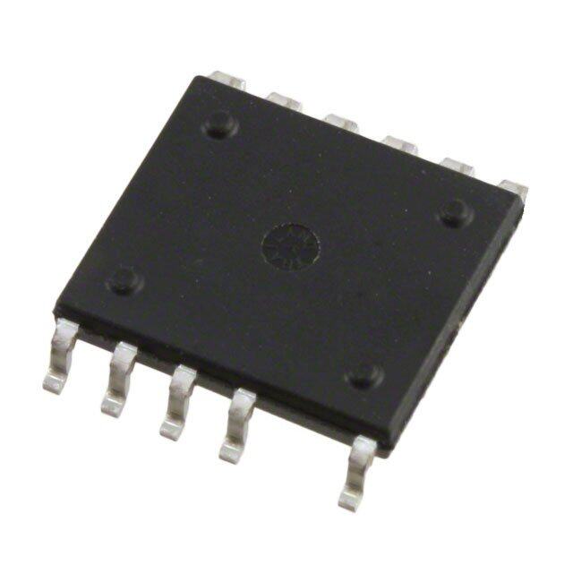
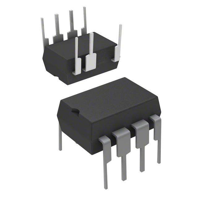
ICGOO在线商城 > 集成电路(IC) > PMIC - AC-DC 转换器,离线开关 > FAN7621SJX
- 型号: FAN7621SJX
- 制造商: Fairchild Semiconductor
- 库位|库存: xxxx|xxxx
- 要求:
| 数量阶梯 | 香港交货 | 国内含税 |
| +xxxx | $xxxx | ¥xxxx |
查看当月历史价格
查看今年历史价格
FAN7621SJX产品简介:
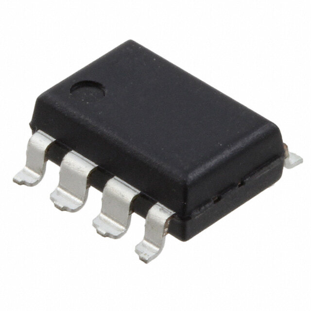
ICGOO电子元器件商城为您提供FAN7621SJX由Fairchild Semiconductor设计生产,在icgoo商城现货销售,并且可以通过原厂、代理商等渠道进行代购。 FAN7621SJX价格参考。Fairchild SemiconductorFAN7621SJX封装/规格:PMIC - AC-DC 转换器,离线开关, Converter Offline Half-Bridge Topology Up to 300kHz 16-SOP。您可以下载FAN7621SJX参考资料、Datasheet数据手册功能说明书,资料中有FAN7621SJX 详细功能的应用电路图电压和使用方法及教程。
| 参数 | 数值 |
| 产品目录 | 集成电路 (IC)半导体 |
| 描述 | IC OFF-LINE CTRLR PROG PFM 16SOP交流/直流转换器 PWM Control IC for High Power FPS |
| 产品分类 | |
| 品牌 | Fairchild Semiconductor |
| 产品手册 | |
| 产品图片 |
|
| rohs | 符合RoHS无铅 / 符合限制有害物质指令(RoHS)规范要求 |
| 产品系列 | 电源管理 IC,交流/直流转换器,Fairchild Semiconductor FAN7621SJX- |
| 数据手册 | |
| 产品型号 | FAN7621SJX |
| 上升时间 | 65 ns |
| 下降时间 | 35 ns |
| 产品 | Driver ICs - Various |
| 产品目录页面 | |
| 产品种类 | 交流/直流转换器 |
| 供应商器件封装 | 16-SOP |
| 其它名称 | FAN7621SJXCT |
| 功率(W) | - |
| 包装 | 剪切带 (CT) |
| 单位重量 | 242 mg |
| 商标 | Fairchild Semiconductor |
| 安装风格 | SMD/SMT |
| 封装 | Reel |
| 封装/外壳 | 16-SOIC(0.209",5.30mm 宽) |
| 封装/箱体 | SOP-16 |
| 工作温度 | -40°C ~ 130°C |
| 工厂包装数量 | 2000 |
| 最大功率耗散 | 1.13 W |
| 最大工作温度 | + 130 C |
| 最小工作温度 | - 40 C |
| 标准包装 | 1 |
| 激励器数量 | 2 |
| 特色产品 | http://www.digikey.cn/product-highlights/cn/zh/fairchild-semiconductor-led-solutions/3901 |
| 电压-击穿 | - |
| 电压-输入 | 8.7 V ~ 25 V |
| 电压-输出 | - |
| 电源电压-最大 | 25 V |
| 电源电压-最小 | - 0.3 V |
| 电源电流 | 6 mA |
| 类型 | PFM Controller for Half-Bridge Resonant Converters |
| 系列 | FAN7621 |
| 输出电压 | 1 V |
| 输出电流 | 600 mA |
| 输出端数量 | 2 |
| 输出隔离 | 隔离 |
| 频率范围 | 94kHz ~ 106kHz |

PDF Datasheet 数据手册内容提取
Is Now Part of To learn more about ON Semiconductor, please visit our website at www.onsemi.com Please note: As part of the Fairchild Semiconductor integration, some of the Fairchild orderable part numbers will need to change in order to meet ON Semiconductor’s system requirements. Since the ON Semiconductor product management systems do not have the ability to manage part nomenclature that utilizes an underscore (_), the underscore (_) in the Fairchild part numbers will be changed to a dash (-). This document may contain device numbers with an underscore (_). Please check the ON Semiconductor website to verify the updated device numbers. The most current and up-to-date ordering information can be found at www.onsemi.com. Please email any questions regarding the system integration to Fairchild_questions@onsemi.com. ON Semiconductor and the ON Semiconductor logo are trademarks of Semiconductor Components Industries, LLC dba ON Semiconductor or its subsidiaries in the United States and/or other countries. ON Semiconductor owns the rights to a number of patents, trademarks, copyrights, trade secrets, and other intellectual property. A listing of ON Semiconductor’s product/patent coverage may be accessed at www.onsemi.com/site/pdf/Patent-Marking.pdf. ON Semiconductor reserves the right to make changes without further notice to any products herein. ON Semiconductor makes no warranty, representation or guarantee regarding the suitability of its products for any particular purpose, nor does ON Semiconductor assume any liability arising out of the application or use of any product or circuit, and specifically disclaims any and all liability, including without limitation special, consequential or incidental damages. Buyer is responsible for its products and applications using ON Semiconductor products, including compliance with all laws, regulations and safety requirements or standards, regardless of any support or applications information provided by ON Semiconductor. “Typical” parameters which may be provided in ON Semiconductor data sheets and/or specifications can and do vary in different applications and actual performance may vary over time. All operating parameters, including “Typicals” must be validated for each customer application by customer’s technical experts. ON Semiconductor does not convey any license under its patent rights nor the rights of others. ON Semiconductor products are not designed, intended, or authorized for use as a critical component in life support systems or any FDA Class 3 medical devices or medical devices with a same or similar classification in a foreign jurisdiction or any devices intended for implantation in the human body. Should Buyer purchase or use ON Semiconductor products for any such unintended or unauthorized application, Buyer shall indemnify and hold ON Semiconductor and its officers, employees, subsidiaries, affiliates, and distributors harmless against all claims, costs, damages, and expenses, and reasonable attorney fees arising out of, directly or indirectly, any claim of personal injury or death associated with such unintended or unauthorized use, even if such claim alleges that ON Semiconductor was negligent regarding the design or manufacture of the part. ON Semiconductor is an Equal Opportunity/Affirmative Action Employer. This literature is subject to all applicable copyright laws and is not for resale in any manner.
F A N 7 6 July 2010 2 1 — P FAN7621 F M C PFM Controller for Half-Bridge Resonant Converters o n t r o Features Description l l e r (cid:131) Variable Frequency Control with 50% Duty Cycle The FAN7621 is a pulse frequency modulation controller f for high-efficiency half-bridge resonant converters. o for Half-bridge Resonant Converter Topology r Offering everything necessary to build a reliable and (cid:131) High Efficiency through Zero Voltage Switching (ZVS) H robust resonant converter, the FAN7621 simplifies a (cid:131) Fixed Dead Time (350ns) designs and improves productivity, while improving lf - (cid:131) Up to 300kHz Operating Frequency performance. The FAN7621 includes a high-side gate- B (cid:131) Pulse Skipping for Frequency Limit (Programmable) drive circuit, an accurate current controlled oscillator, rid at Light-Load Condition frequency limit circuit, soft-start, and built-in protection g functions. The high-side gate-drive circuit has a e (cid:131) Remote On/Off Control Using CON Pin common-mode noise cancellation capability, which R (cid:131) Protection Functions: Over-Voltage Protection guarantees stable operation with excellent noise e s (OVP), Overload Protection (OLP), Over-Current immunity. Using the zero-voltage-switching (ZVS) o technique dramatically reduces the switching losses and n Protection (OCP), Abnormal Over-Current Protection a efficiency is significantly improved. The ZVS also n (AOCP), Internal Thermal Shutdown (TSD) reduces the switching noise noticeably, which allows a t C small-sized Electromagnetic Interference (EMI) filter. Applications o n The FAN7621 can be applied to various resonant v (cid:131) PDP and LCD TVs converter topologies; such as series resonant, parallel e r (cid:131) Desktop PCs and Servers resonant, and LLC resonant converters. te r (cid:131) Adapters s (cid:131) Telecom Power Supplies Related Resources (cid:131) Video Game Consoles AN4151 — Half-bridge LLC Resonant Converter Design using FSFR-series Fairchild Power Switch (FPSTM) Ordering Information Operating Junction Part Number Package Packaging Method Temperature FAN7621N 16-Lead, Dual Inline Package (DIP) Tube FAN7621SJ -40°C ~ 130°C 16-Lead, Small-Outline Package (SOP) Tube FAN7621SJX 16-Lead, Small-Outline Package (SOP) Tape & Reel © 2009 Fairchild Semiconductor Corporation www.fairchildsemi.com FAN7621 • Rev. 1.0.3
F A Application Circuit Diagram N 7 6 D1 2 1 Cr — L P lk Np Ns VO F M V CC LVcc Lm C o HVCC Ns n t RT r 1 o 2 l 6 HO le CON N7 D2 CF RF r CDL A CTR fo V F r IN KA431 H LO a CS lf - B SG PG r i d g e R R sense e s o Figure 1. Typical Application Circuit (LLC Resonant Half-Bridge Converter) n a n t C o Block Diagram n v e LVCC r t 12 e r s + LV good VREF ICTC + 11.3/14.5V - CC VREF 8.7/9.2V 3V - S Q Internal HVCCgood - ICTC 2ICTC 1V + RF/F-Q Bias + 1 HVCC - + 2V Time Level-Shift High-Side 3 HO Delay GateDrive - 350ns RT 8 2 CTR LV Counter(1/4) CC I OLP CON 6 - DTeimlaey BaDlaenlacying GLaotwe-DSirdivee 14 LO 0.4/0.6V + 350ns + OLP Shutdownwithoutdelay 5V - S Q LVCC + LVCCgood AutRo-re-Qstart Q S 50nsDelay + -1 O23VVP - Protection -Q R - VAOC0.P9V Latch TSD 16 PG Protection LV <5V CC V OCP Delay - 0.58V 10 SG 1.5µs + 9 CS Figure 2. Internal Block Diagram © 2009 Fairchild Semiconductor Corporation www.fairchildsemi.com FAN7621 • Rev. 1.0.3 2
F A Pin Configuration N 7 6 2 1 — P (1) HV PG (16) CC F M C (2) CTR NC (15) o n t r (3) HO LO (14) o l l e r f (4) NC NC (13) o r FAN7621 H a (5) NC LV (12) l CC f - B r (6) CON NC (11) id g e R (7) NC SG (10) e s o n (8) RT CS (9) a n t C o Figure 3. Package Diagram n v e r t Pin Definitions e r s Pin # Name Description 1 HV This is the supply voltage of the high-side gate-drive circuit IC. CC 2 CTR This is the drain of the low-side MOSFET. Typically, a transformer is connected to this pin. 3 HO This is the high-side gate driving signal. 4 NC No connection. 5 NC No connection. This pin is for a protection and enabling/disabling the controller. When the voltage of this pin is above 0.6V, the IC operation is enabled. When the voltage of this pin drops below 0.4V, 6 CON gate drive signals for both MOSFETs are disabled. When the voltage of this pin increases above 5V, protection is triggered. 7 NC No connection. This pin programs the switching frequency. Typically, an opto-coupler is connected to 8 R T control the switching frequency for the output voltage regulation. This pin senses the current flowing through the low-side MOSFET. Typically, negative 9 CS voltage is applied on this pin. 10 SG This pin is the control ground. 11 NC No connection. 12 LV This pin is the supply voltage of the control IC. CC 13 NC No connection. 14 LO This is the low-side gate driving signal. 15 NC No connection. 16 PG This pin is the power ground. This pin is connected to the source of the low-side MOSFET. © 2009 Fairchild Semiconductor Corporation www.fairchildsemi.com FAN7621 • Rev. 1.0.3 3
F A Absolute Maximum Ratings N 7 Stresses exceeding the absolute maximum ratings may damage the device. The device may not function or be 6 2 operable above the recommended operating conditions and stressing the parts to these levels is not recommended. In 1 addition, extended exposure to stresses above the recommended operating conditions may affect device reliability. — The absolute maximum ratings are stress ratings only. TA=25°C unless otherwise specified. P F Symbol Parameter Min. Max. Unit M V High-Side Gate Driving Voltage V -0.3 HV C HO CTR CC V o V Low-Side Gate Driving Voltage -0.3 LV n LO CC t r LVCC Low-Side Supply Voltage -0.3 25.0 V o l l HV to V High-Side V Pin to Center Voltage -0.3 25.0 V e CC CTR CC r V Center Voltage -0.3 600.0 V f CTR o r VCON Control Pin Input Voltage -0.3 LVCC V H V Current Sense (CS) Pin Input Voltage -5.0 1.0 V a CS l f VRT RT Pin Input Voltage -0.3 5.0 V -B r dV /dt Allowable Center Voltage Slew Rate 50 V/ns i CTR d g 16-DIP 1.56 W e PD Total Power Dissipation 16-SOP 1.13 W R e Maximum Junction Temperature(1) +150 s TJ Recommended Operating Junction Temperature(1) -40 +130 °C on a n TSTG Storage Temperature Range -55 +150 °C t C Note: o 1. The maximum value of the recommended operating junction temperature is limited by thermal shutdown. n v e r t e r Thermal Impedance s Symbol Parameter Value Unit 16-DIP 80 θ Junction-to-Ambient Thermal Impedance ºC/W JA 16-SOP 110 © 2009 Fairchild Semiconductor Corporation www.fairchildsemi.com FAN7621 • Rev. 1.0.3 4
F A Electrical Characteristics N 7 T =25°C and LV =17V unless otherwise specified. 6 A CC 2 1 Symbol Parameter Test Conditions Min. Typ. Max. Unit — Supply Section P F I Offset Supply Leakage Current HV =V 50 μA M LK CC CTR C I HV Quiescent HV Supply Current (HV UV+) - 0.1V 50 120 μA Q CC CC CC o n IQLVCC Quiescent LVCC Supply Current (LVCCUV+) - 0.1V 100 200 μA t r o IOHVCC O(RpMeSra tVinaglu He)V CC Supply Current fCOLSoCa=d=110n0FkH z, VCON > 0.6V, 5 8 mA ller No Switching, VCON < 0.4V 100 200 μA fo r fOSC=100kHz, VCON > 0.6V, 6 9 mA H I LV Operating LVCC Supply Current CLoad=1nF a O CC (RMS Value) lf No Switching, VCON < 0.4V 2 4 mA -B r UVLO Section id g LV UV+ LV Supply Under-Voltage Positive Going Threshold (LV Start) 13.0 14.5 16.0 V e CC CC CC R LVCCUV- LVCC Supply Under-Voltage Negative Going Threshold (LVCC Stop) 10.2 11.3 12.4 V e s LV UVH LV Supply Under-Voltage Hysteresis 3.2 V o CC CC n a HV UV+ HV Supply Under-Voltage Positive Going Threshold (HV Start) 8.2 9.2 10.2 V CC CC CC n t HVCCUV- HVCC Supply Under-Voltage Negative Going Threshold (HVCC Stop) 7.8 8.7 9.6 V C o HVCCUVH HVCC Supply Under-Voltage Hysteresis 0.5 V n v Oscillator & Feedback Section e r t e VCONDIS Control Pin Disable Threshold Voltage 0.36 0.40 0.44 V r s V Control Pin Enable Threshold Voltage 0.54 0.60 0.66 V CONEN V V-I Converter Threshold Voltage 1.5 2.0 2.5 V RT fOSC Output Oscillation Frequency RT=5.2kΩ 94 100 106 kHz DC Output Duty Cycle 48 50 52 % fSS Internal Soft-Start Initial Frequency fSS=fOSC+40kHz, RT=5.2kΩ 140 kHz t Internal Soft-Start Time 2 3 4 ms SS Output Section I Peak Sourcing Current HV =17V 250 360 mA source CC I Peak Sinking Current HV =17V 460 600 mA sink CC t Rising Time 65 ns r C =1nF, HV =17V Load CC t Falling Time 35 ns f High Level of High-Side Gate Driving V 1.0 V HOH Signal (V -V ) HVCC HO Low Level of High-Side Gate Driving V 0.6 V HOL Signal I =20mA O High Level of High-Side Gate Driving V 1.0 V LOH Signal (V -V ) LVCC LO Low Level of High-Side Gate Driving V 0.6 V LOL Signal © 2009 Fairchild Semiconductor Corporation www.fairchildsemi.com FAN7621 • Rev. 1.0.3 5
F A Electrical Characteristics (Continued) N 7 T =25°C and LV =17V unless otherwise specified. 6 A CC 2 1 Symbol Parameter Test Conditions Min. Typ. Max. Unit — Protection Section P F I OLP Delay Current V =4V 3.8 5.0 6.2 μA M OLP CON C VOLP OLP Protection Voltage VCON > 3.5V 4.5 5.0 5.5 V o n VOVP LVCC Over-Voltage Protection LVCC > 21V 21 23 25 V tr o V AOCP Threshold Voltage -1.0 -0.9 -0.8 V l AOCP l e r tBAO AOCP Blanking Time 50 ns f o V OCP Threshold Voltage -0.64 -0.58 -0.52 V r OCP H t OCP Blanking Time(2) 1.0 1.5 2.0 μs a BO l f - Delay Time (Low-Side) Detecting from B tDA V to Switch Off(2) 250 400 ns r AOCP i d TSD Thermal Shutdown Temperature(2) 110 130 150 °C ge Protection Latch Sustain LV Supply R ISU Current CC LVCC=7.5V 100 150 μA e s o VPRSET PVorolttaegceti on Latch Reset LVCC Supply 5 V na n t Dead-Time Control Section C o DT Dead Time 350 ns n v Note: e r 2. These parameters, although guaranteed, are not tested in production. t e r s © 2009 Fairchild Semiconductor Corporation www.fairchildsemi.com FAN7621 • Rev. 1.0.3 6
F A Typical Performance Characteristics N 7 6 These characteristic graphs are normalized at T =25ºC. 2 A 1 — 1.1 1.1 P F M 1.05 1.05 C C o O5 C n at 2 O25 tr alized 1 zed at 1 olle orm mali r f N0.95 or 0.95 o N r H a l 0.9 0.9 f- -50 -25 0 25 50 75 100 -50 -25 0 25 50 75 100 B r Temp (OC) Temp (OC) id g Figure 4. Low-Side MOSFET Duty Cycle Figure 5. Switching Frequency vs. Temperature e vs. Temperature R e s o 1.1 1.1 n a n t C 1.05 1.05 o n C C v Omalized at 25 1 Omalized at 25 1 erters or 0.95 or0.95 N N 0.9 0.9 -50 -25 0 25 50 75 100 -50 -25 0 25 50 75 100 Temp (OC) Temp (OC) Figure 6. High-Side V (HV ) Start vs. Temperature Figure 7. High-Side V (HV ) Stop vs. Temperature CC CC CC CC 1.1 1.1 1.05 1.05 C C Od at 25 1 Od at 25 1 malize malize or0.95 or0.95 N N 0.9 0.9 -50 -25 0 25 50 75 100 -50 -25 0 25 50 75 100 Temp (OC) Temp (OC) Figure 8. Low-Side V (LV ) Start vs. Temperature Figure 9. Low-Side V (LV ) Stop vs. Temperature CC CC CC CC © 2009 Fairchild Semiconductor Corporation www.fairchildsemi.com FAN7621 • Rev. 1.0.3 7
F A Typical Performance Characteristics N (Continued) 7 6 These characteristic graphs are normalized at T =25ºC. 2 A 1 — 1.1 1.1 P F M 1.05 1.05 C o C C n Omalized at 25 1 Omalized at 25 1 troller f or0.95 or0.95 o N N r H a l 0.9 0.9 f- B -50 -25 0 25 50 75 100 -50 -25 0 25 50 75 100 r Temp (OC) Temp (OC) id g e Figure 10. OLP Delay Current vs. Temperature Figure 11. OLP Protection Voltage vs. Temperature R e s 1.1 1.1 o n a n 1.05 1.05 t C Omalized at 25C 1 Omalized at 25C 1 onverters Nor0.95 Nor0.95 0.9 0.9 -50 -25 0 25 50 75 100 -50 -25 0 25 50 75 100 Temp (OC) Temp (OC) Figure 12. LV OVP Voltage vs. Temperature Figure 13. R Voltage vs. Temperature CC T 1.1 1.1 1.05 1.05 C C Omalized at 25 1 Omalized at 25 1 Nor0.95 Nor0.95 0.9 0.9 -50 -25 0 25 50 75 100 -50 -25 0 25 50 75 100 Temp (OC) Temp (OC) Figure 14. CON Pin Enable Voltage vs. Temperature Figure 15. OCP Voltage vs. Temperature © 2009 Fairchild Semiconductor Corporation www.fairchildsemi.com FAN7621 • Rev. 1.0.3 8
F Functional Description A N Gain 7 1. Basic Operation 6 2 1 FAN7621 is designed to drive high-side and low-side 1.8 — MOSFETs complementarily with 50% duty cycle. A fixed dead time of 350ns is introduced between consecutive f min f normal f max f ISS P transitions, as shown in Figure 16. F 1.6 M Dead time C High-side 1.4 o n MOSFET t r gatedrive o 1.2 ll e r f o Low-side 1.0 r MOSFET Soft-start H gatedrve a time 0.8 lf- Figure 16. MOSFETs Gate Drive Signal B r i d 0.6 g 60 70 80 90 100 110 120 130 140 150 e Frequency (kHz) R 2. Internal Oscillator e Figure 18. Resonant Converter Typical Gain Curve s FAN7621 employs a current-controlled oscillator, as o shown in Figure 17. Internally, the voltage of R pin is n T a regulated at 2V and the charging / discharging current n for the oscillator capacitor, CT, is obtained by copying the VCC t C current flowing out of RT pin (ICTC) using a current mirror. LVCC o Therefore, the switching frequency increases as ICTC HV n increases. CC v e RT r 1 t e V I Rmax Rmin RSS 62 HO rs REF CTC + 7 S Q CON N 3V - C A CTR I R -Q SS CTC 2ICTC 1V + F C F/F T LO - CS + 2V SG PG RT - C(o1u/4n)t er 8 Gatedrive R sense Figure 17. Current Controlled Oscillator Figure 19. Frequency Control Circuit The minimum switching frequency is determined as: 5.2kΩ 3. Frequency Setting fmin = ×100(kHz) (1) R min Figure 18 shows the typical voltage gain curve of a Assuming the saturation voltage of opto-coupler resonant converter, where the gain is inversely transistor is 0.2V, the maximum switching frequency is proportional to the switching frequency in the ZVS determined as: region. The output voltage can be regulated by modulating the switching frequency. Figure 19 shows the 5.2kΩ 4.68kΩ typical circuit configuration for R pin, where the opto- fmax =( + )×100(kHz) (2) T R R coupler transistor is connected to the RT pin to modulate min max the switching frequency. To prevent excessive inrush current and overshoot of output voltage during startup, increase the voltage gain of the resonant converter progressively. Since the voltage gain of the resonant converter is inversely proportional to the switching frequency, the soft-start is © 2009 Fairchild Semiconductor Corporation www.fairchildsemi.com FAN7621 • Rev. 1.0.3 9
F implemented by sweeping down the switching frequency A from an initial high frequency (fISS) until the output N voltage is established. The soft-start circuit is made by V 7 CC 6 cino nFnigeucrtein g1 9R. -FCA Nse7r6ie2s1 naelstwo ohrak so ann t hinet eRrnT apl ins,o fat-ss tsahrot wfonr LVCC 21 3ms to reduce the current overshoot during the initial HVCC — cycles, which adds 40kHz to the initial frequency of the RT P external soft-start circuit, as shown in Figure 20. The 1 F initial frequency of the soft-start is given as: Rmax Rmin RSS 762 HO M C fISS =(5.2kΩ+5.2kΩ)×100+40(kHz) (3) CON N o Rmin RSS CSS FA CTR ntr o It is typical to set the initial (soft-start) frequency of two ~ l three times the resonant frequency (f ) of the resonant LO le network. O CS r f o The soft-start time is three to four times the RC time r SG PG H constant. The RC time constant is as follows: a l T =R ⋅C (4) f- SS SS SS B f Figure 22. Control Pin Configuration for r s i Pulse Skipping d g fISS e 40kHz Remote On / Off: When an auxiliary power supply is R used for standby, the main power stage using FAN7621 Control loop e take over can be shut down by pulling down the control pin s voltage, as shown in Figure 23. R1 and C1 are used to o n ensure soft-start when switching resumes. a n t Main C time OP1 Output on Figure 20. Frequency Sweeping of Soft-Start R1 v e r t 4. Control Pin e C1 r s The FAN7621 has a control pin for protection, cycle skipping, and remote on/off. Figure 21 shows the internal FAN7621 Main Off block diagram for control pin. LV CC R IOLP T Rmin OAuutpxut CON 6 - 0.4/0.6V + + StopSwitching CON OLP 5V - S Q R -Q LVCC + OP1 23V - LVCCgood Apurtoot-ercetsiotanrt OVP Figure 23. Remote On / Off Circuit Figure 21. Internal Block of Control Pin 5. Protection Circuits Protection: When the control pin voltage exceeds 5V, protection is triggered. Detailed applications are The FAN7621 has several self-protective functions, such described in the protection section. as Overload Protection (OLP), Over-Current Protection (OCP), Abnormal Over-Current Protection (AOCP), Pulse Skipping: FAN7621 stops switching when the Over-Voltage Protection (OVP), and Thermal Shutdown control pin voltage drops below 0.4V and resumes (TSD). OLP, OCP, and OVP are auto-restart mode switching when the control pin voltage rises above 0.6V. protections; while AOCP and TSD are latch-mode To use pulse-skipping, the control pin should be protections, as shown in Figure 24. connected to the opto-coupler collector pin. The frequency that causes pulse skipping is given as: 5.1 Auto-Restart Mode Protection: Once a fault condition is detected, switching is terminated and the SKIP = 5.2k + 4.16k x100(kHz) (5) MOSFETs remain off. When LVCC falls to the LVCC stop R R voltage of 11.3V, the protection is reset. FAN7621 min max © 2009 Fairchild Semiconductor Corporation www.fairchildsemi.com FAN7621 • Rev. 1.0.3 10
F resumes normal operation when LVCC reaches the start 5.4 Current Sensing Using Resonant Capacitor A voltage of 14.5V. Voltage: For high-power applications, current sensing N using a resistor may not be available due to the severe 7 5.2 Latch-Mode Protection: Once this protection is 6 power dissipation in the resistor. In that case, indirect 2 triggered, switching is terminated and the gate output 1 current sensing using the resonant capacitor voltage can signals remain off. The latch is reset only when LVCC is be a good alternative because the amplitude of the — discharged below 5V. resonant capacitor voltage (Vcrp-p) is proportional to the P LVCC resonant current in the primary side (Ipp-p) as: FM 12 I p−p 11/14V +- LVCC good VRE F InB teiarnsal VCrp−p = 2πpfsCr (6) Con t r To minimize power dissipation, a capacitive voltage o Shutdown divider is generally used for capacitor voltage sensing, lle OCP Auto-restart La tch as shown in Figure 27. r f OLP protection protection o AOCP r OVP S Q Q S C LVCC H COLVNC Cgood RF/F-Q -QF/FR TSD DL RT HVCC alf- 20k 1 B LVCC<5V CONN762 HO Ip rid Figure 24. Protection Blocks A CTR g F e 5.3 Current Sensing Using Resistor: FAN7621 LO R senses drain current as a negative voltage, as shown in CSSG PG es Figure 25 and Figure 26. Half-wave sensing allows low o power dissipation in the sensing resistor, while full-wave Csense CB na sensing has less switching noise in the sensing signal. V 100 n sense Cr t C o I n LVCC p v HVCC er RT 1 te CDL CONN762 HO V rs A CTR Cr F V LO Ids VCrp-p CS CS SG PG VCS Vsense VVsCernps−eppk=CsenCse+BCB Vse2nsepk=VCON R sense I ds V pk sense VCON Figure 25. Half-Wave Sensing V pk sense Ids tDelay=RdCd Figure 27. Current Sensing Using Resonant Capacitor Voltage LVCC VCS 5.5 Over-Current Protection (OCP): When the HVCC sensing pin voltage drops below -0.6V, OCP is triggered RT 621 HO and the MOSFETs remain off. This protection has a CDL CONN7 shutdown time delay of 1.5µs to prevent premature ACTR shutdown during startup. F VCS LO 5.6 Abnormal Over-Current Protection (AOCP): If CS the secondary rectifier diodes are shorted, large current SG PG with extremely high di/dt can flow through the MOSFET before OCP or OLP is triggered. AOCP is triggered R without shutdown delay when the sensing pin voltage Ids sense drops below -0.9V. This protection is latch mode and reset when LV is pulled down below 5V. Figure 26. Full-Wave Sensing CC © 2009 Fairchild Semiconductor Corporation www.fairchildsemi.com FAN7621 • Rev. 1.0.3 11
F 5.7 Overload Protection (OLP): Overload is A 6. PCB Layout Guideline defined as the load current exceeding its normal level N due to an unexpected abnormal event. In this situation, Duty imbalance problems may occur due to the radiated 7 6 the protection circuit should trigger to protect the power noise from main transformer, the inequality of the 2 supply. However, even when the power supply is in the secondary-side leakage inductances of main 1 normal condition, the overload situation can occur during transformer, and so on. Among them, it is one of the — the load transition. To avoid premature triggering of dominant reasons that the control components in the P protection, the overload protection circuit should be vicinity of R pin are enclosed by the primary current flow F T designed to trigger only after a specified time to pattern on PCB layout. The direction of the magnetic M determine whether it is a transient situation or a true field on the components caused by the primary current C overload situation. Figure 27 shows a typical overload flow is changed when the high-and-low side MOSFET o n protection circuit. By sensing the resonant capacitor turns on by turns. The magnetic fields with opposite t voltage on the control pin, the overload protection can be direction from each other induce a current through, into, ro implemented. Using RC time constant, shutdown delay or out of the RT pin, which makes the turn-on duration of lle can be also introduced. The voltage obtained on the each MOSFET different. It is strongly recommended to r control pin is given as: separate the control components in the vicinity of RT pin fo from the primary current flow pattern on PCB layout. r V = CB V p−p (7) Figure 28 shows an example for the duty-balanced case. H CON 2(C +C ) Cr The yellow and blue lines show the primary current flows a B sense lf when the lower-side and higher-side MOSFETs turns on, - where V p-p is the amplitude of the resonant capacitor B Cr respectively. The primary current does not enclose any r voltage. component of controller. id g 5.8 Over-Voltage Protection (OVP): When the It is helpful to reduce the duty imbalance to make the e LVCC reaches 23V, OVP is triggered. This protection is loop configured between CON pin and opto-coupler as R used when auxiliary winding of the transformer to supply small as possible, as shown in the red line in Figure 28. e s V to the controller is utilized. CC o n 5.9 Thermal Shutdown (TSD): If the temperature a n of the junction exceeds approximately 130°C, the t thermal shutdown triggers. C o n v e r t e r s Figure 28. Example for Duty Balancing © 2009 Fairchild Semiconductor Corporation www.fairchildsemi.com FAN7621 • Rev. 1.0.3 12
F A Typical Application Circuit (Half-Bridge LLC Resonant Converter) N 7 6 2 Output Voltage 1 Application Device Input Voltage Range Rated Output Power (Rated Current) — 390V P LCD TV FAN7621 (340~400DVC ) 200W 24V-8.3A F DC M C o n Features t r o (cid:131) High efficiency ( >94% at 400VDC input) lle (cid:131) Reduced EMI noise through zero-voltage-switching (ZVS) r f (cid:131) Enhanced system reliability with various protection functions o r H a l f - B r i d g e R e s o n 21 a 6 n 7 N t A C F o n v e r t e r s Figure 29. Typical Application Circuit © 2009 Fairchild Semiconductor Corporation www.fairchildsemi.com FAN7621 • Rev. 1.0.3 13
F A Typical Application Circuit (Continued) N 7 6 Usually, LLC resonant converters require large leakage inductance value. To obtain a large leakage inductance, 2 1 sectional winding method is used. — (cid:131) Core: EC35 (Ae=106 mm2) P (cid:131) Bobbin: EC35 (Horizontal) F M (cid:131) Transformer Model Number: SNX-2468-1 C o n EC35 t r o l l e 2 Np 13 Ns2 r fo 12 r Ns1 H a l f 10 - B r 6 9 id g e R e s Figure 30. Transformer Construction o n a n t Pins (S → F) Wire Turns Note C o n N 6 → 2 0.08φ×88 (Litz Wire) 36 p v e Ns1 12 → 9 0.08φ×234 (Litz Wire) 4 Bifilar Winding rte r N 10 → 13 0.08φ×234 (Litz Wire) 4 Bifilar Winding s s2 Pins Specifications Remark Primary-Side Inductance (Lp) 2-6 550μH ± 10% 100kHz, 1V Primary-Side Effective Leakage (Lr) 2-6 110μH ± 10% Short one of the secondary windings For more detailed information regarding the transformer, visit http://www.santronics-usa.com/documents.html or contact sales@santronics-usa.com or +1-408-734-1878 (Sunnyvale, California USA). © 2009 Fairchild Semiconductor Corporation www.fairchildsemi.com FAN7621 • Rev. 1.0.3 14
10.30 10.10 0.47 TYP -A- 16 9 16 15 10 9 5.40 5.01 TYP 7.8 -B- 5.20 9.27 TYP 1 2 7 8 3.9 (2.13 TYP) 0.2 C B A 1 8 ALL LEAD TIPS PIN 1 IDENT. 1.27 0.60 TYP TYP ALL LEAD TIPS 0.1 C SEE DETAIL A 0.16 1.90 0.25 2.1 MAX 0.14 1.70 0.15 0.51 0.35 1.27 TYP 0.12 C A NOTES: A. CONFORMS TO EIAJ EDR-7320 REGISTRATION, ESTABLISHED IN DECEMBER, 1998. B. DIMENSIONS ARE IN MILLIMETERS. 7° TYP C. DIMENSIONS ARE EXCLUSIVE OF BURRS, MOLD FLASH, AND TIE BAR EXTRUSIONS. GAGE PLANE D. DRAWING FILENAME: MKT-M16Drev5 0-8° TYP 0.25 MIN SEATING PLANE 0.25 1.25
ON Semiconductor and are trademarks of Semiconductor Components Industries, LLC dba ON Semiconductor or its subsidiaries in the United States and/or other countries. ON Semiconductor owns the rights to a number of patents, trademarks, copyrights, trade secrets, and other intellectual property. A listing of ON Semiconductor’s product/patent coverage may be accessed at www.onsemi.com/site/pdf/Patent−Marking.pdf. ON Semiconductor reserves the right to make changes without further notice to any products herein. ON Semiconductor makes no warranty, representation or guarantee regarding the suitability of its products for any particular purpose, nor does ON Semiconductor assume any liability arising out of the application or use of any product or circuit, and specifically disclaims any and all liability, including without limitation special, consequential or incidental damages. Buyer is responsible for its products and applications using ON Semiconductor products, including compliance with all laws, regulations and safety requirements or standards, regardless of any support or applications information provided by ON Semiconductor. “Typical” parameters which may be provided in ON Semiconductor data sheets and/or specifications can and do vary in different applications and actual performance may vary over time. All operating parameters, including “Typicals” must be validated for each customer application by customer’s technical experts. ON Semiconductor does not convey any license under its patent rights nor the rights of others. ON Semiconductor products are not designed, intended, or authorized for use as a critical component in life support systems or any FDA Class 3 medical devices or medical devices with a same or similar classification in a foreign jurisdiction or any devices intended for implantation in the human body. Should Buyer purchase or use ON Semiconductor products for any such unintended or unauthorized application, Buyer shall indemnify and hold ON Semiconductor and its officers, employees, subsidiaries, affiliates, and distributors harmless against all claims, costs, damages, and expenses, and reasonable attorney fees arising out of, directly or indirectly, any claim of personal injury or death associated with such unintended or unauthorized use, even if such claim alleges that ON Semiconductor was negligent regarding the design or manufacture of the part. ON Semiconductor is an Equal Opportunity/Affirmative Action Employer. This literature is subject to all applicable copyright laws and is not for resale in any manner. PUBLICATION ORDERING INFORMATION LITERATURE FULFILLMENT: N. American Technical Support: 800−282−9855 Toll Free ON Semiconductor Website: www.onsemi.com Literature Distribution Center for ON Semiconductor USA/Canada 19521 E. 32nd Pkwy, Aurora, Colorado 80011 USA Europe, Middle East and Africa Technical Support: Order Literature: http://www.onsemi.com/orderlit Phone: 303−675−2175 or 800−344−3860 Toll Free USA/Canada Phone: 421 33 790 2910 Fax: 303−675−2176 or 800−344−3867 Toll Free USA/Canada Japan Customer Focus Center For additional information, please contact your local Email: orderlit@onsemi.com Phone: 81−3−5817−1050 Sales Representative © Semiconductor Components Industries, LLC www.onsemi.com www.onsemi.com 1
Mouser Electronics Authorized Distributor Click to View Pricing, Inventory, Delivery & Lifecycle Information: O N Semiconductor: FAN7621N FAN7621SJX FAN7621SJ
 Datasheet下载

