ICGOO在线商城 > 集成电路(IC) > PMIC - LED 驱动器 > FAN5624UMPX
- 型号: FAN5624UMPX
- 制造商: Fairchild Semiconductor
- 库位|库存: xxxx|xxxx
- 要求:
| 数量阶梯 | 香港交货 | 国内含税 |
| +xxxx | $xxxx | ¥xxxx |
查看当月历史价格
查看今年历史价格
FAN5624UMPX产品简介:
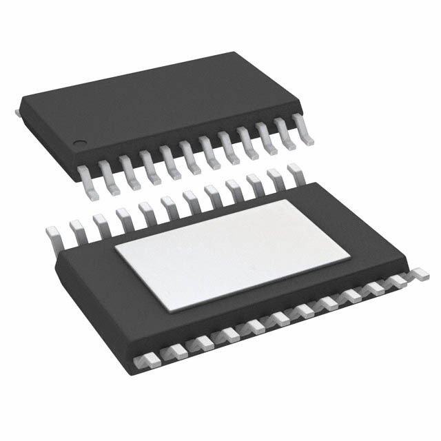
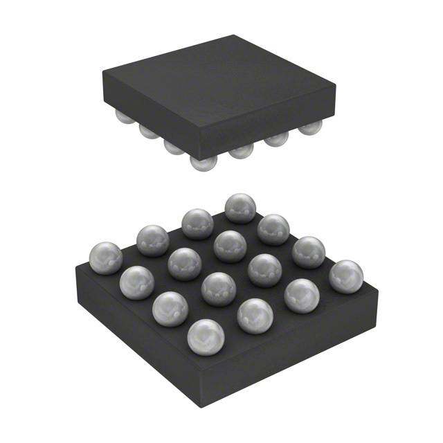
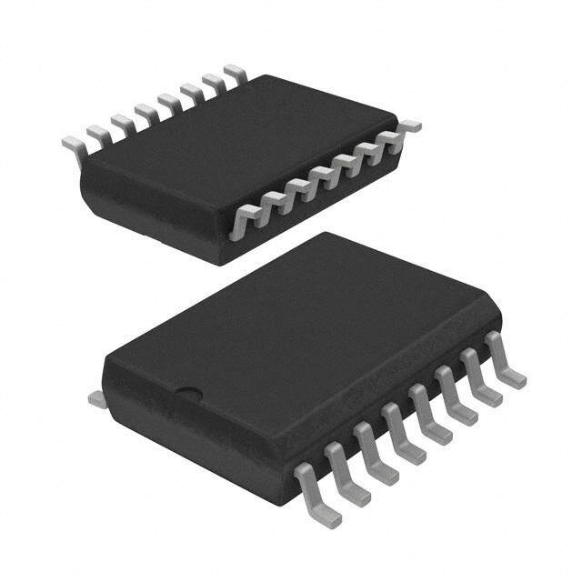
ICGOO电子元器件商城为您提供FAN5624UMPX由Fairchild Semiconductor设计生产,在icgoo商城现货销售,并且可以通过原厂、代理商等渠道进行代购。 FAN5624UMPX价格参考。Fairchild SemiconductorFAN5624UMPX封装/规格:PMIC - LED 驱动器, LED 驱动器 IC 4 输出 线性 单线 调光 30mA 10-UMLP(1.8x1.4)。您可以下载FAN5624UMPX参考资料、Datasheet数据手册功能说明书,资料中有FAN5624UMPX 详细功能的应用电路图电压和使用方法及教程。
| 参数 | 数值 |
| 产品目录 | 集成电路 (IC)光电子产品 |
| 描述 | IC LED DVR 4CH INTERFACE 10-UMLPLED照明驱动器 4Ch Linear LED Drvr w/Sngl Wire Digital |
| 产品分类 | |
| 品牌 | Fairchild Semiconductor |
| 产品手册 | |
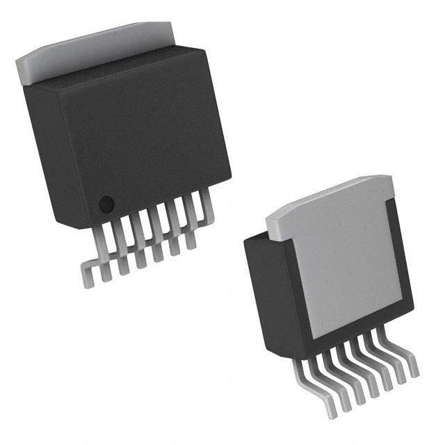
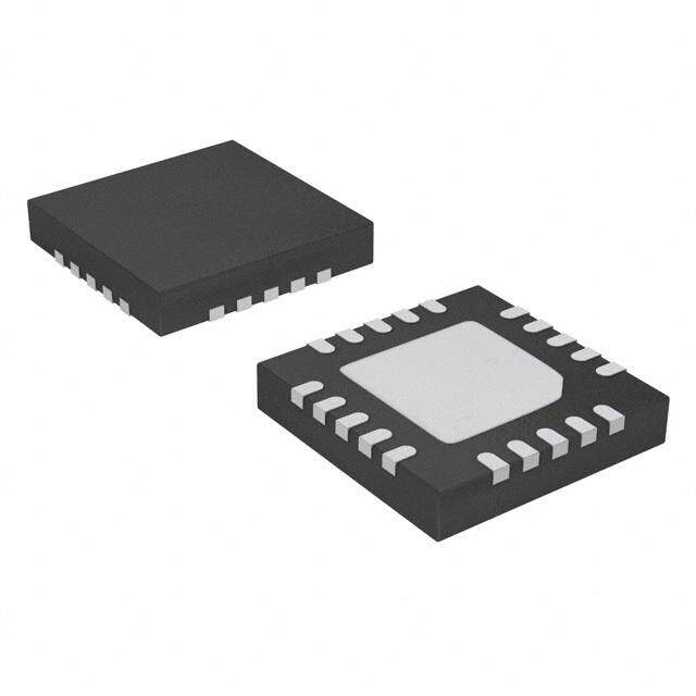
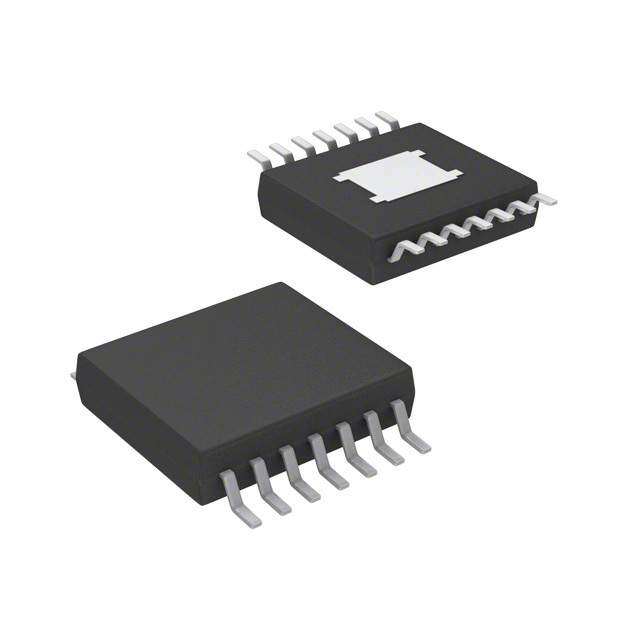
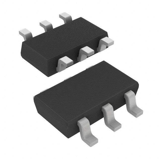
| 产品图片 |
|
| rohs | 符合RoHS无铅 / 符合限制有害物质指令(RoHS)规范要求 |
| 产品系列 | LED照明电子器件,LED照明驱动器,Fairchild Semiconductor FAN5624UMPX- |
| 数据手册 | |
| 产品型号 | FAN5624UMPX |
| PCN设计/规格 | |
| 产品种类 | LED照明驱动器 |
| 供应商器件封装 | 10-UMLP (1.8x1.4) |
| 其它名称 | FAN5624UMPXDKR |
| 内部驱动器 | 是 |
| 功率耗散 | 132 mW |
| 包装 | Digi-Reel® |
| 单位重量 | 40 mg |
| 商标 | Fairchild Semiconductor |
| 安装类型 | 表面贴装 |
| 安装风格 | SMD/SMT |
| 封装 | Reel |
| 封装/外壳 | 10-UFQFN |
| 封装/箱体 | uMLP-10 |
| 工作温度 | -40°C ~ 85°C |
| 工厂包装数量 | 5000 |
| 恒压 | - |
| 恒流 | 是 |
| 拓扑 | 线性(LDO) |
| 最大工作温度 | + 85 C |
| 最大电源电流 | 1 mA |
| 最小工作温度 | - 40 C |
| 标准包装 | 1 |
| 电压-电源 | 2.7 V ~ 5.5 V |
| 电压-输出 | - |
| 类型-初级 | 背光 |
| 类型-次级 | - |
| 系列 | FAN5624 |
| 输入电压 | 2.7 V to 5.5 V |
| 输出数 | 4 |
| 频率 | - |





- 商务部:美国ITC正式对集成电路等产品启动337调查
- 曝三星4nm工艺存在良率问题 高通将骁龙8 Gen1或转产台积电
- 太阳诱电将投资9.5亿元在常州建新厂生产MLCC 预计2023年完工
- 英特尔发布欧洲新工厂建设计划 深化IDM 2.0 战略
- 台积电先进制程称霸业界 有大客户加持明年业绩稳了
- 达到5530亿美元!SIA预计今年全球半导体销售额将创下新高
- 英特尔拟将自动驾驶子公司Mobileye上市 估值或超500亿美元
- 三星加码芯片和SET,合并消费电子和移动部门,撤换高东真等 CEO
- 三星电子宣布重大人事变动 还合并消费电子和移动部门
- 海关总署:前11个月进口集成电路产品价值2.52万亿元 增长14.8%



PDF Datasheet 数据手册内容提取
Is Now Part of To learn more about ON Semiconductor, please visit our website at www.onsemi.com Please note: As part of the Fairchild Semiconductor integration, some of the Fairchild orderable part numbers will need to change in order to meet ON Semiconductor’s system requirements. Since the ON Semiconductor product management systems do not have the ability to manage part nomenclature that utilizes an underscore (_), the underscore (_) in the Fairchild part numbers will be changed to a dash (-). This document may contain device numbers with an underscore (_). Please check the ON Semiconductor website to verify the updated device numbers. The most current and up-to-date ordering information can be found at www.onsemi.com. Please email any questions regarding the system integration to Fairchild_questions@onsemi.com. ON Semiconductor and the ON Semiconductor logo are trademarks of Semiconductor Components Industries, LLC dba ON Semiconductor or its subsidiaries in the United States and/or other countries. ON Semiconductor owns the rights to a number of patents, trademarks, copyrights, trade secrets, and other intellectual property. A listing of ON Semiconductor’s product/patent coverage may be accessed at www.onsemi.com/site/pdf/Patent-Marking.pdf. ON Semiconductor reserves the right to make changes without further notice to any products herein. ON Semiconductor makes no warranty, representation or guarantee regarding the suitability of its products for any particular purpose, nor does ON Semiconductor assume any liability arising out of the application or use of any product or circuit, and specifically disclaims any and all liability, including without limitation special, consequential or incidental damages. Buyer is responsible for its products and applications using ON Semiconductor products, including compliance with all laws, regulations and safety requirements or standards, regardless of any support or applications information provided by ON Semiconductor. “Typical” parameters which may be provided in ON Semiconductor data sheets and/or specifications can and do vary in different applications and actual performance may vary over time. All operating parameters, including “Typicals” must be validated for each customer application by customer’s technical experts. ON Semiconductor does not convey any license under its patent rights nor the rights of others. ON Semiconductor products are not designed, intended, or authorized for use as a critical component in life support systems or any FDA Class 3 medical devices or medical devices with a same or similar classification in a foreign jurisdiction or any devices intended for implantation in the human body. Should Buyer purchase or use ON Semiconductor products for any such unintended or unauthorized application, Buyer shall indemnify and hold ON Semiconductor and its officers, employees, subsidiaries, affiliates, and distributors harmless against all claims, costs, damages, and expenses, and reasonable attorney fees arising out of, directly or indirectly, any claim of personal injury or death associated with such unintended or unauthorized use, even if such claim alleges that ON Semiconductor was negligent regarding the design or manufacture of the part. ON Semiconductor is an Equal Opportunity/Affirmative Action Employer. This literature is subject to all applicable copyright laws and is not for resale in any manner.
F A N 5 6 July 2013 2 2 / F A N 5 6 FAN5622 / FAN5624 / FAN5626 2 4 Linear LED Drivers with Single-Wire Digital Interface / F A N 5 Features Description 62 6 Family of Three Linear Current-Sink LED Drivers that The FAN5622, FAN5624, and FAN5626 are two-, four-, and — Support 2, 4, or 6 LED Outputs six-channel current-sink linear LED drivers used to backlight L Current Sink Driver for Each LED Output: the main LCD displays or keypads in mobile electronics, such in as cellular phone handsets. e – 30 mA Maximum Output Current a – 50 mV Drop-out at 15 mA IOUT Ain dvuecrtyo rlos wo rd rsowpoitcuht ocf a5p0a cmitVor sa.l loTwhse dbrirviginhgtn LeEssD sle wveitlhso uotf athney r L – Better than 3% Matching between Channels E LED outputs are programmed through single-wire digital D – External RSET control interface. The user can program 32 linear dimming D Single-Wire Digital Control Interface for Easy steps and turn on and off the LEDs through this interface by r i Programming applying digital pulses. v e – 32 Linear Steps of Dimming Control The FAN562x family of linear LED drivers provides high rs Less than 1 µA Shutdown Current efficiency due to the low drop-out voltage of the LED driver. w Good matching between different channels of LED output is it Short-Circuit, Under-Voltage, and Thermal Protection provided across the entire 32 dimming steps. These LED h S Wide Input Voltage Range: 2.7 to 5.5 V drivers also integrate short circuit, under-voltage, and thermal i protection to ensure for a more robust solution. n Small Form-Factor Packages: gl The FAN5622, FAN5624, and FAN5626 are available in very e – FAN5622: 6-Pin Super SOT23 - small form-factor packages: 6-pin Super SOT23, 10-lead W – FAN5624: 10-Lead 1.4x1.8x0.55 mm UMLP UMLP, and 10-lead MicroPak™ MLP, respectively. i r – FAN5626: 10-Lead 1.6x2.1x0.55 mm MicroPak™ e D MLP i g Applications it a l Mobile Handsets In t Mobile Internet Devices e r f PMP and MP3 Players ac e LCD Modules Figure 1. Typical Application of FAN5622 Ordering Information # of Temperature Part Number Package Packing Channels Range FAN5622SX 2 -40 to 85°C 6-Lead, SUPERSOT6, JEDEC MO-193, 1.6 mm Wide Tape and Reel FAN5624UMPX 4 -40 to 85°C 10-Lead, Ultrathin Molded Leadless Package (UMLP) Tape and Reel FAN5626LX 6 -40 to 85°C 10-Lead ,Micropak ,JEDEC MO255, 1.6 X 2.1 mm Tape and Reel © 2010 Fairchild Semiconductor Corporation www.fairchildsemi.com FAN5622 / FAN5624 / FAN5626 • Rev. 1.0.3
F A N Applications Diagrams 5 6 2 2 / F A N 5 6 2 4 / F A N 5 6 2 6 — L Figure 2. FAN5624 Typical Application for 4 LEDs in e a r L E D D r i v e r s w i t h S i n g l e - W i r e D Figure 3. FAN5626 Typical Application for 6 LEDs i g i Block Diagram t a l I n t e r f a c e Figure 4. Block Diagram © 2010 Fairchild Semiconductor Corporation www.fairchildsemi.com FAN5622 / FAN5624 / FAN5626 • Rev. 1.0.3 2
F A N Pin Configuration 5 6 2 2 / F A CTRL 1 6 LED1 N 5 6 GND 2 5 ISET 2 4 / F VIN 3 4 LED2 A N 5 6 2 6 — Figure 5. FAN5622: 6-Pin SSOT23, Top View Figure 6. FAN5624: 10-Lead UMLP, Top View L i n LED6 LED5 LED4 LED3 e a r L 9 8 7 6 E D D r i v ISET 10 5 LED2 e r s w i t 1 2 3 4 h S i n VIN GND CTRL LED1 g l e Figure 7. FAN5626: 10-Lead MicroPak™ MLP, Top View -W i r e Pin Definitions D i g Pin # i t a l FAN5622 FAN5624 FAN5626 Name Description In MicroPak t SSOT23-6 UMLP10 e MLP10 r f a 3 5 1 VIN Input Voltage. Connect to 2.7-5.5 V input power source. c DC e 2 6 2 GND Ground LED Current Setting. Full-scale LED current is set by tying this pin 5 3 10 ISET through a resistor (R ) to GND. SET Control pin. Program dimming levels by driving pin with digital pulses. 1 7 3 CTRL This pin cannot be left floating. 6 8 4 LED1 LED Cathode #1. LED current sink output. 4 10 5 LED2 LED Cathode #2. LED current sink output. 1 6 LED3 LED Cathode #3. LED current sink output. 2 7 LED4 LED Cathode #4. LED current sink output. 8 LED5 LED Cathode #5. LED current sink output. 9 LED6 LED Cathode #6. LED current sink output. 4, 9 N/C No Connect © 2010 Fairchild Semiconductor Corporation www.fairchildsemi.com FAN5622 / FAN5624 / FAN5626 • Rev. 1.0.3 3
F A N 5 Absolute Maximum Ratings 6 2 2 Stresses exceeding the absolute maximum ratings may damage the device. The device may not function or be operable above / the recommended operating conditions and stressing the parts to these levels is not recommended. In addition, extended F A exposure to stresses above the recommended operating conditions may affect device reliability. The absolute maximum ratings N are stress ratings only. 5 6 2 Symbol Parameter Min. Max. Unit 4 / VIN Pin -0.3 6.0 V F A VCC Other Pins(1) -0.3 VIN + V N 0.3 5 6 Human Body Model per JESD22-A114 3.0 kV 2 ESD Electrostatic Discharge Protection Level 6 Charged Device Model per JESD22-C101 1.5 kV — TJ Junction Temperature –40 +150 °C L i T Storage Temperature –65 +150 °C n STG e a T Lead Soldering Temperature, 10 Seconds +260 °C L r L Note: E 1. Lesser of 6.0 V or V +0.3 V. D IN D r i v e r s Recommended Operating Conditions w i t h The Recommended Operating Conditions table defines the conditions for actual device operation. Recommended operating S conditions are specified to ensure optimal performance to the datasheet specifications. Fairchild does not recommend exceeding i them or designing to absolute maximum ratings. n g l e Symbol Parameter Min. Max. Unit - W V Power Supply Voltage Range 2.7 5.5 V i IN r e T Operating Ambient Temperature Range -40 +85 °C A D TJ Operating Junction Temperature Range -40 +125 °C ig i t I Full-Scale LED Current 5 30 mA a LED(FS) l I n te r f a c Thermal Properties e Junction-to-ambient thermal resistance is a function of application and board layout. This data is measured with boards in accordance to JEDEC standard JESD51. Special attention must be paid not to exceed junction temperature T at a given J(max) ambient temperature T . A Symbol Parameter Typical Unit Junction-to-Ambient Thermal Resistance, SSOT23-6 Package 235 °C/W Junction-to-Ambient Thermal Resistance, UMLP10 Package(2) 287 °C/W JA Junction-to-Ambient Thermal Resistance, MicroPak™ MLP10 package(3) 220 °C/W Notes: 2. Recommended not to exceed 132 mW of maximum power dissipation. 3. Recommended not to exceed 198 mW of maximum power dissipation. © 2010 Fairchild Semiconductor Corporation www.fairchildsemi.com FAN5622 / FAN5624 / FAN5626 • Rev. 1.0.3 4
F A N 5 Electrical Specifications 6 2 2 VIN = 2.7 V to 5.5 V, RSET = 19.10 kΩ, TA = -40°C to +85°C, Vf = 2.5 V to [3.5 V or VIN – 0.1 V], whichever is smaller. Typical / values are at T = 25°C, V = 3.6 V, and V = 3.2 V. F A IN f A N Symbol Parameter Condition Min. Typ. Max. Unit 5 6 Power Supplies 2 4 ISD Shutdown Supply Current VIN = 3.6 V, CTRL = 0 0.3 1.0 µA / F FAN5622: VIN = 3.6 V, ILED = 0 mA 0.4 0.8 mA A N IIN Operating Supply Current FAN5624: VIN = 3.6 V, ILED = 0 mA 0.6 1.0 mA 5 6 FAN5626: VIN = 3.6 V, ILED = 0 mA 0.8 1.2 mA 2 6 IIH Control Pin Input Current CTRL = 1.8 V 1 250 nA — Under-Voltage Lockout VIN Rising 2.50 2.70 V L V UVLO Threshold V Falling 2.10 2.30 2.50 V in IN e Regulation a r IFS_LEDx (MAX) Full-Scale LED Output Current ILEDx = 30 mA; x = 1 to 6 5 30 mA LE VIN=2.85 V – 4.5 V; VCATH =0.15 to D I Absolute Current Accuracy (1.2 V or VIN=2.55 V, Whichever is -10 +10 % D LED Smaller); Full-Scale Current 5- r i v 30 mA, TA = 25°C e r I LED Current Matching(4) ILEDx = 15 mA; V_LEDx=0.4 V, -3 +3 % s LED MATCH T = 25°C w A i t V I Drive Voltage 9.53 kΩ ≤ R ≤ 56.2 kΩ 1.20 V h ISET SET SET S Current Mirror Ratio from ISET IRATIO Pin 9.53 kΩ ≤ RSET ≤ 56.2 kΩ 240 in g l V = 3.6 V, I = 15 mA, e ∆IOUT_LOAD IOUT Load Regulation LEIND V = 2.7L EtoD x3.5 V, -3 +3 % -W F i V = 2.7 to 4.8 V, I = 15 mA, r ∆I I Line Regulation IN LEDx -4 +4 % e OUT_LINE OUT VCATH = 0.5 V D VIN=3.6 V; ILED = 15 mA, -10% 50 ig V Dropout Voltage ILED Drop mV ita DROPOUT VI IN= D3.r6o pV ; ILED = 30 mA, -10% 60 l In LED t e Rising Temperature at Junction 150 r TSD Thermal Shutdown °C fa Hysteresis 20 c e Logic Input (CTRL) V HIGH-Level Input Voltage 1.2 V IH V LOW-Level Input Voltage 0.4 V IL T CTRL LOW Time for Dimming V = 3.6 V; See Figure 17 0.5 300 µs LO IN T Time Delay between Steps V = 3.6 V; See Figure 17 0.5 µs HI IN T CTRL HIGH to Turn-On Delay V = 3.6 V; See Figure 17 250 µs ON IN CTRL LOW, Shutdown Pulse V = 3.6 V; from Falling Edge of T IN 1 ms SD Width CTRL Note: 4. For the two, four, and six LED current sinks of FAN5622, FAN5624, and FAN5626 respectively; the following are determined: the maximum sink current of the two, four, and six LED outputs (MAX); the minimum sink current of the two, four, and six outputs (MIN); and the average sink current (AVG). For all of the LED outputs, two matching numbers are calculated: (MAX-AVG)/ AVG and (AVG-MIN)/AVG. The largest number of the two (worst case) is considered the matching figure for the part. The matching figure for a given part is considered to be the highest matching figure of all LED outputs. The typical specification provided is the most likely norm of the matching figure for all parts. © 2010 Fairchild Semiconductor Corporation www.fairchildsemi.com FAN5622 / FAN5624 / FAN5626 • Rev. 1.0.3 5
F A N Typical Performance Characteristics 5 6 2 2 / F A N 5 6 2 4 / F A N 5 6 2 6 — L i n e a r L Figure 8. Efficiency vs. Input Voltage where LED V =3.2 V Figure 9. Dropout Voltage vs. Input Voltage E F D D r i v e r s w i t h S i n g l e - W i r e D i g i t a l I n Figure 10. Current Match of Channels vs. Input Voltage Figure 11. Load Regulation at 15 mA/Output te r f a c e Figure 12. Shutdown Current vs. Input Voltage Figure 13. Quiescent Current vs. Input Voltage © 2010 Fairchild Semiconductor Corporation www.fairchildsemi.com FAN5622 / FAN5624 / FAN5626 • Rev. 1.0.3 6
F A N 5 Typical Performance Characteristics 6 2 2 / F A N 5 6 2 4 / F A N 5 6 2 6 — L i n e a r L E Figure 14. Startup Waveform for FAN5626 Figure 15. Shutdown Waveform for FAN5626 D D r i v e r s w i t h S i n g l e - W i r e D i g i t a l I n t e Figure 16. Dimming Operation r f a c e © 2010 Fairchild Semiconductor Corporation www.fairchildsemi.com FAN5622 / FAN5624 / FAN5626 • Rev. 1.0.3 7
F A N 5 Circuit Description 6 2 2 The FAN5622, FAN5624, and FAN5626 are a family of Table 2 outlines the dimming levels while Figure 17 shows / current-sink linear LED driver ICs able to drive two, four, and how to change the dimming levels. F A six LEDs respectively. These three devices are powered Table 2. Brightness Control Levels (R = 19.10 kΩ) N directly from 2.7 V to 5.5 V supply and all the channels are SET 5 controlled via the integrated current sinks from the external 6 Dimming Level Current Level I (mA) 2 power source. Designed with a very low drop-out voltage, the LED 4 FAN562x products can operate close to the input supply 1 1.67% 0.25 / voltage without the need for additional inductive boost or F 2 3.33% 0.50 A capacitive switching circuitry. N 3 5.00% 0.75 5 All three devices require only two additional discrete passive 6 components: a single 1 µF input ceramic capacitor and a 4 6.67% 1.00 2 6 resistor (RSET) to set the maximum current for the LEDs. Each 5 10.00% 1.50 — current-sink output provides constant current and can drive 6 13.33% 2.00 the LEDs up to 30 mA. Fairchild Semiconductor’s TinyWire™ L i single-wire digital interface enables these LED drivers to 7 16.67% 2.50 n e program the brightness level of the LEDs in 32 linear steps. 8 20.00% 3.00 a r Setting Maximum Current 9 23.33% 3.50 L E The maximum LED current of the FAN5622, FAN5624, and 10 26.67% 4.00 D FAN5626 is programmed by an external resistor called RSET. D 11 30.00% 4.50 The maximum full-scale LED current for all three LED drivers r i is 30 mA and it can go as low as 5 mA. The FAN562x 12 33.33% 5.00 v e products also operate below 5 mA full-scale LED current by r 13 36.67% 5.50 s using a larger RSET value. However, the LED channel w accuracy and matching specifications are guaranteed. Table 1 14 40.00% 6.00 i shows the RSET resistor values for several full-scale current 15 43.33% 6.50 th levels. S 16 46.67% 7.00 i Table 1. Maximum LED Current Settings by Resistor n 17 50.00% 7.50 g l e ILED (mA) RSET (kΩ) 18 53.33% 8.00 -W 5 56.20 19 56.67% 8.50 i r e 10 28.70 20 60.00% 9.00 D 15 19.10 21 63.33% 9.50 ig i 20 14.30 22 66.67% 10.00 ta l 25 11.50 23 70.00% 10.50 In t 30 9.53 24 73.33% 11.00 e r f 25 76.67% 11.50 a Digital Interface & Dimming Control c 26 80.00% 12.00 e The FAN5622, FAN5624, and FAN5626 implement a simple single-wire digital interface to program the LED brightness to 27 83.33% 12.50 one of thirty two (32) levels spaced in linear steps. To maintain 28 86.67% 13.00 the brightness of the LEDs at a specific dimming level, the digital pulse signal to the CTRL pin should be held HIGH for 29 90.00% 13.50 that last pulse. It is held HIGH for as long as desired to keep 30 93.33% 14.00 the LEDs illuminated at that specific brightness level. 31 96.67% 14.50 32 100.00% 15.00 © 2010 Fairchild Semiconductor Corporation www.fairchildsemi.com FAN5622 / FAN5624 / FAN5626 • Rev. 1.0.3 8
F A N Digital Dimming Control 5 6 2 2 / F A N 5 6 2 4 / F A N 5 6 2 6 — L i n e a r L Figure 17. Digital Pulse Dimming Control Diagram E D D r i v e r s w i t h S i n g l e - W i r e D i g i t a l I n t e r f a c e © 2010 Fairchild Semiconductor Corporation www.fairchildsemi.com FAN5622 / FAN5624 / FAN5626 • Rev. 1.0.3 9
F A N 5 Physical Dimensions 6 2 2 / F A N 5 6 2 4 / F A N 5 6 2 6 — L i n e a r L E D D r i v e r s w i t h S i n g l e - W i r e D i g i t a l I n t e r f a c e Figure 18. 6-Lead SSOT23 Package drawings are provided as a service to customers considering Fairchild components. Drawings may change in any manner without notice. Please note the revision and/or date on the drawing and contact a Fairchild Semiconductor representative to verify or obtain the most recent revision. Package specifications do not expand the terms of Fairchild’s worldwide terms and conditions, specifically the warranty therein, which covers Fairchild products. Always visit Fairchild Semiconductor’s online packaging area for the most recent package drawings: http://www.fairchildsemi.com/packaging/. © 2010 Fairchild Semiconductor Corporation www.fairchildsemi.com FAN5622 / FAN5624 / FAN5626 • Rev. 1.0.3 10
F A N 5 Physical Dimensions (Continued) 6 2 2 0.10 C 1.40 A / B F 2X 1.70 (9X) A N 0.663 0.563 5 6 2 1.80 4 1 / F PIN#1 IDENT 2.10 A N 0.10 C 0.40 5 TOP VIEW 6 2X 2 6 (10X)0.225 — 0.10 C 0.55 MAX. (0.15) RECOMMENDED Li LAND PATTERN n e a 9X r 0.08 C 1.45 L 0.45 0.05 SEATING C 0.55 E D 0.00 PLANE D SIDE VIEW r i 0.40 v e 1.85 rs 0.35 (9X) w 0.45 i 3 (10X)0.225 th S 0.40 OPTIONAL MINIMIAL i n DETAIL A 6 TOE LAND PATTERN g l e 1 - NOTES: W PIN#1 IDENT i r A. PACKAGE DOES NOT CONFORM TO e 10 0.15(10X) ANY JEDEC STANDARD. D 0.25 B. DIMENSIONS ARE IN MILLIMETERS. ig BOTTOM VIEW 0.10 C A B C. DIMENSIONS AND TOLERANCES PER ita 0.05 C ASME Y14.5M, 1994. l I n D. LAND PATTERN RECOMMENDATION IS t e 0.55 BASED ON FSC DESIGN ONLY. r f 0.45 PACKAGE E. DRAWING FILENAME: MKT-UMLP10Arev5. ac EDGE e F. FAIRCHILD SEMICONDUCTOR. 45° LEAD LEAD 0.25 OPTION 1 OPTION 2 0.15 DETAIL A SCALE : 2X SCALE : 2X SCALE : 2X Figure 19. 10-Lead, Ultrathin Molded Leadless Package (UMLP) Package drawings are provided as a service to customers considering Fairchild components. Drawings may change in any manner without notice. Please note the revision and/or date on the drawing and contact a Fairchild Semiconductor representative to verify or obtain the most recent revision. Package specifications do not expand the terms of Fairchild’s worldwide terms and conditions, specifically the warranty therein, which covers Fairchild products. Always visit Fairchild Semiconductor’s online packaging area for the most recent package drawings: http://www.fairchildsemi.com/packaging/. © 2010 Fairchild Semiconductor Corporation www.fairchildsemi.com FAN5622 / FAN5624 / FAN5626 • Rev. 1.0.3 11
F A N Physical Dimensions (Continued) 5 6 2 2 / F A N 0.10 C 5 2.10 A 6 2X 2 1.62 4 B KEEPOUT ZONE, NO TRACES / (0.11) OR VIAS ALLOWED F A N 0.56 5 1.60 1.12 6 2 6 PIN1 IDENT IS — 2X LONGER THAN 0.10 C (0.35)10X L OTHER LINES TOP VIEW 2X 0.50 (0.25)10X in e a RECOMMENDED LAND PATTERN r L E 0.55 MAX D 0.05 C D r 0.05 C iv e 0.05 (0.20) r 0.00 s C SIDE VIEW 0.35 w 0.25 it h S D (0.15) in DETAIL A (0.36) g 0.65 0.35 l 0.55 0.25 e - 0.35 DETAIL A 2X SCALE W 0.25 1 4 0.56 ir e NOTES: D 10 5 i A. PACKAGE CONFORMS TO JEDEC g (0.29) REGISTRATION MO-255, VARIATION UABD . ita 0.50 9 60.25 00..32559X BC.. DDIIMMEENNSSIIOONNSS AARNED ITNO MLEILRLAIMNECTEESR PSE.R l In 9X ASME Y14.5M, 1994. t 0.15 e 1.62 0.10 C A B D. PRESSUEPNPCLIEE RO FD ECPEENNTDEERN PTA. D I FIS P PRAECSKEANGT EIT rfa 0.05 C IS NOT INTENDED TO BE SOLDERED AND c e ALL FEATURES HAS A BLACK OXIDE FINISH. BOTTOM VIEW E. DRAWING FILENAME: MKT-MAC10Arev5. Figure 20. 10-Lead MicroPak™ MLP Package drawings are provided as a service to customers considering Fairchild components. Drawings may change in any manner without notice. Please note the revision and/or date on the drawing and contact a Fairchild Semiconductor representative to verify or obtain the most recent revision. Package specifications do not expand the terms of Fairchild’s worldwide terms and conditions, specifically the warranty therein, which covers Fairchild products. Always visit Fairchild Semiconductor’s online packaging area for the most recent package drawings: http://www.fairchildsemi.com/packaging/. © 2010 Fairchild Semiconductor Corporation www.fairchildsemi.com FAN5622 / FAN5624 / FAN5626 • Rev. 1.0.3 12
F A N 5 6 2 2 / F A N 5 6 2 4 / F A N 5 6 2 6 — L i n e a r L E D D r i v e r s w i t h S i n g l e - W i r e D i g i t a l I n t e r f a c e © 2010 Fairchild Semiconductor Corporation www.fairchildsemi.com FAN5622 / FAN5624 / FAN5626 • Rev. 1.0.3 13
ON Semiconductor and are trademarks of Semiconductor Components Industries, LLC dba ON Semiconductor or its subsidiaries in the United States and/or other countries. ON Semiconductor owns the rights to a number of patents, trademarks, copyrights, trade secrets, and other intellectual property. A listing of ON Semiconductor’s product/patent coverage may be accessed at www.onsemi.com/site/pdf/Patent−Marking.pdf. ON Semiconductor reserves the right to make changes without further notice to any products herein. ON Semiconductor makes no warranty, representation or guarantee regarding the suitability of its products for any particular purpose, nor does ON Semiconductor assume any liability arising out of the application or use of any product or circuit, and specifically disclaims any and all liability, including without limitation special, consequential or incidental damages. Buyer is responsible for its products and applications using ON Semiconductor products, including compliance with all laws, regulations and safety requirements or standards, regardless of any support or applications information provided by ON Semiconductor. “Typical” parameters which may be provided in ON Semiconductor data sheets and/or specifications can and do vary in different applications and actual performance may vary over time. All operating parameters, including “Typicals” must be validated for each customer application by customer’s technical experts. ON Semiconductor does not convey any license under its patent rights nor the rights of others. ON Semiconductor products are not designed, intended, or authorized for use as a critical component in life support systems or any FDA Class 3 medical devices or medical devices with a same or similar classification in a foreign jurisdiction or any devices intended for implantation in the human body. Should Buyer purchase or use ON Semiconductor products for any such unintended or unauthorized application, Buyer shall indemnify and hold ON Semiconductor and its officers, employees, subsidiaries, affiliates, and distributors harmless against all claims, costs, damages, and expenses, and reasonable attorney fees arising out of, directly or indirectly, any claim of personal injury or death associated with such unintended or unauthorized use, even if such claim alleges that ON Semiconductor was negligent regarding the design or manufacture of the part. ON Semiconductor is an Equal Opportunity/Affirmative Action Employer. This literature is subject to all applicable copyright laws and is not for resale in any manner. PUBLICATION ORDERING INFORMATION LITERATURE FULFILLMENT: N. American Technical Support: 800−282−9855 Toll Free ON Semiconductor Website: www.onsemi.com Literature Distribution Center for ON Semiconductor USA/Canada 19521 E. 32nd Pkwy, Aurora, Colorado 80011 USA Europe, Middle East and Africa Technical Support: Order Literature: http://www.onsemi.com/orderlit Phone: 303−675−2175 or 800−344−3860 Toll Free USA/Canada Phone: 421 33 790 2910 Fax: 303−675−2176 or 800−344−3867 Toll Free USA/Canada Japan Customer Focus Center For additional information, please contact your local Email: orderlit@onsemi.com Phone: 81−3−5817−1050 Sales Representative © Semiconductor Components Industries, LLC www.onsemi.com www.onsemi.com 1
Mouser Electronics Authorized Distributor Click to View Pricing, Inventory, Delivery & Lifecycle Information: O N Semiconductor: FAN5624UMPX
 Datasheet下载