ICGOO在线商城 > 集成电路(IC) > PMIC - 栅极驱动器 > FAN3227TMX

 Datasheet下载
- 型号: FAN3227TMX
- 制造商: Fairchild Semiconductor
- 库位|库存: xxxx|xxxx
- 要求:
| 数量阶梯 | 香港交货 | 国内含税 |
| +xxxx | $xxxx | ¥xxxx |
查看当月历史价格
查看今年历史价格
FAN3227TMX产品简介:
ICGOO电子元器件商城为您提供FAN3227TMX由Fairchild Semiconductor设计生产,在icgoo商城现货销售,并且可以通过原厂、代理商等渠道进行代购。 FAN3227TMX价格参考。Fairchild SemiconductorFAN3227TMX封装/规格:PMIC - 栅极驱动器, Low-Side Gate Driver IC Non-Inverting 8-SOIC。您可以下载FAN3227TMX参考资料、Datasheet数据手册功能说明书,资料中有FAN3227TMX 详细功能的应用电路图电压和使用方法及教程。
| 参数 | 数值 |
| 产品目录 | 集成电路 (IC)半导体 |
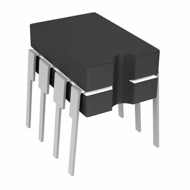
| 描述 | IC GATE DVR DUAL 2A 8-SOIC门驱动器 dual 2A with non-inverting TTL |
| 产品分类 | PMIC - MOSFET,电桥驱动器 - 外部开关集成电路 - IC |
| 品牌 | Fairchild Semiconductor |
| 产品手册 | |
| 产品图片 |
|
| rohs | 符合RoHS无铅 / 符合限制有害物质指令(RoHS)规范要求 |
| 产品系列 | 电源管理 IC,门驱动器,Fairchild Semiconductor FAN3227TMX- |
| 数据手册 | |
| 产品型号 | FAN3227TMX |
| PCN组件/产地 | |
| PCN设计/规格 | |
| 上升时间 | 12 ns |
| 下降时间 | 9 ns |
| 产品 | MOSFET Gate Drivers |
| 产品目录页面 | |
| 产品种类 | 门驱动器 |
| 供应商器件封装 | 8-SOIC |
| 其它名称 | FAN3227TMXCT |
| 包装 | 剪切带 (CT) |
| 单位重量 | 143 mg |
| 商标 | Fairchild Semiconductor |
| 安装类型 | 表面贴装 |
| 安装风格 | SMD/SMT |
| 封装 | Reel |
| 封装/外壳 | 8-SOIC(0.154",3.90mm 宽) |
| 封装/箱体 | SOIC-8 |
| 工作温度 | -40°C ~ 125°C |
| 工厂包装数量 | 2500 |
| 延迟时间 | 19ns |
| 最大功率耗散 | 0.46 W |
| 最大工作温度 | + 125 C |
| 最小工作温度 | - 40 C |
| 标准包装 | 1 |
| 激励器数量 | 2 Driver |
| 特色产品 | http://www.digikey.cn/product-highlights/cn/zh/fairchild-cloud-systems-computing/4301 |
| 电压-电源 | 4.5 V ~ 18 V |
| 电流-峰值 | 3A |
| 电源电压-最大 | 18 V |
| 电源电压-最小 | 4.5 V |
| 电源电流 | 0.75 mA |
| 类型 | Low-Side Driver |
| 系列 | FAN3227 |
| 输入类型 | 非反相 |
| 输出数 | 2 |
| 输出电流 | 3 A |
| 输出端数量 | 2 |
| 配置 | Non-Inverting |
| 配置数 | 2 |
| 高压侧电压-最大值(自举) | - |


- 商务部:美国ITC正式对集成电路等产品启动337调查
- 曝三星4nm工艺存在良率问题 高通将骁龙8 Gen1或转产台积电
- 太阳诱电将投资9.5亿元在常州建新厂生产MLCC 预计2023年完工
- 英特尔发布欧洲新工厂建设计划 深化IDM 2.0 战略
- 台积电先进制程称霸业界 有大客户加持明年业绩稳了
- 达到5530亿美元!SIA预计今年全球半导体销售额将创下新高
- 英特尔拟将自动驾驶子公司Mobileye上市 估值或超500亿美元
- 三星加码芯片和SET,合并消费电子和移动部门,撤换高东真等 CEO
- 三星电子宣布重大人事变动 还合并消费电子和移动部门
- 海关总署:前11个月进口集成电路产品价值2.52万亿元 增长14.8%


PDF Datasheet 数据手册内容提取
Is Now Part of To learn more about ON Semiconductor, please visit our website at www.onsemi.com Please note: As part of the Fairchild Semiconductor integration, some of the Fairchild orderable part numbers will need to change in order to meet ON Semiconductor’s system requirements. Since the ON Semiconductor product management systems do not have the ability to manage part nomenclature that utilizes an underscore (_), the underscore (_) in the Fairchild part numbers will be changed to a dash (-). This document may contain device numbers with an underscore (_). Please check the ON Semiconductor website to verify the updated device numbers. The most current and up-to-date ordering information can be found at www.onsemi.com. Please email any questions regarding the system integration to Fairchild_questions@onsemi.com. ON Semiconductor and the ON Semiconductor logo are trademarks of Semiconductor Components Industries, LLC dba ON Semiconductor or its subsidiaries in the United States and/or other countries. ON Semiconductor owns the rights to a number of patents, trademarks, copyrights, trade secrets, and other intellectual property. A listing of ON Semiconductor’s product/patent coverage may be accessed at www.onsemi.com/site/pdf/Patent-Marking.pdf. ON Semiconductor reserves the right to make changes without further notice to any products herein. ON Semiconductor makes no warranty, representation or guarantee regarding the suitability of its products for any particular purpose, nor does ON Semiconductor assume any liability arising out of the application or use of any product or circuit, and specifically disclaims any and all liability, including without limitation special, consequential or incidental damages. Buyer is responsible for its products and applications using ON Semiconductor products, including compliance with all laws, regulations and safety requirements or standards, regardless of any support or applications information provided by ON Semiconductor. “Typical” parameters which may be provided in ON Semiconductor data sheets and/or specifications can and do vary in different applications and actual performance may vary over time. All operating parameters, including “Typicals” must be validated for each customer application by customer’s technical experts. ON Semiconductor does not convey any license under its patent rights nor the rights of others. ON Semiconductor products are not designed, intended, or authorized for use as a critical component in life support systems or any FDA Class 3 medical devices or medical devices with a same or similar classification in a foreign jurisdiction or any devices intended for implantation in the human body. Should Buyer purchase or use ON Semiconductor products for any such unintended or unauthorized application, Buyer shall indemnify and hold ON Semiconductor and its officers, employees, subsidiaries, affiliates, and distributors harmless against all claims, costs, damages, and expenses, and reasonable attorney fees arising out of, directly or indirectly, any claim of personal injury or death associated with such unintended or unauthorized use, even if such claim alleges that ON Semiconductor was negligent regarding the design or manufacture of the part. ON Semiconductor is an Equal Opportunity/Affirmative Action Employer. This literature is subject to all applicable copyright laws and is not for resale in any manner.
F A N 3 2 April 2013 2 6 / F A N 3 FAN3226 / FAN3227 / FAN3228 / FAN3229 2 2 7 Dual 2-A High-Speed, Low-Side Gate Drivers / F A N Features 3 Description 2 2 Industry-Standard Pinouts 8 The FAN3226-29 family of dual 2 A gate drivers is / 4.5-V to 18-V Operating Range designed to drive N-channel enhancement-mode F A 3-A Peak Sink/Source at V = 12 V MOSFETs in low-side switching applications by N DD providing high peak current pulses during the short 3 2.4 A-Sink / 1.6-A Source at VOUT = 6 V switching intervals. The driver is available with either 2 2 Choice of TTL or CMOS Input Thresholds TTL or CMOS input thresholds. Internal circuitry 9 Four Versions of Dual Independent Drivers: pthreo vioduetsp uat nl ouwn duenr-tvil oltthaeg es ulopcpklyo uvt oflutangceti onis bwyi thhionl dtihneg — - Dual Inverting + Enable (FAN3226) operating range. In addition, the drivers feature matched D u - Dual Non-Inverting + Enable (FAN3227) internal propagation delays between A and B channels a - Dual Inputs in Two Pin-Out Configurations: ftoimr inagp,p liscuactiho nass resqyunicrihnrgo ndouuasl greactetif iedrrsiv.e sT hwisit he ncaribticleasl l 2- o Compatible with FAN3225x (FAN3228) connecting two drivers in parallel to effectively double A o Compatible with TPS2814D (FAN3229) the current capability driving a single MOSFET. Hi g Internal Resistors Turn Driver Off If No Inputs The FAN322X drivers incorporate MillerDrive™ h architecture for the final output stage. This bipolar- -S MillerDrive™ Technology MOSFET combination provides high current during the p e 12-ns / 9-ns Typical Rise/Fall Times (1-nF Load) Miller plateau stage of the MOSFET turn-on / turn-off e process to minimize switching loss, while providing rail- d Under 20-ns Typical Propagation Delay Matched , to-rail voltage swing and reverse current capability. L within 1 ns to the Other Channel o Double Current Capability by Paralleling Channels The FAN3226 offers two inverting drivers and the w FAN3227 offers two non-inverting drivers. Each device - 8-Lead 3x3 mm MLP or 8-Lead SOIC Package has dual independent enable pins that default to ON if Si d Rated from –40°C to +125°C Ambient not connected. In the FAN3228 and FAN3229, each e channel has dual inputs of opposite polarity, which G Automotive Qualified to AEC-Q100 (F085 Version) allows configuration as non-inverting or inverting with an a t optional enable function using the second input. If one e Applications or both inputs are left unconnected, internal resistors D bias the inputs such that the output is pulled low to hold r Switch-Mode Power Supplies iv the power MOSFET off. e High-Efficiency MOSFET Switching r s Synchronous Rectifier Circuits Related Resources DC-to-DC Converters AN-6069: Application Review and Comparative Motor Control Evaluation of Low-Side Gate Drivers Servers Automotive-Qualified Systems (F085 version) FAN3226 FAN3227 FAN3228 FAN3229 Figure 1. Pin Configurations © 2007 Fairchild Semiconductor Corporation www.fairchildsemi.com FAN3226 / FAN3227 / FAN3228 / FAN3229 • Rev. 1.1.0
F A N Ordering Information 3 2 2 Input Packing Quantity 6 Part Number Logic Package / Threshold Method per Reel F A FAN3226CMPX 3x3 mm MLP-8 Tape & Reel 3,000 N 3 FAN3226CMX CMOS SOIC-8 Tape & Reel 2,500 2 FAN3226CMX_F085(1) Dual Inverting Channels + Dual SOIC-8 Tape & Reel 2,500 27 FAN3226TMPX Enable 3x3 mm MLP-8 Tape & Reel 3,000 / F FAN3226TMX TTL SOIC-8 Tape & Reel 2,500 A FAN3226TMX_F085(1) SOIC-8 Tape & Reel 2,500 N3 2 FAN3227CMPX 3x3 mm MLP-8 Tape & Reel 3,000 2 FAN3227CMX CMOS SOIC-8 Tape & Reel 2,500 8 / FAN3227CMX_F085(1) Dual Non-Inverting Channels + SOIC-8 Tape & Reel 2,500 F A FAN3227TMPX Dual Enable 3x3 mm MLP-8 Tape & Reel 3,000 N FAN3227TMX TTL SOIC-8 Tape & Reel 2,500 3 2 FAN3227TMX_F085(1) SOIC-8 Tape & Reel 2,500 2 9 FAN3228CMX_F085(1) Dual Channels of Two-Input / CMOS SOIC-8 Tape & Reel 2,500 — One-Output Drivers, Pin FAN3228TMX_F085(1) Configuration 1 TTL SOIC-8 Tape & Reel 2,500 D u FAN3229CMPX 3x3 mm MLP-8 Tape & Reel 3,000 a FAN3229CMX CMOS SOIC-8 Tape & Reel 2,500 l 2 FAN3229CMX_F085(1) Dual Channels of Two-Input / SOIC-8 Tape & Reel 2,500 -A One-Output Drivers, Pin FAN3229TMPX Configuration 2 3x3 mm MLP-8 Tape & Reel 3,000 H i FAN3229TMX TTL SOIC-8 Tape & Reel 2,500 g h FAN3229TMX_F085(1) SOIC-8 Tape & Reel 2,500 - S p All standard Fairchild Semiconductor products are RoHS compliant and many are also “Green” or going green. Green means e the products are RoHS compliant AND they have limits on additional substances of Chlorine, Bromine and Antimony. For additional e information on Fairchild’s “green” Eco Status, please visit: http://www.fairchildsemi.com/company/green/rohs_green.html. d , Note: L 1. Qualified to AEC-Q100 o w - S i d e G a t e D r i v e r s © 2007 Fairchild Semiconductor Corporation www.fairchildsemi.com FAN3226 / FAN3227 / FAN3228 / FAN3229 • Rev. 1.1.0 2
F A N Package Outlines 3 2 2 6 / F A N 3 2 2 7 / F A N Figure 2. 3x3 mm MLP-8 (Top View) Figure 3. SOIC-8 (Top View) 3 2 2 8 / Thermal Characteristics(2) F A N Package ΘJL(3) ΘJT(4) ΘJA(5) ΨJB(6) ΨJT(7) Unit 3 2 8-Lead 3x3 mm Molded Leadless Package (MLP) 1.6 68 43 3.5 0.8 °C/W 2 9 8-Pin Small Outline Integrated Circuit (SOIC) 40 31 89 43 3.0 °C/W — Notes: D 2. Estimates derived from thermal simulation; actual values depend on the application. u 3. Theta_JL (ΘJL): Thermal resistance between the semiconductor junction and the bottom surface of all the leads (including any al thermal pad) that are typically soldered to a PCB. 2 4. Theta_JT (Θ ): Thermal resistance between the semiconductor junction and the top surface of the package, assuming it is -A JT held at a uniform temperature by a top-side heatsink. H 5. Theta_JA (ΘJA): Thermal resistance between junction and ambient, dependent on the PCB design, heat sinking, and airflow. ig The value given is for natural convection with no heatsink using a 2S2P board, as specified in JEDEC standards JESD51-2, h - JESD51-5, and JESD51-7, as appropriate. S 6. Psi_JB (Ψ ): Thermal characterization parameter providing correlation between semiconductor junction temperature and an p JB e application circuit board reference point for the thermal environment defined in Note 5. For the MLP-8 package, the board e reference is defined as the PCB copper connected to the thermal pad and protruding from either end of the package. For the d , SOIC-8 package, the board reference is defined as the PCB copper adjacent to pin 6. L 7. Psi_JT (Ψ ): Thermal characterization parameter providing correlation between the semiconductor junction temperature and o JT the center of the top of the package for the thermal environment defined in Note 5. w - S i d e G a t e D r i v e r s © 2007 Fairchild Semiconductor Corporation www.fairchildsemi.com FAN3226 / FAN3227 / FAN3228 / FAN3229 • Rev. 1.1.0 3
F A N 3 2 2 6 / F A N FAN3226 FAN3227 FAN3228 FAN3229 3 2 Figure 4. Pin Configurations (Repeated) 2 7 / Pin Definitions F A N Name Pin Description 3 2 Enable Input for Channel A. Pull pin LOW to inhibit driver A. ENA has TTL thresholds for both TTL and 2 ENA 8 CMOS INx threshold. / F ENB Enable Input for Channel B. Pull pin LOW to inhibit driver B. ENB has TTL thresholds for both TTL and A CMOS INx threshold. N 3 GND Ground. Common ground reference for input and output circuits. 2 2 9 INA Input to Channel A. — INA+ Non-Inverting Input to Channel A. Connect to VDD to enable output. D u INA- Inverting Input to Channel A. Connect to GND to enable output. a l INB Input to Channel B. 2 - A INB+ Non-Inverting Input to Channel B. Connect to VDD to enable output. H INB- Inverting Input to Channel B. Connect to GND to enable output. ig h OUTA Gate Drive Output A: Held LOW unless required input(s) are present and VDD is above UVLO threshold. -S p OUTB Gate Drive Output B: Held LOW unless required input(s) are present and VDD is above UVLO threshold. e e Gate Drive Output A (inverted from the input): Held LOW unless required input is present and V is d OUTA above UVLO threshold. DD , L o Gate Drive Output B (inverted from the input): Held LOW unless required input is present and V is w DD OUTB above UVLO threshold. -S i d Thermal Pad (MLP only). Exposed metal on the bottom of the package; may be left floating or connected P1 e to GND; NOT suitable for carrying current. G a VDD Supply Voltage. Provides power to the IC. t e D r i Output Logic v e r s FAN3228 and FAN3229 FAN3226 (x=A or B) FAN3227 (x=A or B) (x=A or B) ENx INx OUTx ENx INx OUTx INx+ INx− OUTx 0 0 0 0 0(8) 0 0(8) 0 0 0 1(8) 0 0 1 0 0(8) 1(8) 0 1(8) 0 1 1(8) 0(8) 0 1 0 1 1(8) 1(8) 0 1(8) 1 1 1 1(8) 0 Note: 8. Default input signal if no external connection is made. © 2007 Fairchild Semiconductor Corporation www.fairchildsemi.com FAN3226 / FAN3227 / FAN3228 / FAN3229 • Rev. 1.1.0 4
F Block Diagrams A N 3 2 2 V V 6 DD DD / F 100k 100k A ENA 1 8 ENB N 3 2 V 2 DD 7 / 100k F A INA 2 OUTA N 7 3 2 100k 2 8 / GND 3 F UVLO 6 VDD A N 3 V 2 V DD_OK 2 DD 9 — 100k OUTB D 5 INB 4 u a 100k l 2 - A H i g Figure 5. FAN3226 Block Diagram h - S p e e d , L o w - S i d e G a t e D r i v e r s Figure 6. FAN3227 Block Diagram © 2007 Fairchild Semiconductor Corporation www.fairchildsemi.com FAN3226 / FAN3227 / FAN3228 / FAN3229 • Rev. 1.1.0 5
F Block Diagrams A N 3 2 2 6 / F A N 3 2 2 7 / F A N 3 2 2 8 / F A N 3 2 2 9 — D u a l 2 - A H i g h - Figure 7. FAN3228 Block Diagram S p e e d , L o w - S i d e G a t e D r i v e r s Figure 8. FAN3229 Block Diagram © 2007 Fairchild Semiconductor Corporation www.fairchildsemi.com FAN3226 / FAN3227 / FAN3228 / FAN3229 • Rev. 1.1.0 6
F A Absolute Maximum Ratings N 3 Stresses exceeding the absolute maximum ratings may damage the device. The device may not function or be 2 2 operable above the recommended operating conditions and stressing the parts to these levels is not recommended. 6 In addition, extended exposure to stresses above the recommended operating conditions may affect device reliability. / F The absolute maximum ratings are stress ratings only. A N Symbol Parameter Min. Max. Unit 3 2 2 V VDD to PGND -0.3 20.0 V DD 7 / VEN ENA and ENB to GND GND - 0.3 VDD + 0.3 V F A VIN INA, INA+, INA–, INB, INB+ and INB– to GND GND - 0.3 VDD + 0.3 V N 3 VOUT OUTA and OUTB to GND GND - 0.3 VDD + 0.3 V 2 2 T Lead Soldering Temperature (10 Seconds) +260 ºC 8 L / F T Junction Temperature -55 +150 ºC J A N T Storage Temperature -65 +150 ºC STG 3 2 2 9 — Recommended Operating Conditions D u a The Recommended Operating Conditions table defines the conditions for actual device operation. Recommended l operating conditions are specified to ensure optimal performance to the datasheet specifications. Fairchild does not 2 - recommend exceeding them or designing to Absolute Maximum Ratings. A H Symbol Parameter Min. Max. Unit ig h VDD Supply Voltage Range 4.5 18.0 V -S p VEN Enable Voltage ENA and ENB 0 VDD V e e V Input Voltage INA, INA+, INA–, INB, INB+ and INB– 0 V V d IN DD , L TA Operating Ambient Temperature -40 +125 ºC o w - S i d e G a t e D r i v e r s © 2007 Fairchild Semiconductor Corporation www.fairchildsemi.com FAN3226 / FAN3227 / FAN3228 / FAN3229 • Rev. 1.1.0 7
F A Electrical Characteristics N 3 Unless otherwise noted, V =12 V, T =-40°C to +125°C. Currents are defined as positive into the device and 2 DD J 2 negative out of the device. 6 / Symbol Parameter Conditions Min. Typ. Max. Unit F A Supply N 3 V Operating Range 4.5 18.0 V 2 DD 2 Supply Current Inputs / EN TTL 0.75 1.20 mA 7 IDD Not Connected CMOS(9) 0.65 1.05 mA / F A V Turn-On Voltage INA=ENA=V , INB=ENB=0 V 3.5 3.9 4.3 V N ON DD 3 VOFF Turn-Off Voltage INA=ENA=VDD, INB=ENB=0 V 3.3 3.7 4.1 V 2 2 FAN322xCMX_F085, FAN322xTMX_F085 (Automotive-Qualified Versions) 8 / VON Turn-On Voltage(14) INA=ENA=VDD, INB=ENB=0 V 3.3 3.9 4.5 V F A VOFF Turn-Off Voltage(14) INA=ENA=VDD, INB=ENB=0 V 3.1 3.7 4.3 V N Inputs (FAN322xT)(10) 32 2 VINL_T INx Logic Low Threshold 0.8 1.2 V 9 — V INx Logic High Threshold 1.6 2.0 V INH_T D V TTL Logic Hysteresis Voltage 0.2 0.4 0.8 V HYS_T u FAN322xT a l 2 IIN+ Non-Inverting Input Current IN from 0 to VDD -1 175 µA - A IIN- Inverting Input Current IN from 0 to VDD -175 1 µA H FAN322xTMX_F085 (Automotive-Qualified Versions) ig h IINx_T Non-inverting Input Current(14) IN=0 V -1.5 1.5 µA -S I Non-inverting Input Current(14) IN=V 90 120 175.0 µA p INx_T DD e I Inverting Input Current(14) IN=0 V -175 -120 -90 µA e INx_T d I Inverting Input Current(14) IN=V -1.5 1.5 µA , INx_T DD L Inputs (FAN322xC)(10) o w VINL_C INx Logic Low Threshold 30 38 %VDD -S i V INx Logic High Threshold 55 70 %V d INH_C DD e VHYS_C CMOS Logic Hysteresis Voltage 17 %VDD G a FAN322xC t e IIN+ Non-Inverting Input Current IN from 0 to VDD -1 175 µA D r IIN- Inverting Input Current IN from 0 to VDD -175 1 µA iv e FAN322xCMX_F085 (Automotive-Qualified Versions) r s I Non-inverting Input Current(14) IN=0 V -1.5 1.5 µA INx_T I Non-inverting Input Current(14) IN=V 90 120 175.0 µA INx_T DD I Inverting Input Current(14) IN=0 V -175 -120 -90 µA INx_T I Inverting Input Current(14) IN=V -1.5 1.5 µA INx_T DD ENABLE (FAN3226C, FAN3226T, FAN3227C, FAN3227T) V Enable Logic Low Threshold EN from 5 V to 0 V 0.8 1.2 V ENL V Enable Logic High Threshold EN from 0 V to 5 V 1.6 2.0 V ENH V TTL Logic Hysteresis Voltage(11) 0.4 V HYS_T R Enable Pull-up Resistance(11) 100 kΩ PU Continued on the following page… © 2007 Fairchild Semiconductor Corporation www.fairchildsemi.com FAN3226 / FAN3227 / FAN3228 / FAN3229 • Rev. 1.1.0 8
F A Electrical Characteristics (Continued) N 3 Unless otherwise noted, V =12 V, T =-40°C to +125°C. Currents are defined as positive into the device and 2 DD J 2 negative out of the device. 6 / F Symbol Parameter Conditions Min. Typ. Max. Unit A N ENABLE (FAN3226C, FAN3226T, FAN3227C, FAN3227T) (continued) 3 2 t 0 V to 5 V EN, 1 V/ns Slew Rate 10 19 34 ns 2 D3 EN to Output Propagation Delay(12) 7 t 5 V to 0 V EN, 1 V/ns Slew Rate 10 18 32 ns / D4 F FAN3226CMX, FAN3226TMX, FAN3227CMX, FAN3227TMX_F085 (Automotive-Qualified Versions) A N t 0 V to 5 V EN, 1 V/ns Slew Rate 8 19 35 ns 3 D3 EN to Output Propagation Delay(12),(14) 22 tD4 5 V to 0 V EN, 1 V/ns Slew Rate 8 18 35 ns 8 / Outputs F A OUT at V /2, N I OUT Current, Mid-Voltage, Sinking(11) DD 2.4 A SINK C =0.1 µF, f=1 kHz 3 LOAD 2 2 ISOURCE OSoUuTrc Cinugr(r1e1n) t, Mid-Voltage, OCLUOTAD a=t0 V.1D Dµ/F2,, f=1 kHz -1.6 A 9 — I OUT Current, Peak, Sinking(11) C =0.1 µF, f=1 kHz 3 A D PK_SINK LOAD u IPK_SOURCE OUT Current, Peak, Sourcing(11) CLOAD=0.1 µF, f=1 kHz -3 A al tRISE Output Rise Time(13) CLOAD=1000 pF 12 22 ns 2-A tFALL Output Fall Time(13) CLOAD=1000 pF 9 17 ns H i I Output Reverse Current Withstand(11) 500 mA g RVS h - FAN322xT, FAN322xC S p e tD1 Output Propagation Delay, CMOS CMOS Input 7 15 30 e Inputs(13) ns d t CMOS Input 6 15 29 , D2 L tD1 Output Propagation Delay, TTL TTL Input 10 19 34 ow ns tD2 Inputs(13) TTL Input 10 18 32 -S i d t Propagation Matching Between INA=INB, OUTA and OUTB at 1 2 ns e DEL.MATCH Channels(14) 50% Point G a FAN322xTMX_F085, FAN322xCMX_F085 (Automotive-Qualified Versions) t e tD1 Output Propagation Delay, CMOS CMOS Input 7 15 33 D ns r t Inputs(13),(14) CMOS Input 6 15 42 iv D2 e r tD1 Output Propagation Delay, TTL TTL Input 9 19 34 s ns Inputs(13),(14) t TTL Input 9 18 32 D2 Propagation Matching Between INA=INB, OUTA and OUTB at t 2 4 ns DEL.MATCH Channels(14) 50% Point VOH High Level Output Voltage(14) VOH =VDD–VOUT, IOUT=–1 mA 15 35 mV V Low Level Output Voltage(14) I = 1 mA 10 25 mV OL OUT Notes: 9. Lower supply current due to inactive TTL circuitry. 10. EN inputs have TTL thresholds; refer to the ENABLE section. 11. Not tested in production. 12. See Timing Diagrams of Figure 11 and Figure 12. 13. See Timing Diagrams of Figure 9 and Figure 10. 14. Apply to only F085 Version © 2007 Fairchild Semiconductor Corporation www.fairchildsemi.com FAN3226 / FAN3227 / FAN3228 / FAN3229 • Rev. 1.1.0 9
F Timing Diagrams A N 3 2 2 6 / F 90% 90% A N Output Output 3 2 2 10% 10% 7 / F A V INH V N Input INH VINL Input V 322 INL 8 tD1 tD2 tD1 tD2 / F A N t t t t 3 RISE FALL FALL RISE 2 2 9 Figure 9. Non-Inverting (EN HIGH or Floating) Figure 10. Inverting (EN HIGH or Floating) — D u a l 2 - A H i g h - S p e e d , L o w - S i d e G a t e D r i v e r s Figure 11. Non-Inverting (IN HIGH) Figure 12. Inverting (IN LOW) © 2007 Fairchild Semiconductor Corporation www.fairchildsemi.com FAN3226 / FAN3227 / FAN3228 / FAN3229 • Rev. 1.1.0 10
F A N Typical Performance Characteristics 3 2 2 Typical characteristics are provided at 25°C and V =12 V unless otherwise noted. 6 DD / F 1.6 1.6 A N 1.4 FAN3226C, 27C 1.4 TTL Input 3 1.2 1.2 2 2 mA) 01..80 mA) 01..80 7 / F I (DD0.6 I (DD 0.6 AN 0.4 Inputs and Enables 0.4 Inputs and Enables 32 0.2 Floating, Outputs 0.2 Floating, Outputs Low 2 8 0.0 0.0 / 4 6 8 10 12 14 16 18 4 6 8 10 12 14 16 18 F A Supply Voltage (V) Supply Voltage (V) N 3 2 2 Figure 13. IDD (Static) vs. Supply Voltage(15) Figure 14. IDD (Static) vs. Supply Voltage(15) 9 — 1.6 D u 1.4 FAN3228C, 29C a l 1.2 2 - 1.0 A mA) 0.8 All Inputs Floating, H (D Outputs Low ig D0.6 h I - 0.4 S p 0.2 e e 0.0 d , 4 6 8 10 12 14 16 18 L V - Supply Voltage (V) o DD w Figure 15.IDD(Static) vs. Supply Voltage(15) -S i d e G a t e D r i v e r s Figure 16. I (No-Load) vs. Frequency Figure 17. I (No-Load) vs. Frequency DD DD © 2007 Fairchild Semiconductor Corporation www.fairchildsemi.com FAN3226 / FAN3227 / FAN3228 / FAN3229 • Rev. 1.1.0 11
F A Typical Performance Characteristics N 3 Typical characteristics are provided at 25°C and V =12 V unless otherwise noted. 2 DD 2 6 / F A N 3 2 2 7 / F A N 3 2 2 8 / F A N 3 2 2 9 Figure 18. IDD (1 nF Load) vs. Frequency Figure 19. IDD (1 nF Load) vs. Frequency — D u 1.6 1.6 a 1.4 FAN3226C, 27C 1.4 TTL Input l 2 - A 1.2 1.2 H A) 1.0 A)1.0 ig m 0.8 m0.8 h I (DD0.6 (DD0.6 -Sp I e 0.4 Inputs and Enables 0.4 Inputs and Enables e d 0.2 Floating, Outputs 0.2 Floating, Outputs , L 0.0 0.0 o w -50 -25 0 25 50 75 100 125 -50 -25 0 25 50 75 100 125 - S Temperature (°C) Temperature (°C) i d e G Figure 20. IDD (Static) vs. Temperature(15) Figure 21. IDD (Static) vs. Temperature(15) a t e D 1.6 r i v 1.4 FAN3228C,29C e r s 1.2 1.0 ) A m 0.8 ( D ID0.6 0.4 AllInputsFloating, 0.2 OutputsLow 0.0 -50 -25 0 25 50 75 100 125 Temperature (°C) Figure 22.I (Static) vs. Temperature(15) DD © 2007 Fairchild Semiconductor Corporation www.fairchildsemi.com FAN3226 / FAN3227 / FAN3228 / FAN3229 • Rev. 1.1.0 12
F A Typical Performance Characteristics N 3 Typical characteristics are provided at 25°C and V =12 V unless otherwise noted. 2 DD 2 6 / F A N 3 2 2 7 / F A N 3 2 2 8 / F A N 3 2 2 9 Figure 23. Input Thresholds vs. Supply Voltage Figure 24. Input Thresholds vs. Supply Voltage — D u a l 2 - A H i g h - S p e e d , L o w - S i d e G Figure 25. Input Threshold % vs. Supply Voltage a t e D r i v e r s Figure 26. Input Thresholds vs. Temperature Figure 27. Input Thresholds vs. Temperature © 2007 Fairchild Semiconductor Corporation www.fairchildsemi.com FAN3226 / FAN3227 / FAN3228 / FAN3229 • Rev. 1.1.0 13
F A Typical Performance Characteristics N 3 Typical characteristics are provided at 25°C and V =12 V unless otherwise noted. 2 DD 2 6 / F A N 3 2 2 7 / F A N 3 2 2 8 / F A N 3 2 2 9 Figure 28. UVLO Thresholds vs. Temperature Figure 29. UVLO Threshold vs. Temperature — D u a l 2 - A H i g h - S p e e d , L o w - S id e Figure 30. Propagation Delays vs. Supply Voltage Figure 31. Propagation Delays vs. Supply Voltage G a t e D r i v e r s Figure 32. Propagation Delays vs. Supply Voltage Figure 33. Propagation Delays vs. Supply Voltage © 2007 Fairchild Semiconductor Corporation www.fairchildsemi.com FAN3226 / FAN3227 / FAN3228 / FAN3229 • Rev. 1.1.0 14
F A Typical Performance Characteristics N 3 Typical characteristics are provided at 25°C and V =12 V unless otherwise noted. 2 DD 2 6 / F A N 3 2 2 7 / F A N 3 2 2 8 / F A N 3 2 2 9 Figure 34. Propagation Delays vs. Temperature Figure 35. Propagation Delays vs. Temperature — D u a l 2 - A H i g h - S p e e d , L o w - S i d e G Figure 36. Propagation Delays vs. Temperature Figure 37. Propagation Delays vs. Temperature a t e D r i v e r s Figure 38. Fall Time vs. Supply Voltage Figure 39. Rise Time vs. Supply Voltage © 2007 Fairchild Semiconductor Corporation www.fairchildsemi.com FAN3226 / FAN3227 / FAN3228 / FAN3229 • Rev. 1.1.0 15
F A Typical Performance Characteristics N 3 Typical characteristics are provided at 25°C and V =12 V unless otherwise noted. 2 DD 2 6 / F A N 3 2 2 7 / F A N 3 2 2 8 / F A N 3 2 2 Figure 40.Rise and Fall Times vs. Temperature 9 — D u a l 2 - A H i g h - S p e e d , L o w - S i Figure 41. Rise/Fall Waveforms with 1 nF Load Figure 42. Rise/Fall Waveforms with 10 nF Load d e G a t e D r i v e r s Figure 43. Quasi-Static Source Current with V =12 V Figure 44. Quasi-Static Sink Current with V =12 V DD DD © 2007 Fairchild Semiconductor Corporation www.fairchildsemi.com FAN3226 / FAN3227 / FAN3228 / FAN3229 • Rev. 1.1.0 16
F A Typical Performance Characteristics N 3 Typical characteristics are provided at 25°C and V =12 V unless otherwise noted. 2 DD 2 6 / F A N 3 2 2 7 / F A N 3 2 2 8 / F A N 3 2 2 9 Figure 45. Quasi-Static Source Current with V =8 V Figure 46. Quasi-Static Sink Current with V =8 V DD DD — D Note: u 15. For any inverting inputs pulled low, non-inverting inputs pulled high, or outputs driven high, static I increases by a DD l the current flowing through the corresponding pull-up/down resistor shown in the block diagram. 2 -A H Test Circuit i g h - S p e e d , L o w - S i d e G a t e D r i v e r s Figure 47.Quasi-Static IOUT/ VOUTTest Circuit © 2007 Fairchild Semiconductor Corporation www.fairchildsemi.com FAN3226 / FAN3227 / FAN3228 / FAN3229 • Rev. 1.1.0 17
F A N Applications Information 3 2 Input Thresholds MillerDrive™ Gate Drive Technology 26 Each member of the FAN322x driver family consists of FAN322x gate drivers incorporate the MillerDrive™ / F two identical channels that may be used independently architecture shown in Figure 48. For the output stage, a A at rated current or connected in parallel to double the combination of bipolar and MOS devices provide large N individual current capacity. In the FAN3226 and currents over a wide range of supply voltage and 32 FAN3227, channels A and B can be enabled or disabled temperature variations. The bipolar devices carry the 2 independently using ENA or ENB, respectively. The EN bulk of the current as OUT swings between 1/3 to 2/3 7 pin has TTL thresholds for parts with either CMOS or VDD and the MOS devices pull the output to the high or / F TTL input thresholds. If ENA and ENB are not low rail. A connected, an internal pull-up resistor enables the driver The purpose of the MillerDrive™ architecture is to N3 channels by default. If the channel A and channel B speed up switching by providing high current during the 2 inputs and outputs are connected in parallel to increase Miller plateau region when the gate-drain capacitance of 28 the driver current capacity, ENA and ENB should be the MOSFET is being charged or discharged as part of / connected and driven together. the turn-on / turn-off process. F A The FAN322x family offers versions in either TTL or For applications that have zero voltage switching during N CMOS input thresholds. In the FAN322xT, the input 3 the MOSFET turn-on or turn-off interval, the driver 2 thresholds meet industry-standard TTL-logic thresholds supplies high peak current for fast switching even 2 independent of the VDD voltage, and there is a though the Miller plateau is not present. This situation 9 hysteresis voltage of approximately 0.4 V. These levels often occurs in synchronous rectifier applications — permit the inputs to be driven from a range of input logic because the body diode is generally conducting before D signal levels for which a voltage over 2 V is considered the MOSFET is switched on. u logic high. The driving signal for the TTL inputs should a l have fast rising and falling edges with a slew rate of The output pin slew rate is determined by VDD voltage 2 6 V/µs or faster, so a rise time from 0 to 3.3 V should be and the load on the output. It is not user adjustable, but -A 550 ns or less. With reduced slew rate, circuit noise a series resistor can be added if a slower rise or fall time H could cause the driver input voltage to exceed the at the MOSFET gate is needed. i g hysteresis voltage and retrigger the driver input, causing h erratic operation. - S p In the FAN322xC, the logic input thresholds are e dependent on the V level and, with V of 12 V, the e DD DD d logic rising edge threshold is approximately 55% of VDD , and the input falling edge threshold is approximately L o 38% of VDD. The CMOS input configuration offers a w hysteresis voltage of approximately 17% of VDD. The -S CMOS inputs can be used with relatively slow edges i d (approaching DC) if good decoupling and bypass e techniques are incorporated in the system design to G prevent noise from violating the input voltage hysteresis a window. This allows setting precise timing intervals by te fitting an R-C circuit between the controlling signal and D the IN pin of the driver. The slow rising edge at the IN r i pin of the driver introduces a delay between the Figure 48. MillerDrive™ Output Architecture v e controlling signal and the OUT pin of the driver. r Under-Voltage Lockout s Static Supply Current The FAN322x startup logic is optimized to drive ground- In the I (static) typical performance characteristics referenced N-channel MOSFETs with an under-voltage DD (see Figure 13 - Figure 15 and Figure 20 - Figure 22), lockout (UVLO) function to ensure that the IC starts up the curve is produced with all inputs / enables floating in an orderly fashion. When VDD is rising, yet below the (OUT is low) and indicates the lowest static I current 3.9 V operational level, this circuit holds the output low, DD for the tested configuration. For other states, additional regardless of the status of the input pins. After the part current flows through the 100 kΩ resistors on the inputs is active, the supply voltage must drop 0.2 V before the and outputs shown in the block diagram of each part part shuts down. This hysteresis helps prevent chatter (see Figure 5 - Figure 8). In these cases, the actual when low VDD supply voltages have noise from the static I current is the value obtained from the curves power switching. This configuration is not suitable for DD plus this additional current. driving high-side P-channel MOSFETs because the low output voltage of the driver would turn the P-channel MOSFET on with V below 3.9 V. DD © 2007 Fairchild Semiconductor Corporation www.fairchildsemi.com FAN3226 / FAN3227 / FAN3228 / FAN3229 • Rev. 1.1.0 18
F A V Bypass Capacitor Guidelines DD N To enable this IC to turn a device on quickly, a local high- best results, make connections to all pins as short 3 2 frequency bypass capacitor CBYP with low ESR and ESL and direct as possible. 2 should be connected between the VDD and GND pins The FAN322x is compatible with many other 6 / with minimal trace length. This capacitor is in addition to industry-standard drivers. In single input parts with F bulk electrolytic capacitance of 10 µF to 47 µF commonly A enable pins, there is an internal 100 kΩ resistor tied found on driver and controller bias circuits. N to VDD to enable the driver by default; this should be 3 A typical criterion for choosing the value of C is to considered in the PCB layout. 2 BYP 2 kise eopft etnh ea crihpipelvee dvo wltaitghe a o vna ltuhee ≥V2D0D tsimupepsl yt hteo e≤q5u%iv. aTlehnist The turn-on and turn-off current paths should be 7 / minimized, as discussed in the following section. F load capacitance C , defined here as Q /V . EQV GATE DD A Ceramic capacitors of 0.1 µF to 1 µF or larger are Figure 49 shows the pulsed gate drive current path N common choices, as are dielectrics, such as X5R and when the gate driver is supplying gate charge to turn the 3 X7R with good temperature characteristics and high MOSFET on. The current is supplied from the local 2 2 pulse current capability. bypass capacitor, CBYP, and flows through the driver to 8 the MOSFET gate and to ground. To reach the high / If circuit noise affects normal operation, the value of peak currents possible, the resistance and inductance in F CBYP may be increased to 50-100 times the CEQV, or the path should be minimized. The localized CBYP acts AN CBYP may be split into two capacitors. One should be a to contain the high peak current pulses within this driver- 3 larger value, based on equivalent load capacitance, and MOSFET circuit, preventing them from disturbing the 2 2 the other a smaller value, such as 1-10 nF mounted sensitive analog circuitry in the PWM controller. 9 closest to the VDD and GND pins to carry the higher — frequency components of the current pulses. The V V bypass capacitor must provide the pulsed current from DD DS D u both of the driver channels and, if the drivers are a switching simultaneously, the combined peak current l C 2 sourced from the CBYP would be twice as large as when BYP - A a single channel is switching. H Layout and Connection Guidelines i FAN322x g h The FAN3226-26 family of gate drivers incorporates - S fast-reacting input circuits, short propagation delays, p and powerful output stages capable of delivering current PWM e peaks over 2 A to facilitate voltage transition times from e d under 10 ns to over 150 ns. The following layout and , connection guidelines are strongly recommended: L o Figure 49. Current Path for MOSFET Turn-on w Keep high-current output and power ground paths - S separate logic and enable input signals and signal Figure 50 shows the current path when the gate driver i ground paths. This is especially critical when turns the MOSFET off. Ideally, the driver shunts the d e dealing with TTL-level logic thresholds at driver current directly to the source of the MOSFET in a small G inputs and enable pins. circuit loop. For fast turn-off times, the resistance and a Keep the driver as close to the load as possible to inductance in this path should be minimized. te minimize the length of high-current traces. This D V V r reduces the series inductance to improve high- DD DS i v speed switching, while reducing the loop area that e can radiate EMI to the driver inputs and rs surrounding circuitry. C BYP If the inputs to a channel are not externally FAN322x connected, the internal 100 kΩ resistors indicated on block diagrams command a low output. In noisy environments, it may be necessary to tie inputs of an unused channel to VDD or GND using short traces to prevent noise from causing spurious PWM output switching. Many high-speed power circuits can be susceptible to noise injected from their own output or other Figure 50. Current Path for MOSFET Turn-off external sources, possibly causing output re- triggering. These effects can be obvious if the circuit is tested in breadboard or non-optimal circuit layouts with long input, enable, or output leads. For © 2007 Fairchild Semiconductor Corporation www.fairchildsemi.com FAN3226 / FAN3227 / FAN3228 / FAN3229 • Rev. 1.1.0 19
F Truth Table of Logic Operation Operational Waveforms A N The FAN3228/FAN3229 truth table indicates the At power-up, the driver output remains low until the VDD 3 operational states using the dual-input configuration. In voltage reaches the turn-on threshold. The magnitude of 2 2 a non-inverting driver configuration, the IN- pin should the OUT pulses rises with V until steady-state V is 6 DD DD be a logic low signal. If the IN- pin is connected to logic reached. The non-inverting operation illustrated in / F high, a disable function is realized, and the driver output Figure 53 shows that the output remains low until the A remains low regardless of the state of the IN+ pin. UVLO threshold is reached, the output is in-phase with N the input. 3 IN+ IN- OUT 2 2 7 0 0 0 / 0 1 0 F A 1 0 1 N 3 1 1 0 2 2 8 / In the non-inverting driver configuration in Figure 51, the F IN- pin is tied to ground and the input signal (PWM) is A N applied to IN+ pin. The IN- pin can be connected to logic 3 high to disable the driver and the output remains low, 2 regardless of the state of the IN+ pin. 2 9 — VDD D u a IN+ l PWM 2 - OUT A FAN3228/9 IN- H i g Figure 53. Non-Inverting Startup Waveforms h - GND S For the inverting configuration of Figure 52, startup p waveforms are shown in Figure 54. With IN+ tied to V e DD e and the input signal applied to IN–, the OUT pulses are d inverted with respect to the input. At power-up, the , L inverted output remains low until the VDD voltage o reaches the turn-on threshold, then it follows the input w Figure 51. Dual-Input Driver Enabled, with inverted phase. -S Non-Inverting Configuration id e In the inverting driver application in Figure 52, the IN+ G pin is tied high. Pulling the IN+ pin to GND forces the a output low, regardless of the state of the IN- pin. te D r i v e r s Figure 52. Dual-Input Driver Enabled, Inverting Configuration Figure 54. Inverting Startup Waveforms © 2007 Fairchild Semiconductor Corporation www.fairchildsemi.com FAN3226 / FAN3227 / FAN3228 / FAN3229 • Rev. 1.1.0 20
F Thermal Guidelines A N Gate drivers used to switch MOSFETs and IGBTs at In the forward converter with synchronous rectifier 3 high frequencies can dissipate significant amounts of shown in the typical application diagrams, the 2 2 power. It is important to determine the driver power FDMS8660S is a reasonable MOSFET selection. The 6 dissipation and the resulting junction temperature in the gate charge for each SR MOSFET would be 60 nC with / F application to ensure that the part is operating within V = V = 7V. At a switching frequency of 500 kHz, GS DD A acceptable temperature limits. the total power dissipation is: N 3 The total power dissipation in a gate driver is the sum of PGATE = 60 nC • 7 V • 500 kHz • 2 = 0.42 W (5) 2 two components, P and P : 2 GATE DYNAMIC P = 3 mA • 7 V • 2 = 0.042 W (6) 7 DYNAMIC PTOTAL = PGATE + PDYNAMIC (1) P = 0.46 W (7) / F TOTAL A Gate Driving Loss: The most significant power loss The SOIC-8 has a junction-to-board thermal N rtiemseu)lt sto f rsowmit cshu pthpely ilnoga dg aMteO cSuFrEreTn to (nc haanrdg eo fpf eart uthneit characterization parameter of ψJB = 43°C/W. In a 32 switching frequency. The power dissipation that system application, the localized temperature around 28 results from driving a MOSFET at a specified gate- the device is a function of the layout and construction of / source voltage, V , with gate charge, Q , at the PCB along with airflow across the surfaces. To F switching frequencyG, Sf , is determined by: G ensure reliable operation, the maximum junction A SW N temperature of the device must be prevented from 3 PGATE = QG • VGS • fSW • n (2) exceeding the maximum rating of 150°C; with 80% 2 derating, T would be limited to 120°C. Rearranging 2 n is the number of driver channels in use (1 or 2). J 9 Equation 4 determines the board temperature required — Dynamic Pre-drive / Shoot-through Current: A to maintain the junction temperature below 120°C: power loss resulting from internal current D consumption under dynamic operating conditions, TB = TJ - PTOTAL • ψJB (8) u a including pin pull-up / pull-down resistors, can be l T = 120°C – 0.46 W • 43°C/W = 100°C (9) B 2 obtained using the “I (No-Load) vs. Frequency” DD - graphs in Typical Performance Characteristics to For comparison, replace the SOIC-8 used in the A determine the current I drawn from V previous example with the 3x3 mm MLP package with H DYNAMIC DD under actual operating conditions: ψ = 3.5°C/W. The 3x3 mm MLP package could ig JB h operate at a PCB temperature of 118°C, while PDYNAMIC = IDYNAMIC • VDD • n (3) maintaining the junction temperature below 120°C. This -S p Once the power dissipated in the driver is determined, illustrates that the physically smaller MLP package with e the driver junction rise with respect to circuit board can thermal pad offers a more conductive path to remove e d be evaluated using the following thermal equation, the heat from the driver. Consider tradeoffs between , assuming ψ was determined for a similar thermal reducing overall circuit size with junction temperature L JB o design (heat sinking and air flow): reduction for increased reliability. w - T = P • ψ + T (4) S J TOTAL JB B i d where: e TJ = driver junction temperature G ψJB = (psi) thermal characterization parameter ate relating temperature rise to total power D dissipation r TB = board temperature in location defined in Note iv 2 under Thermal Resistance table. e r s © 2007 Fairchild Semiconductor Corporation www.fairchildsemi.com FAN3226 / FAN3227 / FAN3228 / FAN3229 • Rev. 1.1.0 21
F A Typical Application Diagrams N 3 2 2 6 / F A N 3 2 2 7 / F A N 3 2 2 8 / F A N 3 2 2 Figure 55. Forward Converter Figure 56. Primary-Side Dual Driver 9 with Synchronous Rectification in a Push-Pull Converter — D u a l 2 - A H i g h - S p e e d , L o w - S i d e G a t e D r i v e r s Figure 57. Phase-Shifted Full-Bridge with Two Gate Drive Transformers (Simplified) © 2007 Fairchild Semiconductor Corporation www.fairchildsemi.com FAN3226 / FAN3227 / FAN3228 / FAN3229 • Rev. 1.1.0 22
F Table 1. Related Products A N 3 Part Gate Drive(16) Input 2 Type Logic Package 2 Number (Sink/Src) Threshold 6 / Single 1 A FAN3111C +1.1 A / -0.9 A CMOS Single Channel of Dual-Input/Single-Output SOT23-5, MLP6 F A Single 1 A FAN3111E +1.1 A / -0.9 A External(17) Single Non-Inverting Channel with External Reference SOT23-5, MLP6 N 3 2 Single 2 A FAN3100C +2.5 A / -1.8 A CMOS Single Channel of Two-Input/One-Output SOT23-5, MLP6 2 7 Single 2 A FAN3100T +2.5 A / -1.8 A TTL Single Channel of Two-Input/One-Output SOT23-5, MLP6 / F Single 2 A FAN3180 +2.4 A / -1.6 A TTL Single Non-Inverting Channel + 3.3-V LDO SOT23-5 A N 3 Dual 2 A FAN3216T +2.4 A / -1.6 A TTL Dual Inverting Channels SOIC8 2 2 Dual 2 A FAN3217T +2.4 A / -1.6 A TTL Dual Non-Inverting Channels SOIC8 8 / Dual 2 A FAN3226C +2.4 A / -1.6 A CMOS Dual Inverting Channels + Dual Enable SOIC8, MLP8 F A N Dual 2 A FAN3226T +2.4 A / -1.6 A TTL Dual Inverting Channels + Dual Enable SOIC8, MLP8 3 2 Dual 2 A FAN3227C +2.4 A / -1.6 A CMOS Dual Non-Inverting Channels + Dual Enable SOIC8, MLP8 2 9 Dual 2 A FAN3227T +2.4 A / -1.6 A TTL Dual Non-Inverting Channels + Dual Enable SOIC8, MLP8 — Dual 2 A FAN3228C +2.4 A / -1.6 A CMOS Dual Channels of Two-Input/One-Output, Pin Config.1 SOIC8, MLP8 D u a Dual 2 A FAN3228T +2.4 A / -1.6 A TTL Dual Channels of Two-Input/One-Output, Pin Config.1 SOIC8, MLP8 l 2 Dual 2 A FAN3229C +2.4 A / -1.6 A CMOS Dual Channels of Two-Input/One-Output, Pin Config.2 SOIC8, MLP8 -A H Dual 2 A FAN3229T +2.4 A / -1.6 A TTL Dual Channels of Two-Input/One-Output, Pin Config.2 SOIC8, MLP8 i g 20 V Non-Inverting Channel (NMOS) and Inverting h Dual 2 A FAN3268T +2.4 A / -1.6 A TTL SOIC8 - Channel (PMOS) + Dual Enables S p 30 V Non-Inverting Channel (NMOS) and Inverting e Dual 2 A FAN3278T +2.4 A / -1.6 A TTL SOIC8 e Channel (PMOS) + Dual Enables d , Dual 4 A FAN3213T +2.5 A / -1.8 A TTL Dual Inverting Channels SOIC8 L o w Dual 4 A FAN3214T +2.5 A / -1.8 A TTL Dual Non-Inverting Channels SOIC8 - S Dual 4 A FAN3223C +4.3 A / -2.8 A CMOS Dual Inverting Channels + Dual Enable SOIC8, MLP8 id e Dual 4 A FAN3223T +4.3 A / -2.8 A TTL Dual Inverting Channels + Dual Enable SOIC8, MLP8 G a Dual 4 A FAN3224C +4.3 A / -2.8 A CMOS Dual Non-Inverting Channels + Dual Enable SOIC8, MLP8 t e D Dual 4 A FAN3224T +4.3 A / -2.8 A TTL Dual Non-Inverting Channels + Dual Enable SOIC8, MLP8 r i v Dual 4 A FAN3225C +4.3 A / -2.8 A CMOS Dual Channels of Two-Input/One-Output SOIC8, MLP8 e r s Dual 4 A FAN3225T +4.3 A / -2.8 A TTL Dual Channels of Two-Input/One-Output SOIC8, MLP8 Single 9 A FAN3121C +9.7 A / -7.1 A CMOS Single Inverting Channel + Enable SOIC8, MLP8 Single 9 A FAN3121T +9.7 A / -7.1 A TTL Single Inverting Channel + Enable SOIC8, MLP8 Single 9 A FAN3122T +9.7 A / -7.1 A CMOS Single Non-Inverting Channel + Enable SOIC8, MLP8 Single 9 A FAN3122C +9.7 A / -7.1 A TTL Single Non-Inverting Channel + Enable SOIC8, MLP8 Dual 12 A FAN3240 +12.0 A TTL Dual-Coil Relay Driver, Timing Config. 0 SOIC8 Dual 12 A FAN3241 +12.0 A TTL Dual-Coil Relay Driver, Timing Config. 1 SOIC8 Notes: 16. Typical currents with OUTx at 6 V and V =12 V. DD 17. Thresholds proportional to an externally supplied reference voltage. © 2007 Fairchild Semiconductor Corporation www.fairchildsemi.com FAN3226 / FAN3227 / FAN3228 / FAN3229 • Rev. 1.1.0 23
None
0.10 C 3.00 A 2.37 B 8 5 2X 1.99 3.00 1.42 3.30 PIN1IDENT (0.65) 0.10 C TOPVIEW 1 4 2X 0.65TYP 0.42TYP RECOMMENDEDLANDPATTERN 0.80MAX 0.10 C (0.20) 0.08 C 0.05 0.00 FRONTVIEW C NOTES: SEATING A.CONFORMSTOJEDECREGISTRATIONMO-229, PLANE VARIATIONVEEC,DATED112001. 0.45 2.25MAX B.DIMENSIONSAREINMILLIMETERS. 1 4 0.20 C.DIMENSIONSANDTOLERANCESPER PIN1IDENT ASMEY14.5M,2009. D.LANDPATTERNRECOMMENDATIONIS EXISTINGINDUSTRYLANDPATTERN. 1.30MAX E.DRAWINGFILENAME:MKT-MLP08Drev3 8 5 0.25 0.35 0.65 1.95 0.10 C A B 0.05 C BOTTOMVIEW
ON Semiconductor and are trademarks of Semiconductor Components Industries, LLC dba ON Semiconductor or its subsidiaries in the United States and/or other countries. ON Semiconductor owns the rights to a number of patents, trademarks, copyrights, trade secrets, and other intellectual property. A listing of ON Semiconductor’s product/patent coverage may be accessed at www.onsemi.com/site/pdf/Patent−Marking.pdf. ON Semiconductor reserves the right to make changes without further notice to any products herein. ON Semiconductor makes no warranty, representation or guarantee regarding the suitability of its products for any particular purpose, nor does ON Semiconductor assume any liability arising out of the application or use of any product or circuit, and specifically disclaims any and all liability, including without limitation special, consequential or incidental damages. Buyer is responsible for its products and applications using ON Semiconductor products, including compliance with all laws, regulations and safety requirements or standards, regardless of any support or applications information provided by ON Semiconductor. “Typical” parameters which may be provided in ON Semiconductor data sheets and/or specifications can and do vary in different applications and actual performance may vary over time. All operating parameters, including “Typicals” must be validated for each customer application by customer’s technical experts. ON Semiconductor does not convey any license under its patent rights nor the rights of others. ON Semiconductor products are not designed, intended, or authorized for use as a critical component in life support systems or any FDA Class 3 medical devices or medical devices with a same or similar classification in a foreign jurisdiction or any devices intended for implantation in the human body. Should Buyer purchase or use ON Semiconductor products for any such unintended or unauthorized application, Buyer shall indemnify and hold ON Semiconductor and its officers, employees, subsidiaries, affiliates, and distributors harmless against all claims, costs, damages, and expenses, and reasonable attorney fees arising out of, directly or indirectly, any claim of personal injury or death associated with such unintended or unauthorized use, even if such claim alleges that ON Semiconductor was negligent regarding the design or manufacture of the part. ON Semiconductor is an Equal Opportunity/Affirmative Action Employer. This literature is subject to all applicable copyright laws and is not for resale in any manner. PUBLICATION ORDERING INFORMATION LITERATURE FULFILLMENT: N. American Technical Support: 800−282−9855 Toll Free ON Semiconductor Website: www.onsemi.com Literature Distribution Center for ON Semiconductor USA/Canada 19521 E. 32nd Pkwy, Aurora, Colorado 80011 USA Europe, Middle East and Africa Technical Support: Order Literature: http://www.onsemi.com/orderlit Phone: 303−675−2175 or 800−344−3860 Toll Free USA/Canada Phone: 421 33 790 2910 Fax: 303−675−2176 or 800−344−3867 Toll Free USA/Canada Japan Customer Focus Center For additional information, please contact your local Email: orderlit@onsemi.com Phone: 81−3−5817−1050 Sales Representative © Semiconductor Components Industries, LLC www.onsemi.com www.onsemi.com 1
Mouser Electronics Authorized Distributor Click to View Pricing, Inventory, Delivery & Lifecycle Information: O N Semiconductor: FAN3227TMPX FAN3227TMX