ICGOO在线商城 > 集成电路(IC) > PMIC - 稳压器 - 线性 > FAN2558S12X
- 型号: FAN2558S12X
- 制造商: Fairchild Semiconductor
- 库位|库存: xxxx|xxxx
- 要求:
| 数量阶梯 | 香港交货 | 国内含税 |
| +xxxx | $xxxx | ¥xxxx |
查看当月历史价格
查看今年历史价格
FAN2558S12X产品简介:
ICGOO电子元器件商城为您提供FAN2558S12X由Fairchild Semiconductor设计生产,在icgoo商城现货销售,并且可以通过原厂、代理商等渠道进行代购。 FAN2558S12X价格参考¥4.09-¥4.09。Fairchild SemiconductorFAN2558S12X封装/规格:PMIC - 稳压器 - 线性, Linear Voltage Regulator IC Positive Fixed 1 Output 180mA SOT-23-5。您可以下载FAN2558S12X参考资料、Datasheet数据手册功能说明书,资料中有FAN2558S12X 详细功能的应用电路图电压和使用方法及教程。
| 参数 | 数值 |
| 产品目录 | 集成电路 (IC)半导体 |
| 描述 | IC REG LDO 1.2V 0.18A SOT23-5低压差稳压器 180ma LV CMOS LDO |
| 产品分类 | |
| 品牌 | Fairchild Semiconductor |
| 产品手册 | |
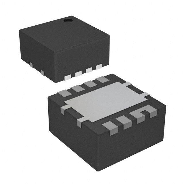
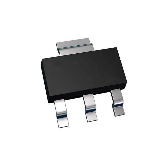
| 产品图片 |
|
| rohs | 符合RoHS无铅 / 符合限制有害物质指令(RoHS)规范要求 |
| 产品系列 | 电源管理 IC,低压差稳压器,Fairchild Semiconductor FAN2558S12X- |
| 数据手册 | |
| 产品型号 | FAN2558S12X |
| PCN封装 | |
| PCN设计/规格 | |
| 产品种类 | 低压差稳压器 |
| 供应商器件封装 | SOT-23-5 |
| 其它名称 | FAN2558S12X-ND |
| 包装 | 带卷 (TR) |
| 单位重量 | 30 mg |
| 商标 | Fairchild Semiconductor |
| 回动电压—最大值 | 400 mV |
| 安装类型 | 表面贴装 |
| 安装风格 | SMD/SMT |
| 封装 | Reel |
| 封装/外壳 | SC-74A,SOT-753 |
| 封装/箱体 | SOT-23-5 |
| 工作温度 | -40°C ~ 85°C |
| 工厂包装数量 | 3000 |
| 最大工作温度 | + 125 C |
| 最大输入电压 | 5.5 V |
| 最小工作温度 | - 40 C |
| 最小输入电压 | + 2.7 V |
| 标准包装 | 3,000 |
| 电压-跌落(典型值) | - |
| 电压-输入 | 2.7 V ~ 5.5 V |
| 电压-输出 | 1.2V |
| 电压调节准确度 | 1 % |
| 电流-输出 | 180mA |
| 电流-限制(最小值) | 260mA |
| 稳压器拓扑 | 正,固定式 |
| 稳压器数 | 1 |
| 系列 | FAN2558 |
| 线路调整率 | 0.3 % / V |
| 负载调节 | 2.5 % |
| 输出电压 | 1.2 V |
| 输出电流 | 180 mA |
| 输出端数量 | 1 Output |
| 输出类型 | Fixed |
| 零件号别名 | FAN2558S12X_NL |




- 商务部:美国ITC正式对集成电路等产品启动337调查
- 曝三星4nm工艺存在良率问题 高通将骁龙8 Gen1或转产台积电
- 太阳诱电将投资9.5亿元在常州建新厂生产MLCC 预计2023年完工
- 英特尔发布欧洲新工厂建设计划 深化IDM 2.0 战略
- 台积电先进制程称霸业界 有大客户加持明年业绩稳了
- 达到5530亿美元!SIA预计今年全球半导体销售额将创下新高
- 英特尔拟将自动驾驶子公司Mobileye上市 估值或超500亿美元
- 三星加码芯片和SET,合并消费电子和移动部门,撤换高东真等 CEO
- 三星电子宣布重大人事变动 还合并消费电子和移动部门
- 海关总署:前11个月进口集成电路产品价值2.52万亿元 增长14.8%


PDF Datasheet 数据手册内容提取
Is Now Part of To learn more about ON Semiconductor, please visit our website at www.onsemi.com Please note: As part of the Fairchild Semiconductor integration, some of the Fairchild orderable part numbers will need to change in order to meet ON Semiconductor’s system requirements. Since the ON Semiconductor product management systems do not have the ability to manage part nomenclature that utilizes an underscore (_), the underscore (_) in the Fairchild part numbers will be changed to a dash (-). This document may contain device numbers with an underscore (_). Please check the ON Semiconductor website to verify the updated device numbers. The most current and up-to-date ordering information can be found at www.onsemi.com. Please email any questions regarding the system integration to Fairchild_questions@onsemi.com. ON Semiconductor and the ON Semiconductor logo are trademarks of Semiconductor Components Industries, LLC dba ON Semiconductor or its subsidiaries in the United States and/or other countries. ON Semiconductor owns the rights to a number of patents, trademarks, copyrights, trade secrets, and other intellectual property. A listing of ON Semiconductor’s product/patent coverage may be accessed at www.onsemi.com/site/pdf/Patent-Marking.pdf. ON Semiconductor reserves the right to make changes without further notice to any products herein. ON Semiconductor makes no warranty, representation or guarantee regarding the suitability of its products for any particular purpose, nor does ON Semiconductor assume any liability arising out of the application or use of any product or circuit, and specifically disclaims any and all liability, including without limitation special, consequential or incidental damages. Buyer is responsible for its products and applications using ON Semiconductor products, including compliance with all laws, regulations and safety requirements or standards, regardless of any support or applications information provided by ON Semiconductor. “Typical” parameters which may be provided in ON Semiconductor data sheets and/or specifications can and do vary in different applications and actual performance may vary over time. All operating parameters, including “Typicals” must be validated for each customer application by customer’s technical experts. ON Semiconductor does not convey any license under its patent rights nor the rights of others. ON Semiconductor products are not designed, intended, or authorized for use as a critical component in life support systems or any FDA Class 3 medical devices or medical devices with a same or similar classification in a foreign jurisdiction or any devices intended for implantation in the human body. Should Buyer purchase or use ON Semiconductor products for any such unintended or unauthorized application, Buyer shall indemnify and hold ON Semiconductor and its officers, employees, subsidiaries, affiliates, and distributors harmless against all claims, costs, damages, and expenses, and reasonable attorney fees arising out of, directly or indirectly, any claim of personal injury or death associated with such unintended or unauthorized use, even if such claim alleges that ON Semiconductor was negligent regarding the design or manufacture of the part. ON Semiconductor is an Equal Opportunity/Affirmative Action Employer. This literature is subject to all applicable copyright laws and is not for resale in any manner.
www.fairchildsemi.com FAN2558/FAN2559 180mA Low Voltage CMOS LDO Features General Description • Fixed 1.0V, 1.2V, 1.3V, 1.5V, 1.8V, 2.5V, 3.3V, 3.5V, 3.6V, The FAN2558/9 low voltage CMOS LDOs feature fixed or 3.8V and Adjustable Output adjustable output voltage, 180mA load current, delayed • Power Good Indicator with Open Drain Output power good output (open drain) and 1% output accuracy • 180mA Output Current with excellent line and load regulation. An external bypass • 100µA Ground Current capacitor provides ultra-low noise operation. • C for Low Noise Operation bypass • Fast Enable for CDMA Applications The FAN2558/9 low voltage LDOs incorporate both thermal • High Ripple Rejection shutdown and short circuit protection. Output is stable with a • Current Limit 1µF, low ESR capacitor. The FAN2558/9 family is available • Thermal Shutdown in 5-Lead SOT-23, 6-Lead SOT-23 and 2x2mm MLP-6 • Excellent Line and Load Regulation packages. • Requires Only 1µF Output Capacitor • Stable with 0 to 300mΩ ESR FAN2558: Fixed Output LDO with Power Good output • TTL-level Compatible Enable Input • Active Output Discharge FAN2558ADJ: Adjustable Output LDO with Power Good output Applications FAN2559: Fixed Output LDO with Power Good output, • Processor Power-up sequencing Low Noise • PDAs, Cell Phones • Portable Electronic Equipment Available standard output voltages are 1.0, 1.2V, 1.3V, 1.5V, • PCMCIA Vcc and Vpp regulation/switching 1.8V, 2.5V, 3.3V, 3.5V, 3.6V, and 3.8V. Custom output volt- age options are also available. Typical Application 47KΩ 47KΩ 47KΩ R PG R PG R PG FB FB FB V IN V OUT V IN V OUT V IN V OUT SHDN C OUT SHDN R 1 C OUT SHDN C OUT CGNADP+ GCNADP+ A DJ R 2 GCNADP+C BYP C BYP ECNAP- PG ECNAP- PG ECNAP- PG FAN2558 FAN2558ADJ FAN2559 REV. 1.0.4 3/15/04
FAN2558/FAN2559 PRODUCT SPECIFICATIONS Pin Assignments TOP-VIEW V IN 1 5 VOUT V IN 1 6 VOUT V OUT 1 6 V IN NC/ADJ/BYP 2 5 GND GND 2 GND 2 5 ADJ/BYP PG 3 4 EN EN 3 4 PG EN 3 4 PG FAN2558 FAN2558ADJ/FAN2559 FAN2558/FAN2558ADJ/FAN2559 5-Lead SOT-23 PACKAGE 6-Lead SOT-23 PACKAGE 2x2mm MLP-6 PACKAGE Pin Name Pin no. FAN2558 FAN2558ADJ FAN2559 5SOT-23 2x2mm MLP-6 6SOT-23 2x2mm MLP-6 6SOT-23 2x2mm MLP-6 1 V V V V V V IN OUT IN OUT IN OUT 2 GND. NC GND. ADJ GND. BYP 3 EN PG EN PG EN PG 4 PG EN PG EN PG EN 5 V GND ADJ GND BYP GND OUT 6 V V V V V IN OUT IN OUT IN Pin Descriptions Symbol Pin Function Description V Power Supply Input IN V Regulated Voltage Output OUT GND Ground Connection PG Power Good Output, Open Drain ADJ Ratio of potential divider from V to ADJ determines output voltage out BYP Reference Noise Bypass EN Chip Enable Input. The regulator is fully enabled when TTL “H” is applied to this input. The regulator enters into shutdown mode when TTL “L” is applied to this input. 2 REV. 1.0.4 3/15/04
PRODUCT SPECIFICATIONS FAN2558/FAN2559 Absolute Maximum Ratings Parameter Min. Max. Units V to GND 6 V IN Voltage on any other pin to GND -0.3 V + 0.3 V IN Junction Temperature (T ) -55 150 °C J Storage Temperature -65 150 °C Lead Soldering Temperature, 10 seconds 300 °C Power Dissipation (P ) Internally W D Limited Electrostatic Discharge (ESD) Protection (Note1) HBM 4 kV CDM 1 Recommended Operating Conditions Parameter Min. Typ. Max. Units Supply Voltage Range, V for V < 2.0V 2.7 5.5 V IN OUT Supply Voltage Range, V for V ≥ 2.0V V + V 5.5 V IN OUT OUT DROPOUT Load Current 180 mA Enable Input Voltage V 0 V V EN IN Power Good Output Voltage Range V 0 V V PG IN Junction Temperature -40 125 °C Thermal Resistance-Junction to Ambient SOT-23 (Note 2) 235 Thermal Resistance-Junction to Case, 2mm x 2mm 75 °C/W 6-lead MLP Notes: 1. Using Mil Std. 883E, method 3015.7 (Human Body Model) and EIA/JESD22C101-A (Charge Device Model) 2. Junction to ambient thermal resistance, Θ , is a strong function of PCB material, board thickness, thickness and number of JC copper plains, number of via used, diameter of via used, available copper surface, and attached heat sink characteristics. REV. 1.0.4 3/15/04 3
FAN2558/FAN2559 PRODUCT SPECIFICATIONS Electrical Characteristics V = V min (note 5) to 5.5V, V = V , I = 100µA, T = -40°C to +85°C, unless otherwise noted. Typical values IN IN EN IN LOAD A are at 25°C. Symbol Parameter Conditions Min. Typ. Max. Units V Output Voltage Accuracy I = 100µA -2 1 2 % OUT LOAD (Note 3) V Output Voltage Range I = 100µA 1 V V OUT(ADJ) LOAD IN (Adjustable) ∆V Line Regulation V min < V < 5.5V -0.3 0.3 %/V OUT_LNR IN IN ∆V Load Regulation (Note 4) I = 0.1mA to 150mA 2.5 4 % OUT_LDR LOAD I Supply Current in Shutdown V < 0.4V 0.1 µA SD EN Mode PG = No Connection I Ground Pin Current (Note 4) I = 0mA, V = 5.5V 90 150 GND LOAD IN µA I = 150mA, V = 5.5V 110 150 LOAD IN I Current Limit V = 0V 260 350 500 mA LIM OUT T Thermal Shutdown 150 °C SD Temperature Thermal Shutdown Hysteresis 10 °C V Enable Input Low V = 5.5V, Shutdown 0.4 V ENL IN V Enable Input High V = 5.5V, Enabled 1.6 V ENH IN I Enable Input Current V ≤ 0.4V, V = 5.5V 0.01 E ENL IN µA V ≥ 1.6V, V = 5.5V 0.01 ENH IN V Low Threshold % of V PG ON 89 % PG OUT High Threshold % of V PG OFF 97 % OUT V PG Output Low Voltage I = 100µA, 0.02 0.1 V PGL PG_SINK Fault Condition I PG Leakage Current PG off, V =5.5V 0.01 µA PG PG T Enable Response Time C = 1µF 30 300 µS EN OUT C = 10nF BYPASS T Power "ON" Delay Time C = 1µF 300 500 µS ON OUT C = 10nF BYPASS V ≥ 1.6V, ENL V = 0V to V + 1V IN OUT D PG Delay time 1 5 mS PG V Dropout Voltage V > 2.7V and 400 mV DROP-OUT OUT (For Adjustable Output I = 180mA LOAD Version) V Feedback Voltage 0.59 V FB_ADJ (For Adjustable Output Version) Note: 3. Guaranteed ±1% output voltage accuracy parts are available on customer request. 4. Measured at constant junction temperature using low duty cycle pulse testing. 5. V min = 2.7V or (V + 1V), whichever is greater. IN OUT 4 REV. 1.0.4 3/15/04
PRODUCT SPECIFICATIONS FAN2558/FAN2559 DC Electrical Characteristics (Continued) V = V min (note 5) to 5.5V, V = V , I = 100µA, T = -40°C to +85°C, unless otherwise noted. Typical IN IN EN IN LOAD A values are at 25°C. Symbol Parameter Conditions Min. Typ. Max. Units PSRR Power Supply Rejection Ratio DC to 100kHz 50 dB C =1µF OUT C = 10nF BYPASS I = 0 to 150mA LOAD V ≤ 1.8V OUT e Output Noise BW: 300Hz to 50kHz 30 µV N RMS C =1µF OUT C = 10nF BYPASS I = 0 to 150mA LOAD REV. 1.0.4 3/15/04 5
FAN2558/FAN2559 PRODUCT SPECIFICATIONS Functional Description capacitor quality still must be considered if the designer is to achieve optimal circuit performance. In general, ceramic Utilizing BiCMOS technology, the FAN2525/FAN2559 capacitors offer superior ESR performance, and a smaller product family is optimized for use in compact battery pow- case size than tantalum capacitors. ered systems. These LDOs offer a unique combination of high ripple rejection, low noise, low power consumption, Input Capacitor high tolerance for a variety of output capacitors, and less An input capacitor of 2.2µF (nominal value) or greater, than 1µA “OFF” current. In the circuit, a differential current connected between the Input pin and Ground, placed in close sense amplifier controls a series-pass P-Channel MOSFET to proximity to the device, will improve transient response and achieve high ripple rejection. A separate error amplifier com- ripple rejection. Higher values will further improve ripple pares the load voltage at the output with an onboard trimmed rejection and transient response. An input capacitor is rec- low voltage bandgap reference for output regulation. ommended when the input source, either a battery or a regu- lated AC voltage, is located far from the device. Any good Thermal shutdown and current limit circuits protect the quality ceramic, tantalum, or metal film capacitor will give device under extreme conditions. When the device tempera- acceptable performance; however, in extreme cases capacitor ture reaches 150°C, the output is disabled. When the device surge current ratings may have to be considered. cools down by 10°C, it is re-enabled. The user can shut down the device using the Enable control pin at any time. The cur- Output Capacitor rent limit circuit is trimmed, which leads to consistent power on /enable delays, and provides safe short circuit current An output capacitor is required to maintain regulator loop densities even in narrow traces of the PCB. stability. Stable operation will be achieved with a wide vari- ety of capacitors with ESR values ranging from 0mΩ up to A carefully optimized control loop accommodates a wide 400mΩ. Multilayer ceramic, tantalum or aluminum electro- range of ESR values in the output bypass capacitor, allowing lytic capacitors may be used. A nominal value of at least 1µF the user to optimize space, cost, and performance require- is recommended. Note that the choice of output capacitor ments. affects load transient response, ripple rejection, and it has a slight effect on noise performance as well. An Enable pin shuts down the regulator output to conserve power, reducing supply current to less than 1µA. An internal resistor of approximately 100Ω is connected between V and GND in shutdown mode, to discharge the OUT The fixed-voltage FAN2559 has a noise bypass pin. Power output capacitor at a faster rate. Good is available as a diagnostic function to indicate that the output voltage has reduced within 5% of the nominal value. Bypass Capacitor (FAN2559 Only) In the fixed-voltage configuration, connecting a capacitor The six pin adjustable-voltage version utilizes pin 5 to con- between the bypass pin and ground can significantly reduce nect to an external voltage divider which feeds back to the output noise. Values ranging from 0pF to 47nF can be used, regulator error amplifier, thus setting the output voltage to depending on the sensitivity to output noise in the applica- the desired value. tion. Applications Information At the high-impedance Bypass pin, care must be taken in the PCB layout to minimize noise pickup, and capacitors must External Capacitors – Selection be selected to minimize current loading (leakage). Noise The FAN2558/FAN2559 gives the user the flexibility to uti- pickup from external sources can be considerable. Leakage lize a wide variety of capacitors compared to other LDOs. currents into the Bypass pin will directly affect regulator An innovative design approach offers significantly reduced accuracy and should be kept as low as possible; thus, high- sensitivity to ESR, which degrades regulator loop stability in quality ceramic and film types are recommended for their older designs. While the improvements featured in the low leakage characteristics. Cost-sensitive applications not FAN2558/FAN2559 family greatly simplify the design task, concerned with noise can omit this capacitor. 6 REV. 1.0.4 3/15/04
PRODUCT SPECIFICATIONS FAN2558/FAN2559 Control Functions The ground pin current I can be found in the charts GND provided in the Electrical Characteristics section. Enable Pin Connecting 2V or greater to the Enable pin will enable the The relationship describing the thermal behavior of the output, while 0.4V or less will disable it while reducing the package is: qduowiensc feunnt cctuiornre inst ncootn nsueemdpetdio, nth teo p liens sc athna sni m1µpAly. bIfe tchoisn -shut- PD(max) = T----J---(-m----θa---x---)---–----T----A-- JA nected permanently to the V pin. Allowing this pin to float IN will cause erratic operation. where T is the maximum allowable junction tempera- J(max) ture of the die, which is 125°C, and T is the ambient operat- A Error Flag (Power Good) ing temperature. θ is dependent on the surrounding PC JA Fault conditions such as input voltage dropout (low VIN), board layout and can be empirically obtained. While the θJC overheating, or overloading (excessive output current), will (junction-to-case) of the SOT23-5 package is specified at set an error flag. The PG pin which is an open-drain output, 130°C /W, the θJA of the minimum PWB footprint will be at will go LOW when V is less than 95% or the specified least 235°C /W. This can be improved by providing a heat OUT output voltage. When the voltage at V is greater than sink of surrounding copper ground on the PWB. Depending 95% of the specified output voltage, thOeU PTG pin is HIGH. A on the size of the copper area, the resulting θJA can range logic pull-up resistor of 47KΩ is recommended at this out- from approximately 180°C /W for one square inch to nearly put. The pin can be left disconnected if unused. 130°C /W for 4 square inches. The addition of backside cop- per with through-holes, stiffeners, and other enhancements Thermal Protection can also aid in reducing thermal resistance. The heat contrib- uted by the dissipation of other devices located nearby must The FAN2558/FAN2559 is designed to supply high peak be included in the design considerations. Once the limiting output currents for brief periods, however sustained exces- parameters in these two relationships have been determined, sive output load at high input - output voltage difference will the design can be modified to ensure that the device remains increase the device’s temperature and exceed maximum rat- within specified operating conditions. If overload conditions ings due to power dissipation. During output overload condi- are not considered, it is possible for the device to enter a tions, when the die temperature exceeds the shutdown limit thermal cycling loop, in which the circuit enters a shutdown temperature of 150°C, an onboard thermal protection will condition, cools, re-enables, and then again overheats and disable the output until the temperature drops approximately shuts down repeatedly due to an unmanaged fault condition. 10°C below the limit, at which point the output is re-enabled. During a thermal shutdown, the user may assert the power- Adjustable Version down function at the Enable pin, reducing power consump- tion to a minimum. The FAN2558ADJ includes an input pin ADJ which allows the user to select an output voltage ranging from 1V to near Thermal Characteristics V , using an external resistor divider. The voltage V pre- IN ADJ sented to the ADJ pin is fed to the onboard error amplifier The FAN2558/FAN2559 is designed to supply 180mA at the which adjusts the output voltage until V is equal to the specified output voltage with an operating die (junction) ADJ onboard bandgap reference voltage of 1.00V(typ). The equa- temperature of up to 125°C. Once the power dissipation and tion is: thermal resistance is known, the maximum junction tempera- R ture of the device can be calculated. While the power dissipa- V = 0.59V× 1+-----1- OUT R tion is calculated from known electrical parameters, the 2 actual thermal resistance depends on the thermal characteris- Since the bandgap reference voltage is trimmed, 1% initial tics of the SOT23-5 surface-mount package and the sur- accuracy can be achieved. The total value of the resistor rounding PC board copper to which it is mounted. chain should not exceed 250KOhm total to keep the error amplifier biased during no-load conditions. Programming The power dissipation is equal to the product of the input-to- output voltages very near V need to allow for the magni- output voltage differential and the output current plus the IN tude and variation of the dropout voltage V over load, sup- ground current multiplied by the input voltage, DO ply, and temperature variations. Note that the low-leakage or: FET input to the CMOS error amplifier induces no bias PD = (VIN–VOUT)×IOUT+VIN×IGND current error to the calculation. REV. 1.0.4 3/15/04 7
FAN2558/FAN2559 PRODUCT SPECIFICATIONS General PCB Layout Considerations load conditions. A large copper area in the local ground serves as heat sink (as discussed above) when high power For optimum device performance, careful circuit layout and dissipation significantly increases device temperature. Com- grounding techniques must be used. Establishing a small ponent-side copper provides significantly better thermal per- local ground, to which the GND pin, and the output and formance. Added feed through connecting the device side bypass capacitors are connected, is recommended. The input ground plane to the back plane further reduces thermal resis- capacitor should be grounded to the main ground plane. The tance. quiet local ground is then routed back to the main ground plane using feed through via. In general, the high-frequency compensation components (input, bypass, and output capaci- tors) should be located as close to the device as possible. Close proximity of the output capacitor is especially impor- tant to achieve optimum performance, especially during high 8 REV. 1.0.4 3/15/04
PRODUCT SPECIFICATIONS FAN2558/FAN2559 Block Diagram (Note 6) VIN EN Shutdown BYPASS Bandgap Precharge/Fast Enable Control Shutdown Load Current p Error Amplifier Thermal Sense Shutdown VOUT n GND Out of Regulation Detection PG n Delay Over-Current Dropout Detection GND Note: 6. Fixed output voltage version. BYPASS pin is available for FAN2559 only. REV. 1.0.4 3/15/04 9
FAN2558/FAN2559 PRODUCT SPECIFICATIONS Typical Performance Characteristics Unless otherwise specified, C = C = 1µF, R = 47kΩ, T = 25°C, EN = V IN OUT PG A IN Output Voltage vs. Temperature Output Voltage vs. Temperature ILOAD = 0mA ge (V) VIN = 5.5V e (V) ILOVADIN = = 1 58.05mVA a g Volt olta put ut V Out utp O Junction Temperature (°C) Junction Temperature (°C) Ground Current vs. Temperature Ground Current vs. Temperature A) ILOAD = 0mA VIN = 5.5V ILOAD = 180mA VIN = 5.5V µ A) Current ( µurrent ( Ground VIN = 2.7V Ground C VIN = 2.7V Junction Temperature (°C) Junction Temperature (°C) Enable Response Time vs. Temperature Power On Response Time vs. Temperature S) µy (S) µelay ( a D Del On able wer n o E P Junction Temperature (°C) Junction Temperature (°C)) 10 REV. 1.0.4 3/15/04
PRODUCT SPECIFICATIONS FAN2558/FAN2559 Typical Performance Characteristics (Continued) Unless otherwise specified, C = C = 1µF, R = 47kΩ, T = 25°C, EN = V IN OUT PG A IN Power Good Delay vs. Input Voltage Output Voltage vs. Input Voltage S) ILOAD = 100µA m Delay ( age (V) ILOAD =100µA Good ut Volt ower Outp P ILOAD =180mA Input Voltage (V) Input Voltage (V) Output Voltage vs. Load Current Output Voltage vs. Enable Voltage COUT =1µF COUT =1µF Output Voltage (V) VIN =2.7V Output Voltage (V) ILOAD =100µA Load Current (mA) Enable Voltage (V) Ripple Rejection vs. Frequency Ripple Rejection vs. Frequency VOUT ≤ 1.8V on (dB) VOUT ≤ 1.8V ICCLOOBAYUDPT ===0 11mµ0FAnF n (dB) ICCLOOBAYUDPT === 1118µ00FnmFA ecti ctio Rej eje pple ple R Ri Rip REV. 1.0.4 3/15/04 11
FAN2558/FAN2559 PRODUCT SPECIFICATIONS Typical Performance Characteristics (Continued) Unless otherwise specified, C = C = 1µF, R = 47kΩ, T = 25°C, EN = V IN OUT PG A IN Output Spectral Noise Density /rtHz)ms CCILBOOYAUPDT = == 1 110µ8nF0FmA Enable Voltage(2V/div) Enable Delay = 27.6µS VOUT =1.2V Vr Noise (n put Voltage00mV/div) ICCVLOOBINYAU DP=T 2===.0171m0VµnFAF ut(5 O Time (20µS/div) Load Transient Response Power Good Delay agev) VVOINU =T 2=.17.V8V Power Good Delay = 2mSec VVOINU =T3 =V1V VoltV/di COUT = 4.7µF e COUT =1µF Output (100m ILOAD =100mA Output Voltag(1V/div) nt e Output Curr(50mA/div) ILOAD = 0mA ower Good(2V/div) P Time (200µS/div) Time (1mS/div) Power Good in Fail Condition 25 20 VIN = 4V A) m nt ( 15 VIN = 5V e urr d C 10 VIN = 3V o o G er 5 w o P 0 0.0 0.5 1.0 1.5 2.0 Power Good Voltage (V) 12 REV. 1.0.4 3/15/04
PRODUCT SPECIFICATIONS FAN2558/FAN2559 Mechanical Dimensions 2x2mm 6-Lead MLP REV. 1.0.4 3/15/04 13
FAN2558/FAN2559 PRODUCT SPECIFICATIONS Mechanical Dimensions 6-Lead SOT-23 Package 5-Lead SOT-23 Package B B e e c c L L E H E H α α e1 e1 D D A A A1 A1 Symbol Inches Millimeters Notes Min Max Min Max A .035 .057 .90 1.45 A1 .000 .006 .00 .15 B .008 .020 .20 .50 c .003 .010 .08 .25 D .106 .122 2.70 3.10 E .059 .071 1.50 1.80 e .037 BSC .95 BSC e1 .075 BSC 1.90 BSC H .087 .126 2.20 3.20 L .004 .024 .10 .60 α 0° 10° 0° 10° Notes: 7. Package outline exclusive of mold flash & metal burr. 8. Packageoutline exclusive of solder plating. 9. EIAJ Ref Number SC_74A 14 REV. 1.0.4 3/15/04
PRODUCT SPECIFICATIONS FAN2558/FAN2559 Ordering Information T = -40°C to 85°C A Part Number Output Voltage Package Marking Package Order Code FAN2558 1.0V 58T 5-Lead SOT-23 FAN2558S10X 1.2V 58U FAN2558S12X 1.3V 58X FAN2558S13X 1.5V 58V FAN2558S15X 1.8V 58O FAN2558S18X 2.5V 58J FAN2558S25X 3.3V 58K FAN2558S33X 3.5V 58P FAN2558S35X 3.6V 58Q FAN2558S36X 3.8V 58I FAN2558S38X 1.0V 58T 2mm x 2mm 6-Lead MLP FAN2558MP10X 1.2V 58U FAN2558MP12X 1.3V 58X FAN2558MP13X 1.5V 58V FAN2558MP15X 1.8V 58O FAN2558MP18X Adjustable 58R 6-Lead SOT-23 FAN2558SX 58R 2mm x 2mm 6-Lead MLP FAN2558MPX FAN2559 1.0V 59T 6-Lead SOT-23 FAN2559S10X 1.2V 59U FAN2559S12X 1.3V 59X FAN2559S13X 1.5V 59V FAN2559S15X 1.8V 59O FAN2559S18X 1.0V 59T 2mm x 2mm 6-Lead MLP FAN2559MP10X 1.2V 59U FAN2559MP12X 1.3V 59X FAN2559MP13X 1.5V 59V FAN2559MP15X 1.8V 59O FAN2559MP18X DISCLAIMER FAIRCHILD SEMICONDUCTOR RESERVES THE RIGHT TO MAKE CHANGES WITHOUT FURTHER NOTICE TO ANY PRODUCTS HEREIN TO IMPROVE RELIABILITY, FUNCTION OR DESIGN. FAIRCHILD DOES NOT ASSUME ANY LIABILITY ARISING OUT OF THE APPLICATION OR USE OF ANY PRODUCT OR CIRCUIT DESCRIBED HEREIN; NEITHER DOES IT CONVEY ANY LICENSE UNDER ITS PATENT RIGHTS, NOR THE RIGHTS OF OTHERS. LIFE SUPPORT POLICY FAIRCHILD’S PRODUCTS ARE NOT AUTHORIZED FOR USE AS CRITICAL COMPONENTS IN LIFE SUPPORT DEVICES OR SYSTEMS WITHOUT THE EXPRESS WRITTEN APPROVAL OF THE PRESIDENT OF FAIRCHILD SEMICONDUCTOR CORPORATION. As used herein: 1. Life support devices or systems are devices or systems 2. A critical component in any component of a life support which, (a) are intended for surgical implant into the body, device or system whose failure to perform can be or (b) support or sustain life, and (c) whose failure to reasonably expected to cause the failure of the life support perform when properly used in accordance with device or system, or to affect its safety or effectiveness. instructions for use provided in the labeling, can be reasonably expected to result in a significant injury of the user. www.fairchildsemi.com REV. 1.0.4 3/15/04 2004 Fairchild Semiconductor Corporation
ON Semiconductor and are trademarks of Semiconductor Components Industries, LLC dba ON Semiconductor or its subsidiaries in the United States and/or other countries. ON Semiconductor owns the rights to a number of patents, trademarks, copyrights, trade secrets, and other intellectual property. A listing of ON Semiconductor’s product/patent coverage may be accessed at www.onsemi.com/site/pdf/Patent−Marking.pdf. ON Semiconductor reserves the right to make changes without further notice to any products herein. ON Semiconductor makes no warranty, representation or guarantee regarding the suitability of its products for any particular purpose, nor does ON Semiconductor assume any liability arising out of the application or use of any product or circuit, and specifically disclaims any and all liability, including without limitation special, consequential or incidental damages. Buyer is responsible for its products and applications using ON Semiconductor products, including compliance with all laws, regulations and safety requirements or standards, regardless of any support or applications information provided by ON Semiconductor. “Typical” parameters which may be provided in ON Semiconductor data sheets and/or specifications can and do vary in different applications and actual performance may vary over time. All operating parameters, including “Typicals” must be validated for each customer application by customer’s technical experts. ON Semiconductor does not convey any license under its patent rights nor the rights of others. ON Semiconductor products are not designed, intended, or authorized for use as a critical component in life support systems or any FDA Class 3 medical devices or medical devices with a same or similar classification in a foreign jurisdiction or any devices intended for implantation in the human body. Should Buyer purchase or use ON Semiconductor products for any such unintended or unauthorized application, Buyer shall indemnify and hold ON Semiconductor and its officers, employees, subsidiaries, affiliates, and distributors harmless against all claims, costs, damages, and expenses, and reasonable attorney fees arising out of, directly or indirectly, any claim of personal injury or death associated with such unintended or unauthorized use, even if such claim alleges that ON Semiconductor was negligent regarding the design or manufacture of the part. ON Semiconductor is an Equal Opportunity/Affirmative Action Employer. This literature is subject to all applicable copyright laws and is not for resale in any manner. PUBLICATION ORDERING INFORMATION LITERATURE FULFILLMENT: N. American Technical Support: 800−282−9855 Toll Free ON Semiconductor Website: www.onsemi.com Literature Distribution Center for ON Semiconductor USA/Canada 19521 E. 32nd Pkwy, Aurora, Colorado 80011 USA Europe, Middle East and Africa Technical Support: Order Literature: http://www.onsemi.com/orderlit Phone: 303−675−2175 or 800−344−3860 Toll Free USA/Canada Phone: 421 33 790 2910 Fax: 303−675−2176 or 800−344−3867 Toll Free USA/Canada Japan Customer Focus Center For additional information, please contact your local Email: orderlit@onsemi.com Phone: 81−3−5817−1050 Sales Representative © Semiconductor Components Industries, LLC www.onsemi.com www.onsemi.com 1
Mouser Electronics Authorized Distributor Click to View Pricing, Inventory, Delivery & Lifecycle Information: O N Semiconductor: FAN2558S36X FAN2558S38X FAN2558S33X FAN2558S25X FAN2558SX FAN2558MP13X FAN2558MP18X FAN2558MP10X FAN2558MP15X FAN2558MP12X FAN2558S12X FAN2558MPX FAN2558S10X FAN2558S18X FAN2558S13X FAN2558S15X FAN2558S35X
 Datasheet下载
