ICGOO在线商城 > EZA-DT51AAAJ
 Datasheet下载
- 型号: EZA-DT51AAAJ
- 制造商: Panasonic Corporation
- 库位|库存: xxxx|xxxx
- 要求:
| 数量阶梯 | 香港交货 | 国内含税 |
| +xxxx | $xxxx | ¥xxxx |
查看当月历史价格
查看今年历史价格
EZA-DT51AAAJ产品简介:
ICGOO电子元器件商城为您提供EZA-DT51AAAJ由Panasonic Corporation设计生产,在icgoo商城现货销售,并且可以通过原厂、代理商等渠道进行代购。 提供EZA-DT51AAAJ价格参考以及Panasonic CorporationEZA-DT51AAAJ封装/规格参数等产品信息。 你可以下载EZA-DT51AAAJ参考资料、Datasheet数据手册功能说明书, 资料中有EZA-DT51AAAJ详细功能的应用电路图电压和使用方法及教程。
| 参数 | 数值 |
| 产品目录 | |
| 描述 | RC NETWORK 470 OHM/22PF 5% SMD |
| ESD保护 | 无 |
| 产品分类 | EMI/RFI 滤波器(LC、RC 网络) |
| 品牌 | Panasonic Electronic Components |
| 数据手册 | |
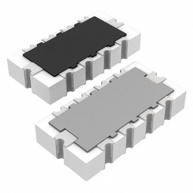
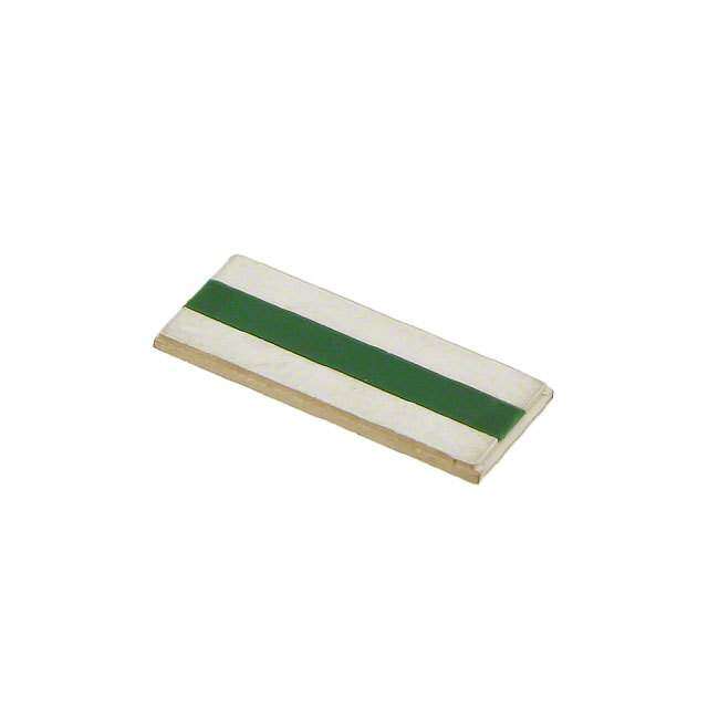
| 产品图片 |
|
| 产品型号 | EZA-DT51AAAJ |
| rohs | 含铅 / 不符合限制有害物质指令(RoHS)规范要求 |
| 产品系列 | EZADT |
| 中心/截止频率 | - |
| 产品目录绘图 |
|
| 产品目录页面 | |
| 其它名称 | PDT51CT |
| 包装 | 剪切带 (CT) |
| 大小/尺寸 | 0.126" 长 x 0.063" 宽(3.20mm x 1.60mm) |
| 封装/外壳 | 1206(3216 公制),凹面,长边端子 |
| 工作温度 | -25°C ~ 85°C |
| 应用 | 移动设备的数据线路 |
| 技术 | RC(Pi) |
| 数值 | R = 470 欧姆,C = 22pF |
| 标准包装 | 1 |
| 滤波器阶数 | 4th |
| 电流 | - |
| 电阻-通道(Ω) | 470 |
| 类型 | 低通 |
| 衰减值 | - |
| 通道数 | 4 |
| 高度 | 0.033"(0.85mm) |


- 商务部:美国ITC正式对集成电路等产品启动337调查
- 曝三星4nm工艺存在良率问题 高通将骁龙8 Gen1或转产台积电
- 太阳诱电将投资9.5亿元在常州建新厂生产MLCC 预计2023年完工
- 英特尔发布欧洲新工厂建设计划 深化IDM 2.0 战略
- 台积电先进制程称霸业界 有大客户加持明年业绩稳了
- 达到5530亿美元!SIA预计今年全球半导体销售额将创下新高
- 英特尔拟将自动驾驶子公司Mobileye上市 估值或超500亿美元
- 三星加码芯片和SET,合并消费电子和移动部门,撤换高东真等 CEO
- 三星电子宣布重大人事变动 还合并消费电子和移动部门
- 海关总署:前11个月进口集成电路产品价值2.52万亿元 增长14.8%


PDF Datasheet 数据手册内容提取
Chip RC Networks Chip RC Networks Type: EZACT Type: EZASTB/SSB EZADT EZAST/SS EZANT GND GND GND GND ■ Features Smallest SMD R/C networks ● 4 popular noise reduction circuits made EZACT : 2.0 mm (cid:1) 1.2 mm (cid:1) 0.6 mm, 0.5 mm pitch (Flat terminal type) EZADT : 3.2 mm (cid:1) 1.6 mm (cid:1) 0.65 mm, 0.635 mm pitch (Concave terminal type) EZAST/SS : 4.0 mm (cid:1) 2.1 mm (cid:1) 0.65 mm, 0.8 mm pitch (Concave terminal type) EZASTB/SSB : 4.0 mm (cid:1) 2.1 mm (cid:1) 0.65 mm, 0.65 mm pitch (Convex terminal type) EZANT : 6.4 mm (cid:1) 3.1 mm (cid:1) 0.80 mm, 1.27 mm pitch (Concave terminal type) ● Takes up less space than discrete chip resistor & chip capacitor EZACT:25 % of 0402 inches (1.0 mm (cid:1) 0.5 mm) chips placing area EZADT:50 % of 0402 inches (1.0 mm (cid:1) 0.5 mm) chips placing area EZAST/SS, EZASTB/SSB:70 % of 0402 inches (1.0 mm (cid:1) 0.5 mm) chips placing area EZANT:55 % of 0805 inches (2.0 mm (cid:1) 1.2 mm) chips placing area <Effect of high density placing, PWB space saving> RC Low pass fi lter AC Terminator I/O I/O I/O I/O ChipRCNetwork (EZACT,EZADT,EZAST/SS,EZANT) I/O I/O I/O I/O ChipRCNetwork (EZACT,EZADT,EZAST/SS,EZANT) DiscreteChips I/O I/O DiscreteChips I/O I/O ChipRCNetwork (EZASTB/SSB) ChipRCNetwork (EZASTB/SSB) ■ Recommended Applications ● Digital equipment such as PCs, printers, HDD, PCMCIA cards, PDAs, and word processors ● Communication equipment, digital cordless phones, automobile phones, GSM, PHS, DECT ● Digital audio and video equipment ● Electronic musical instruments, and other digital devices Design and specifi cations are each subject to change without notice. Ask factory for the current technical specifi cations before purchase and/or use. Should a safety concern arise regarding this product, please be sure to contact us immediately. 00 Sep. 2010 – 261 –
Chip RC Networks ■ Explanation of Part Numbers ● EZACT • EZADT • EZAST • EZANT (R/C Standard Combination) 1 2 3 4 5 6 7 8 9 10 11 12 E Z A S T 3 3 A A A J CommonCode Dimensionand R/CStandardCombination Design Resistance SuffixforSpecial CircuitConfiguration Configuration Tolerance Requirement TShuipcpkrFeislmsioNnoaisned CT 2(cid:1).01.m2mmm RCeosnifsigtaunracteioVna✽lu1e CCaopnfaigcuitarantcioenV✽a2lue AAA Standard J ±5% FCioltemrpinognents DT 3(cid:1).21.m6mmm ChipRC 01 1202(cid:2)(cid:2) 01 1202ppFF ST 4(cid:1).02.m1mmm Networks 23 14070(cid:2)(cid:2) 23 14070ppFF NT 6(cid:1).43.m1mmm 45 242700(cid:2)(cid:2) 45 242700ppFF 6 1k(cid:2) 6 1000pF ✽122(cid:2)to1k(cid:2) availableforEZADT,EZAST,andEZANT ✽210pFand22pFavailableforEZACT.22pFto100pFavailableforEZAST,EZADT.220pFto1000pFavailableforEZANT. ● EZACT • EZADT • EZASS • EZANT (R/C Except the standard Combination) 1 2 3 4 5 6 7 8 9 10 11 12 E Z A S S 7 0 1 Y A J CommonCode Dimensionand DesignNumber Resistance SuffixforSpecial CircuitConfiguration Tolerance Requirement TShuipcpkrFeislmsioNnoaisned CT 2(cid:1).01.m2mmm CT RCIneaaspbiasotcavitneac-nmeceeVnaVtliuaoelnuee:d1:0r1a0(cid:2)ngpteoF,1tiot0i03s3kp(cid:2)poFssibleto J ±5% Filtering 3.2mm chooseoptionalR/C. Components DT (cid:1)1.6mm ChipRC ResistanceValue:10(cid:2)to100k(cid:2) SS 4(cid:1).02.m1mmm Networks DT CIcnhaaopboasoceviteao-npmctieeonnVtaiaollnuRee/dC:.r1a0ngpeF,tioti1s0p0opssFibleto 6.4mm ResistanceValue:10(cid:2)to100k(cid:2) NT (cid:1)3.1mm SS CInaapbaocvitea-nmceenVtiaolnueed:r1a0ngpeF,tioti1s8p0opssFibleto chooseoptionalR/C. ResistanceValue:10(cid:2)to100k(cid:2) CapacitanceValue:220pFto1000pF NT Inabove-mentionedrange,itispossibleto chooseoptionalR/C. ● EZASTB (R/C Standard Combination) 1 2 3 4 5 6 7 8 9 10 11 12 E Z A S T B 3 3 A A J CommonCode Dimensionand R/CStandardCombination Design Resistance SuffixforSpecial CircuitConfiguration Configuration Tolerance Requirement ThickFilmNoise Convex ResistanceValue CapacitanceValue AA Standard J ±5% Suppressionand 4.0mm terminaltype Configuration Configuration STB Filtering (cid:1)2.1mm ChipRC 1 22(cid:2) 1 22pF Components Networks 2 47(cid:2) 2 47pF 3 100(cid:2) 3 100pF 4 220(cid:2) 5 470(cid:2) 6 1k(cid:2) ● EZASSB (R/C Except the standard Comb i nat ion) 1 2 3 4 5 6 7 8 9 10 11 12 E Z A S S B 7 0 1 A J CommonCode Dimensionand DesignNumber Resistance SuffixforSpecial CircuitConfiguration Tolerance Requirement ThickFilmNoise Convex ResistanceValue:10(cid:2)to100k(cid:2) J ±5% Suppressionand 4.0mm terminaltype CapacitanceValue:10pFto180pF SSB Filtering (cid:1)2.1mm ChipRC Inabove-mentionedrange,itispossibleto Components Networks chooseoptionalR/C. Design and specifi cations are each subject to change without notice. Ask factory for the current technical specifi cations before purchase and/or use. Should a safety concern arise regarding this product, please be sure to contact us immediately. 00 Sep. 2010 – 262 –
Chip RC Networks ■ Construction EZACT EZADT EZAST/SS Marking Aluminasubstrate Marking Aluminasubstrate Marking Protectivecoating Aluminasubstrate GND GND Electrode Electrode (Outer) 33 (Outer) GND GND GND Electrode Electrode Electrode Electrode (Outer) Protectivecoating Electrode (Outer) Protectivecoating Electrode (Outer) (Outer) (Outer) (Outer) EZANT EZASTB/SSB Marking Aluminasubstrate Aluminasubstrate Marking GND GND Electrode Electrode (Outer) GND (Outer) 33 Electrode GND (Outer) Electrode (Outer) Protectivecoating Electrode Protectivecoating Electrode (Outer) (Outer) ■ Circuit Config uration EZACT EZADT • EZAST/SS • EZANT EZASTB/SSB 10 9 8 7 10 9 8 7 12 11 10 9 8 7 R1 R2 R3 R4 R1 R2 R3 R4 R1 R2 R3 R4 GND 1 6 GND GND 1 6 GND C1 C2 C3 C4 C1 C2 C3 C4 C1 C2 C3 C4 2 3 4 5 2 3 4 5 1 2 3 4 5 6 R1=R2=R3=R4 R1=R2=R3=R4 GND R1=R2=R3=R4 GND C1=C2=C3=C4 C1=C2=C3=C4 C1=C2=C3=C4 Design and specifi cations are each subject to change without notice. Ask factory for the current technical specifi cations before purchase and/or use. Should a safety concern arise regarding this product, please be sure to contact us immediately. 00 Sep. 2010 – 263 –
Chip RC Networks ■ Dimensions in mm(not to scale) EZACT EZADT 0.33±0.10 10 9 8 7 10 9 8 7 1 6 ±1.250.10 ±0.400.15 1 6±0.20.1 ±1.600.15 2 3 4 5 (0.635) 2 3 4 5 (0.5) 3.20±0.15 0.65+–00..2100 2.0±0.1 0.55±0.10 0.20±0.15 0.30±0.15 0.35±0.15 0.35±0.10 ±0.400.15 ±0.250.15 ±0.450.15 ±0.400.15 Size : 0805 inches Size : 1206 inches ( ) Reference Mass (Weight) [1000 pcs.] :4 g ( ) Reference Mass (Weight) [1000 pcs.] :11 g EZAST/SS EZANT 0.5±0.2 10 9 8 7 10 9 8 7 ±0.50.2 1 33 6±0.250.20 ±2.10.2 ±0.80.2 1 6±0.250.20 ±3.10.2 2 3 4 5 2 3 4 5 (1.27) 0.65±0.20 (0.8) 4.0±0.2 0.65+–00..2100 6.4±0.2 0.80+–00..2100 0.4±0.2 0.45±0.20 0.5±0.2 0.75±0.20 ±0.50.2 ±0.40.2 ±0.90.2 ±0.550.20 Size : 1608 inches Size : 2512 inches ( ) Reference Mass (Weight) [1000 pcs.] :17 g ( ) Reference Mass (Weight) [1000 pcs.] :55 g EZASTB/SSB 0.58±0.20.4±0.2 0.25±0.15 12 11 10 9 8 7 2 33 ±30. ±0.2 0. 2.2 1 2 3 4 5 6 (0.65) 4.0±0.2 0.65+–00..2100 0.275+–00..210000 0.2+–00..21 0 2 0. ± 5 3 0. Size : 1608 inches ( ) Reference Mass (Weight) [1000 pcs.] :18 g Design and specifi cations are each subject to change without notice. Ask factory for the current technical specifi cations before purchase and/or use. Should a safety concern arise regarding this product, please be sure to contact us immediately. 00 Sep. 2010 – 264 –
Chip RC Networks ■ Ratings Item Specific ation 10 (cid:2) to 100 k(cid:2) Resistance Values EZAC Standard : 10 (cid:2), 22 (cid:2), 47 (cid:2), 100 (cid:2), 220 (cid:2), 470 (cid:2), 1 k(cid:2) EZAD/S/N Standard : 22 (cid:2), 47 (cid:2), 100 (cid:2), 220 (cid:2), 470 (cid:2), 1 k(cid:2) or st Resistance Tolerance ±5 % si Temperature Coeffic ient of Resistance (T.C.R.) ±200 (cid:1) 10–6/°C e R EZAC : 0.031 W(<70 °C(1)) Rated Power EZAD/S/N : 0.063 W(<70 °C(1)) Limiting Element Voltage 25 V(2) EZAC : 10 pF to 33 pF Standard : 10 pF, 22 pF EZAD : 10 pF to 100 pF Capacitance Values EZAS : 10 pF to 180 pF (25 °C, 1 kHz(3), 1 Vrms) Standard : 22 pF, 47 pF, 100 pF or EZAN : 220 pF to 1000 pF cit Standard : 220 pF, 470 pF, 1000 pF a Capacitance Tolerance +30 %/–20 % p a Capacitance Temperature Characteristics E Characteristic: +20 %/–55 %(–25 to +85 °C) C Dissipation Factor Less than 3 %(25, 1 kHz(3), 1 Vrms) EZAC, EZAD : 12 V Rated Voltage EZAS : 25 V EZAN : 50 V Category Temperature Range –25 °C to +85 °C (1) For resistors operated in ambient temperature above 70 °C, rated power shall be derated. (“Power Derating Curve” is shown below) (2) Rated Voltage for resistor shall be determined from (cid:3)Rated Power(cid:1)Resistance Value, or Limiting Element Voltage whichever less. (3) In measuring at 1 MHz, Capacitance and Dissipation Factor are different. 70°C 100 Power Derating Curve %) ( 80 For resistors operated in ambient temperatures above ad 70 °C, power rating shall be derated in accordance Lo 60 d with the fi gure on the right. ate 40 R 20 85°C 0 30 20 10 0 10 20 30 40 50 60 70 80 90 AmbientTemperature(°C) ■ Attenuation Characteristics ●EZACT ●EZADT 10 Attenuation(dB)––––123400000 100(cid:2)1/2020p(cid:2)F/10pF Attenuation(dB)123400000 100(cid:2)/1100010(cid:2)0p0/F47(cid:2)p/F22pF –50 50 1M 10M 100M 1G 3G 1M 10M 100M 1G 3G Frequency(Hz) Frequency(Hz) ●EZST • EZASTB ●EZANT 0 0 B) B)10 enuation(d 123000 100(cid:2)/110000(cid:2)1p/04F70p(cid:2)F/22pF enuation(d23450000 1k(cid:2)/10100k(cid:2)pF/330pF Att 40 Att60 70 50 80 1M 10M 100M 1G 3G 1M 10M 100M 1G Frequency(Hz) Frequency(Hz) MeasurementCircuit EZACT EZADT 50(cid:2) EZAST EZASTB EZANT ~ 50(cid:2) (cid:1) Design and specifi cations are each subject to change without notice. Ask factory for the current technical specifi cations before purchase and/or use. Should a safety concern arise regarding this product, please be sure to contact us immediately. 00 Sep. 2010 – 265 –
Chip RC Networks ■ Packaging Methods (Taping) ● Standard Quantity Type Kind of Taping Pitch (P) Quantity 1 EZACT Punched Carrier Taping 5000 pcs./reel EZADT EZAST/SS 4 mm EZASTB/SSB Embossed Carrier Taping 4000 pcs./reel EZANT ● Carrier Tape (Unit : mm) P1 P2 P0 φD0 E F W B T T A φD1(OnlyEmboss) Type A B W F E P P P φD T φD 1 2 0 0 1 EZACT 1.55±0.15 2.30±0.20 8.00±0.20 3.50±0.05 1.75±0.10 0.85±0.05 — EZADT 2.00±0.20 3.60±0.20 EZAST/SS 4.00±0.10 2.00±0.05 4.00±0.10 1.50+0.10 2.50±0.20 4.40±0.20 −0 1.15±0.20 EZASTB/SSB 12.00±0.30 5.50±0.20 1.75±0.20 1.50+0.10 −0 EZANT 3.50±0.20 6.80±0.20 1.30±0.20 ● Taping Reel (Unit : mm) Type φA φN φC W W 1 2 EZACT 9.0+1.0 11.4±1.0 EZADT –0 EZAST/SS 180.0+0 60+1.0 13.0±0.2 –1.5 –0 EZASTB/SSB 13.0+1.0 15.4±1.0 –0 φC EZANT N φ W1 φA W2 Design and specifi cations are each subject to change without notice. Ask factory for the current technical specifi cations before purchase and/or use. Should a safety concern arise regarding this product, please be sure to contact us immediately. 00 Sep. 2010 – 266 –
Chip RC Networks ■ Recommended Land Pattern Design ●EZACT bg P Landpattern a b c d d ae Dimensions 0.75 0.25 1.70 0.35 (mm) c e h g P h Dimensions 1.85 2.60 0.25 0.50 (mm) ●EZADT P b Landpattern a b c d Dimensions 0.9 to 1.1 0.2 to 0.3 2.6 to 2.8 0.3 to 0.4 (mm) d af f g P Dimensions 2.0 to 2.6 3.6 to 4.2 0.635 c (mm) g ●EZAST/SS Solderresistant f2 c Landpattern a b c d Dimensions d 1.2 to 1.4 0.4 3.1 to 3.3 0.4 to 0.5 (mm) f1 a e GND e f1 f2 P Dimensions 0.8 2.9 to 3.3 4.8 to 5.2 0.8 (mm) b P ●EZASTB/SSB f2 Landpattern a b c d Dimensions 1.4 to 1.6 0.35 0.45 0.3 (mm) 1a f GND f1 f2 P Dimensions 2.7 to 3.5 3.8 0.65 (mm) c d b P ●EZANT b P Landpattern a b c d Dimensions 2.3 to 2.5 0.4 to 0.6 5.6 to 5.8 0.4 to 0.8 (mm) d af f g P Dimensions 4.3 to 4.7 7.6 to 8.0 1.27 c (mm) g •Design to make GND pattern as large as possible, because high frequency noise is removed from GND terminals of chip RC network. Design and specifi cations are each subject to change without notice. Ask factory for the current technical specifi cations before purchase and/or use. Should a safety concern arise regarding this product, please be sure to contact us immediately. 00 Sep. 2010 – 267 –
Chip RC Networks ■ Recommended Soldering Conditions Recommendations and precautions are described below. ●Recommended soldering conditions for reflo w ·Refl ow soldering shall be performed a maximum of For soldering (Example : Sn/Pb) two times. Temperature Time ·Please contact us for additional information when Preheating 140 °C to 160 °C 60 s to120 s used in conditions other than those specifie d. ·Please measure the temperature of the terminals and Main heating Above 200 °C 30 s to 40 s study every kind of solder and printed circuit board Peak 235 ± 5 °C max. 10 s for solderability bef ore actual use. For lead-free soldering (Example : Sn/Ag/Cu) Peak Temperature Time Preheating 150 °C to 180 °C 60 s to 120 s ure Preheating at Main heating Above 230 °C 30 s to 40 s er mp Heating Peak max. 260 °C max. 10 s e T This product has circuits on both sides. Therefore, do not use adhesives because they may impair the products characteristics. Time ● Flow Soldering We do not recommend flo w soldering to the produ ct, because solder bridging may occur due to the narrow pitch of the terminals and the characteristics of the product may be badly affected when using adhesive to affi x it to a circuit board. Safety Precautions The following are precautions for individual products. Please also refer to the common precautions shown on page 4 of this catalog. 1. Take measures against mechanical stress during and after mounting of Chip RC Networks (hereafter called the RC networks) so as not to damage their electrodes and protective coatings. Be careful not to misplace the RC networks on the land patterns. Otherwise, solder bridging may occur. 2. Do not use halogen-based or other high-activity fl ux. Otherwise, the residue may impair the RC networks' performance and/or reliability. 3. Perform suffic ient preheating so that the difference of the solder temperature and the RC networks chip surface temperature becomes 100 °C or less. Maintain the temperature difference within 100 °C during rapid cooling by immersion into solvent after soldering. 4. When soldering with a soldering iron, never touch the RC networks' bodies with the tip of the soldering iron. When using a soldering iron with a high temperature tip, fin ish soldering as quickly as possible (within three seconds at 350 °C max.). 5. As the amount of applied solder becomes larger, the mechanical stress applied to the RC networks increases, causing problems such as cracks and faulty characteristics. Avoid applying an excessive amounts of solder. 6. Do not apply shock to the RC networks or pinch them with a hard tool (e.g. pliers and tweezers). Otherwise, the RC networks' protective coatings and bodies may be chipped, affecting their performance. 7. Avoid excessive bending of printed circuit boards in order to protect the RC networks from abnormal stress. 8. The static capacitance may decrease by a few percent from the time of shipment due to the characteristics peculiar to dielectric materials having a high dielectric constant. Design and specifi cations are each subject to change without notice. Ask factory for the current technical specifi cations before purchase and/or use. Should a safety concern arise regarding this product, please be sure to contact us immediately. 00 Sep. 2010 – 268 –
Safety Precautions (Common precautions for Fixed Resistors, Noise Suppression Device, ESD Suppressor, fuses, and MR Sensors) (cid:127) When using our products, no matter what sort of equipment they might be used for, be sure to make a written agreement on the specific ations with us in advance. The design and specifi cations in this catalog are subject to change without prior notice. (cid:127) Do not use the products beyond the specific ations described in this catalog. (cid:127) This catalog explains the quality and performance of the products as individual components. Before use, check and evaluate their operations when installed in your products. (cid:127) Install the following systems for a failsafe design to ensure safety if these products are to be used in equip ment where a defect in these products may cause the loss of human life or other signific ant dam age, such as damage to vehicles (automobile, train, vessel), traffic lights, medical equipment, aerospace equipment, electric heating appliances, combustion/gas equipment, rotating equipment, and disaster/crime prevention equipment. ✽Systems equipped with a protection circuit and a protection device ✽Systems equipped with a redundant circuit or other system to prevent an unsafe status in the event of a sing le fault (1) Precautions for use (cid:127) These products are designed and manufactured for general and standard use in general elect roni c equipment (e.g. AV equipment, home electric appliances, offic e equipment, information and communication equipment) (cid:127) These products are not intended for use in the following special conditions. Before using the products, carefully check the effects on their quality and performance, and determine whether or not they can be used. 1. In liquid, such as water, oil, chemicals, or organic solvent 2. In direct sunlight, outdoors, or in dust 3. In salty air or air with a high concentration of corrosive gas, such as Cl, H S, NH , SO , or NO 2 2 3 2 2 4. Electric Static Discharge (ESD) Environment (except ESD Suppressors) These components are sensitive to static electricity and can be damaged under static shock (ESD). Please take measures to avoid any of these environments. Smaller components are more sensitive to ESD environment. 5. Electromagnetic Environment Avoid any environment where strong electromagnetic waves exist. 6. In an environment where these products cause dew condensation 7. Sealing or coating of these products or a printed circuit board on which these products are mounted, with resin or other materials (cid:127) These products generate Joule heat when energized. Carefully position these products so that their heat will not affect the other components (except Thermal Cutoffs). (cid:127) Carefully position these products so that their temperatures will not exceed the category temperature range due to the effects of neighboring heat-generating components. Do not mount or place heat-generating components or infl ammables, such as vinyl-coated wires, near these products (except Thermal Cutoffs). (cid:127) Note that non-cleaning solder, halogen-based highly active fl ux, or water-soluble fl ux may deteriorate the performance or reliability of the products. (cid:127) Carefully select a fl ux cleaning agent for use after soldering. An unsuitable agent may deteriorate the performance or reliability. In particular, when using water or a water-soluble cleaning agent, be careful not to leave water residues. Otherwise, the insulation performance may be deteriorated. (2) Precautions for storage The performance of these products, including the solderability, is guaranteed for a year from the date of arr iva l at your company, provided that they remain packed as they were when delivered and stored at a tem pera ture of 5 °C to 35 °C and a relative humidity of 45 % to 85 %. The performance of EMI Filters is guaranteed for 6 months or a year after our delivery, provided that they are stored at a temperature of -5 °C to +40 °C and a relative humidity of 40 % to 60 %. Check the guarantee period in the specifi cations. The performance of Thermal Cut offs is guaranteed for a year after our delivery, provided that they are stored at a temperature of -10 °C to +40 °C and a relative humidity of 30 % to 75 %. Even within the above guarantee periods, do not store these products in the following conditions. Otherwise, their electrical performance and/or solderability may be deteriorated, and the packaging materials (e.g. taping materials) may be deformed or deteriorated, resulting in mounting failures. 1. In salty air or in air with a high concentration of corrosive gas, such as Cl, H S, NH , SO , or NO 2 2 3 2 2 2. In direct sunlight <Package markings> Package markings include the product number, quantity, and country of origin. In principle, the country of origin should be indicated in English. 00 Sep. 2010 – 4 –