 Datasheet下载
- 型号: EXC-24CE900U
- 制造商: Panasonic Corporation
- 库位|库存: xxxx|xxxx
- 要求:
| 数量阶梯 | 香港交货 | 国内含税 |
| +xxxx | $xxxx | ¥xxxx |
查看当月历史价格
查看今年历史价格
EXC-24CE900U产品简介:
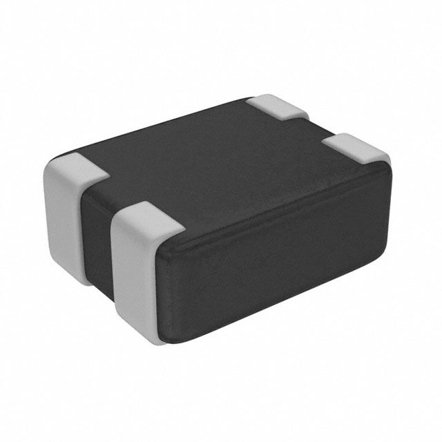
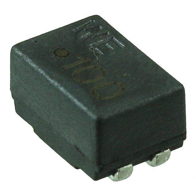
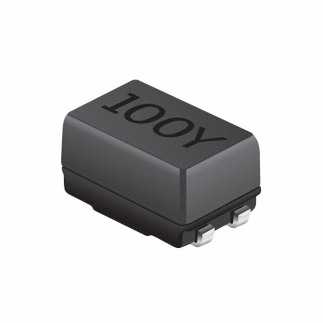
ICGOO电子元器件商城为您提供EXC-24CE900U由Panasonic Corporation设计生产,在icgoo商城现货销售,并且可以通过原厂、代理商等渠道进行代购。 EXC-24CE900U价格参考¥1.79-¥1.85。Panasonic CorporationEXC-24CE900U封装/规格:共模扼流圈, 2 线 共模扼流圈 表面贴装 90 Ohms @ 100MHz 160mA DCR 1.75 欧姆。您可以下载EXC-24CE900U参考资料、Datasheet数据手册功能说明书,资料中有EXC-24CE900U 详细功能的应用电路图电压和使用方法及教程。
Panasonic Electronic Components 的共模扼流圈型号 EXC-24CE900U 是一种用于抑制电磁干扰(EMI)的电子元件。其主要应用场景包括:

1. 通信设备:适用于网络交换机、路由器、调制解调器等设备,用于减少信号传输中的共模噪声,确保数据传输的稳定性和可靠性。

2. 消费类电子产品:可用于电视、音响系统、游戏机等设备中,防止外部电磁干扰对音频和视频信号的影响,提升用户体验。

3. 工业自动化设备:在工业控制设备、可编程逻辑控制器(PLC)以及传感器接口中使用,降低电磁干扰对控制系统的影响,保证设备的正常运行。

4. 电源系统:应用于开关电源(SMPS)、不间断电源(UPS)等场景中,抑制电源线上的共模噪声,提高电源系统的效率和稳定性。

5. 汽车电子:在车载信息娱乐系统、导航系统以及通信模块中,帮助减少车内电子设备之间的相互干扰,确保驾驶安全和舒适性。

EXC-24CE900U 的高共模阻抗特性使其能够在高频段有效抑制噪声,同时保持较低的差模插入损耗,从而不影响正常信号传输。该器件通常安装在信号线或电源线上,广泛用于需要高可靠性和低噪声环境的电子系统中。
| 参数 | 数值 |
| 产品目录 | |
| DC电阻(DCR) | 1.75 欧姆最大 |
| 描述 | NOISE FILTER COM MODE 90 OHMEMI滤波珠子、芯片与阵列 COM MODE 90Ohms NOISE FILTER |
| 产品分类 | |
| 品牌 | Panasonic Electronic Components |
| 产品手册 | |
| 产品图片 |
|
| rohs | 符合RoHS无铅 / 符合限制有害物质指令(RoHS)规范要求 |
| 产品系列 | EMI滤波珠子、芯片与阵列,Panasonic EXC-24CE900UEXC24CE |
| mouser_ship_limit | 该产品可能需要其他文件才能进口到中国。 |
| 数据手册 | |
| 产品型号 | EXC-24CE900U |
| 产品 | Common Mode Filter Arrays |
| 产品目录绘图 |
|
| 产品目录页面 | |
| 产品种类 | EMI滤波珠子、芯片与阵列 |
| 其它名称 | P12972CT |
| 包装 | 剪切带 (CT) |
| 商标 | Panasonic |
| 外壳宽度 | 1 mm |
| 外壳长度 | 1.25 mm |
| 外壳高度 | 0.5 mm |
| 大小/尺寸 | 0.049" 长 x 0.039" 宽(1.25mm x 1.00mm) |
| 安装类型 | 表面贴装 |
| 容差 | 25 % |
| 封装 | Reel |
| 封装/外壳 | 0504(1210 公制),4 引线 |
| 尺寸 | 1 mm W x 1.25 mm L x 0.5 mm H |
| 工作温度 | -40°C ~ 85°C |
| 工厂包装数量 | 5000 |
| 最大直流电流 | 160 mA |
| 最大直流电阻 | 1.75 Ohms |
| 标准包装 | 1 |
| 滤波器类型 | 数据,信号线 |
| 电压额定值 | 5 VDC |
| 电感 | - |
| 电流 | 160mA |
| 端接类型 | SMD/SMT |
| 线路数 | 2 |
| 阻抗 | 90 欧姆 |
| 高度(最大值) | 0.024"(0.60mm) |


- 商务部:美国ITC正式对集成电路等产品启动337调查
- 曝三星4nm工艺存在良率问题 高通将骁龙8 Gen1或转产台积电
- 太阳诱电将投资9.5亿元在常州建新厂生产MLCC 预计2023年完工
- 英特尔发布欧洲新工厂建设计划 深化IDM 2.0 战略
- 台积电先进制程称霸业界 有大客户加持明年业绩稳了
- 达到5530亿美元!SIA预计今年全球半导体销售额将创下新高
- 英特尔拟将自动驾驶子公司Mobileye上市 估值或超500亿美元
- 三星加码芯片和SET,合并消费电子和移动部门,撤换高东真等 CEO
- 三星电子宣布重大人事变动 还合并消费电子和移动部门
- 海关总署:前11个月进口集成电路产品价值2.52万亿元 增长14.8%


PDF Datasheet 数据手册内容提取
2020 EMC Components ESD Components Products Catalogg 2019.12
(cid:42)(cid:88)(cid:76)(cid:71)(cid:72)(cid:79)(cid:76)(cid:81)(cid:72)(cid:86)(cid:3)(cid:68)(cid:81)(cid:71)(cid:3)(cid:83)(cid:85)(cid:72)(cid:70)(cid:68)(cid:88)(cid:87)(cid:76)(cid:82)(cid:81)(cid:86)(cid:3)(cid:85)(cid:72)(cid:74)(cid:68)(cid:85)(cid:71)(cid:76)(cid:81)(cid:74)(cid:3)(cid:87)(cid:75)(cid:72) (cid:87)(cid:72)(cid:70)(cid:75)(cid:81)(cid:76)(cid:70)(cid:68)(cid:79)(cid:3)(cid:76)(cid:81)(cid:73)(cid:82)(cid:85)(cid:80)(cid:68)(cid:87)(cid:76)(cid:82)(cid:81)(cid:3)(cid:68)(cid:81)(cid:71)(cid:3)(cid:88)(cid:86)(cid:72)(cid:3)(cid:82)(cid:73)(cid:3)(cid:82)(cid:88)(cid:85)(cid:3)(cid:83)(cid:85)(cid:82)(cid:71)(cid:88)(cid:70)(cid:87)(cid:86) (cid:71)(cid:72)(cid:86)(cid:70)(cid:85)(cid:76)(cid:69)(cid:72)(cid:71)(cid:3)(cid:76)(cid:81)(cid:3)(cid:87)(cid:75)(cid:76)(cid:86)(cid:3)(cid:82)(cid:81)(cid:79)(cid:76)(cid:81)(cid:72)(cid:3)(cid:70)(cid:68)(cid:87)(cid:68)(cid:79)(cid:82)(cid:74)(cid:17) (cid:1657)(cid:3)(cid:44)(cid:73)(cid:3)(cid:92)(cid:82)(cid:88)(cid:3)(cid:90)(cid:68)(cid:81)(cid:87)(cid:3)(cid:87)(cid:82)(cid:3)(cid:88)(cid:86)(cid:72)(cid:3)(cid:82)(cid:88)(cid:85)(cid:3)(cid:83)(cid:85)(cid:82)(cid:71)(cid:88)(cid:70)(cid:87)(cid:86)(cid:3)(cid:71)(cid:72)(cid:86)(cid:70)(cid:85)(cid:76)(cid:69)(cid:72)(cid:71)(cid:3)(cid:76)(cid:81)(cid:3)(cid:87)(cid:75)(cid:76)(cid:86)(cid:3)(cid:82)(cid:81)(cid:79)(cid:76)(cid:81)(cid:72)(cid:3)(cid:70)(cid:68)(cid:87)(cid:68)(cid:79)(cid:82)(cid:74)(cid:3)(cid:73)(cid:82)(cid:85)(cid:3)(cid:68)(cid:83)(cid:83)(cid:79)(cid:76)(cid:70)(cid:68)(cid:87)(cid:76)(cid:82)(cid:81)(cid:86)(cid:3)(cid:85)(cid:72)(cid:84)(cid:88)(cid:76)(cid:85)(cid:76)(cid:81)(cid:74)(cid:3) (cid:3)(cid:86)(cid:83)(cid:72)(cid:70)(cid:76)(cid:68)(cid:79)(cid:3)(cid:84)(cid:88)(cid:68)(cid:79)(cid:76)(cid:87)(cid:76)(cid:72)(cid:86)(cid:3)(cid:82)(cid:85)(cid:3)(cid:85)(cid:72)(cid:79)(cid:76)(cid:68)(cid:69)(cid:76)(cid:79)(cid:76)(cid:87)(cid:92)(cid:15)(cid:3)(cid:82)(cid:85)(cid:3)(cid:73)(cid:82)(cid:85)(cid:3)(cid:68)(cid:83)(cid:83)(cid:79)(cid:76)(cid:70)(cid:68)(cid:87)(cid:76)(cid:82)(cid:81)(cid:86)(cid:3)(cid:90)(cid:75)(cid:72)(cid:85)(cid:72)(cid:3)(cid:87)(cid:75)(cid:72)(cid:3)(cid:73)(cid:68)(cid:76)(cid:79)(cid:88)(cid:85)(cid:72)(cid:3)(cid:82)(cid:85)(cid:3)(cid:80)(cid:68)(cid:79)(cid:73)(cid:88)(cid:81)(cid:70)(cid:87)(cid:76)(cid:82)(cid:81)(cid:3)(cid:82)(cid:73)(cid:3)(cid:87)(cid:75)(cid:72)(cid:3) (cid:3)(cid:83)(cid:85)(cid:82)(cid:71)(cid:88)(cid:70)(cid:87)(cid:86)(cid:3)(cid:80)(cid:68)(cid:92)(cid:3)(cid:71)(cid:76)(cid:85)(cid:72)(cid:70)(cid:87)(cid:79)(cid:92)(cid:3)(cid:77)(cid:72)(cid:82)(cid:83)(cid:68)(cid:85)(cid:71)(cid:76)(cid:93)(cid:72)(cid:3)(cid:75)(cid:88)(cid:80)(cid:68)(cid:81)(cid:3)(cid:79)(cid:76)(cid:73)(cid:72)(cid:3)(cid:82)(cid:85)(cid:3)(cid:83)(cid:82)(cid:87)(cid:72)(cid:81)(cid:87)(cid:76)(cid:68)(cid:79)(cid:79)(cid:92)(cid:3)(cid:70)(cid:68)(cid:88)(cid:86)(cid:72)(cid:3)(cid:83)(cid:72)(cid:85)(cid:86)(cid:82)(cid:81)(cid:68)(cid:79)(cid:3)(cid:76)(cid:81)(cid:77)(cid:88)(cid:85)(cid:92)(cid:3) (cid:3)(cid:11)(cid:72)(cid:17)(cid:74)(cid:17)(cid:3)(cid:68)(cid:76)(cid:85)(cid:70)(cid:85)(cid:68)(cid:73)(cid:87)(cid:3)(cid:68)(cid:81)(cid:71)(cid:3)(cid:68)(cid:72)(cid:85)(cid:82)(cid:86)(cid:83)(cid:68)(cid:70)(cid:72)(cid:3)(cid:72)(cid:84)(cid:88)(cid:76)(cid:83)(cid:80)(cid:72)(cid:81)(cid:87)(cid:15)(cid:3)(cid:87)(cid:85)(cid:68)(cid:73)(cid:73)(cid:76)(cid:70)(cid:3)(cid:68)(cid:81)(cid:71)(cid:3)(cid:87)(cid:85)(cid:68)(cid:81)(cid:86)(cid:83)(cid:82)(cid:85)(cid:87)(cid:68)(cid:87)(cid:76)(cid:82)(cid:81)(cid:3)(cid:72)(cid:84)(cid:88)(cid:76)(cid:83)(cid:80)(cid:72)(cid:81)(cid:87)(cid:15)(cid:3)(cid:70)(cid:82)(cid:80)(cid:69)(cid:88)(cid:86)(cid:87)(cid:76)(cid:82)(cid:81)(cid:3) (cid:3)(cid:72)(cid:84)(cid:88)(cid:76)(cid:83)(cid:80)(cid:72)(cid:81)(cid:87)(cid:15)(cid:3)(cid:80)(cid:72)(cid:71)(cid:76)(cid:70)(cid:68)(cid:79)(cid:3)(cid:72)(cid:84)(cid:88)(cid:76)(cid:83)(cid:80)(cid:72)(cid:81)(cid:87)(cid:15)(cid:3)(cid:68)(cid:70)(cid:70)(cid:76)(cid:71)(cid:72)(cid:81)(cid:87)(cid:3)(cid:83)(cid:85)(cid:72)(cid:89)(cid:72)(cid:81)(cid:87)(cid:76)(cid:82)(cid:81)(cid:15)(cid:3)(cid:68)(cid:81)(cid:87)(cid:76)(cid:16)(cid:70)(cid:85)(cid:76)(cid:80)(cid:72)(cid:3)(cid:72)(cid:84)(cid:88)(cid:76)(cid:83)(cid:80)(cid:72)(cid:81)(cid:87)(cid:15)(cid:3)(cid:68)(cid:81)(cid:71)(cid:18)(cid:82)(cid:85)(cid:3)(cid:86)(cid:68)(cid:73)(cid:72)(cid:87)(cid:92)(cid:3) (cid:3)(cid:72)(cid:84)(cid:88)(cid:76)(cid:83)(cid:80)(cid:72)(cid:81)(cid:87)(cid:12)(cid:15)(cid:3)(cid:76)(cid:87)(cid:3)(cid:76)(cid:86)(cid:3)(cid:81)(cid:72)(cid:70)(cid:72)(cid:86)(cid:86)(cid:68)(cid:85)(cid:92)(cid:3)(cid:87)(cid:82)(cid:3)(cid:89)(cid:72)(cid:85)(cid:76)(cid:73)(cid:92)(cid:3)(cid:90)(cid:75)(cid:72)(cid:87)(cid:75)(cid:72)(cid:85)(cid:3)(cid:87)(cid:75)(cid:72)(cid:3)(cid:86)(cid:83)(cid:72)(cid:70)(cid:76)(cid:73)(cid:76)(cid:70)(cid:68)(cid:87)(cid:76)(cid:82)(cid:81)(cid:86)(cid:3)(cid:82)(cid:73)(cid:3)(cid:82)(cid:88)(cid:85)(cid:3)(cid:83)(cid:85)(cid:82)(cid:71)(cid:88)(cid:70)(cid:87)(cid:86)(cid:3)(cid:73)(cid:76)(cid:87)(cid:3)(cid:87)(cid:82)(cid:3)(cid:86)(cid:88)(cid:70)(cid:75)(cid:3) (cid:3)(cid:68)(cid:83)(cid:83)(cid:79)(cid:76)(cid:70)(cid:68)(cid:87)(cid:76)(cid:82)(cid:81)(cid:86)(cid:17)(cid:3)(cid:51)(cid:79)(cid:72)(cid:68)(cid:86)(cid:72)(cid:3)(cid:72)(cid:81)(cid:86)(cid:88)(cid:85)(cid:72)(cid:3)(cid:87)(cid:75)(cid:68)(cid:87)(cid:3)(cid:92)(cid:82)(cid:88)(cid:3)(cid:90)(cid:76)(cid:79)(cid:79)(cid:3)(cid:68)(cid:86)(cid:78)(cid:3)(cid:68)(cid:81)(cid:71)(cid:3)(cid:70)(cid:75)(cid:72)(cid:70)(cid:78)(cid:3)(cid:90)(cid:76)(cid:87)(cid:75)(cid:3)(cid:82)(cid:88)(cid:85)(cid:3)(cid:76)(cid:81)(cid:84)(cid:88)(cid:76)(cid:85)(cid:92)(cid:3)(cid:71)(cid:72)(cid:86)(cid:78)(cid:3)(cid:68)(cid:86)(cid:3)(cid:87)(cid:82)(cid:3)(cid:90)(cid:75)(cid:72)(cid:87)(cid:75)(cid:72)(cid:85) (cid:3)(cid:87)(cid:75)(cid:72)(cid:3)(cid:86)(cid:83)(cid:72)(cid:70)(cid:76)(cid:73)(cid:76)(cid:70)(cid:68)(cid:87)(cid:76)(cid:82)(cid:81)(cid:86)(cid:3)(cid:82)(cid:73)(cid:3)(cid:82)(cid:88)(cid:85)(cid:3)(cid:83)(cid:85)(cid:82)(cid:71)(cid:88)(cid:70)(cid:87)(cid:86)(cid:3)(cid:73)(cid:76)(cid:87)(cid:3)(cid:87)(cid:82)(cid:3)(cid:86)(cid:88)(cid:70)(cid:75)(cid:3)(cid:68)(cid:83)(cid:83)(cid:79)(cid:76)(cid:70)(cid:68)(cid:87)(cid:76)(cid:82)(cid:81)(cid:86)(cid:3)(cid:88)(cid:86)(cid:72)(cid:3)(cid:69)(cid:72)(cid:73)(cid:82)(cid:85)(cid:72)(cid:3)(cid:92)(cid:82)(cid:88)(cid:3)(cid:88)(cid:86)(cid:72)(cid:3)(cid:82)(cid:88)(cid:85)(cid:3)(cid:83)(cid:85)(cid:82)(cid:71)(cid:88)(cid:70)(cid:87)(cid:86)(cid:17) (cid:1657)(cid:3)(cid:55)(cid:75)(cid:72)(cid:3)(cid:84)(cid:88)(cid:68)(cid:79)(cid:76)(cid:87)(cid:92)(cid:3)(cid:68)(cid:81)(cid:71)(cid:3)(cid:83)(cid:72)(cid:85)(cid:73)(cid:82)(cid:85)(cid:80)(cid:68)(cid:81)(cid:70)(cid:72)(cid:3)(cid:82)(cid:73)(cid:3)(cid:82)(cid:88)(cid:85)(cid:3)(cid:83)(cid:85)(cid:82)(cid:71)(cid:88)(cid:70)(cid:87)(cid:86)(cid:3)(cid:68)(cid:86)(cid:3)(cid:71)(cid:72)(cid:86)(cid:70)(cid:85)(cid:76)(cid:69)(cid:72)(cid:71)(cid:3)(cid:76)(cid:81)(cid:3)(cid:87)(cid:75)(cid:76)(cid:86)(cid:3)(cid:82)(cid:81)(cid:79)(cid:76)(cid:81)(cid:72)(cid:3)(cid:70)(cid:68)(cid:87)(cid:68)(cid:79)(cid:82)(cid:74)(cid:3)(cid:82)(cid:81)(cid:79)(cid:92)(cid:3)(cid:68)(cid:83)(cid:83)(cid:79)(cid:92)(cid:3) (cid:3)(cid:87)(cid:82)(cid:3)(cid:82)(cid:88)(cid:85)(cid:3)(cid:83)(cid:85)(cid:82)(cid:71)(cid:88)(cid:70)(cid:87)(cid:86)(cid:3)(cid:90)(cid:75)(cid:72)(cid:81)(cid:3)(cid:88)(cid:86)(cid:72)(cid:71)(cid:3)(cid:76)(cid:81)(cid:3)(cid:76)(cid:86)(cid:82)(cid:79)(cid:68)(cid:87)(cid:76)(cid:82)(cid:81)(cid:17)(cid:3)(cid:55)(cid:75)(cid:72)(cid:85)(cid:72)(cid:73)(cid:82)(cid:85)(cid:72)(cid:15)(cid:3)(cid:83)(cid:79)(cid:72)(cid:68)(cid:86)(cid:72)(cid:3)(cid:72)(cid:81)(cid:86)(cid:88)(cid:85)(cid:72)(cid:3)(cid:92)(cid:82)(cid:88)(cid:3)(cid:72)(cid:89)(cid:68)(cid:79)(cid:88)(cid:68)(cid:87)(cid:72)(cid:3)(cid:68)(cid:81)(cid:71)(cid:3)(cid:89)(cid:72)(cid:85)(cid:76)(cid:73)(cid:92)(cid:3) (cid:3)(cid:82)(cid:88)(cid:85)(cid:3)(cid:83)(cid:85)(cid:82)(cid:71)(cid:88)(cid:70)(cid:87)(cid:86)(cid:3)(cid:88)(cid:81)(cid:71)(cid:72)(cid:85)(cid:3)(cid:87)(cid:75)(cid:72)(cid:3)(cid:86)(cid:83)(cid:72)(cid:70)(cid:76)(cid:73)(cid:76)(cid:70)(cid:3)(cid:70)(cid:76)(cid:85)(cid:70)(cid:88)(cid:80)(cid:86)(cid:87)(cid:68)(cid:81)(cid:70)(cid:72)(cid:86)(cid:3)(cid:76)(cid:81)(cid:3)(cid:90)(cid:75)(cid:76)(cid:70)(cid:75)(cid:3)(cid:82)(cid:88)(cid:85)(cid:3)(cid:83)(cid:85)(cid:82)(cid:71)(cid:88)(cid:70)(cid:87)(cid:86)(cid:3)(cid:68)(cid:85)(cid:72)(cid:3)(cid:68)(cid:86)(cid:86)(cid:72)(cid:80)(cid:69)(cid:79)(cid:72)(cid:71)(cid:3)(cid:76)(cid:81)(cid:3)(cid:92)(cid:82)(cid:88)(cid:85)(cid:3) (cid:3)(cid:82)(cid:90)(cid:81)(cid:3)(cid:83)(cid:85)(cid:82)(cid:71)(cid:88)(cid:70)(cid:87)(cid:86)(cid:3)(cid:68)(cid:81)(cid:71)(cid:3)(cid:76)(cid:81)(cid:3)(cid:90)(cid:75)(cid:76)(cid:70)(cid:75)(cid:3)(cid:82)(cid:88)(cid:85)(cid:3)(cid:83)(cid:85)(cid:82)(cid:71)(cid:88)(cid:70)(cid:87)(cid:86)(cid:3)(cid:90)(cid:76)(cid:79)(cid:79)(cid:3)(cid:68)(cid:70)(cid:87)(cid:88)(cid:68)(cid:79)(cid:79)(cid:92)(cid:3)(cid:69)(cid:72)(cid:3)(cid:88)(cid:86)(cid:72)(cid:71)(cid:17) (cid:1657)(cid:3)(cid:44)(cid:73)(cid:3)(cid:92)(cid:82)(cid:88)(cid:3)(cid:88)(cid:86)(cid:72)(cid:3)(cid:82)(cid:88)(cid:85)(cid:3)(cid:83)(cid:85)(cid:82)(cid:71)(cid:88)(cid:70)(cid:87)(cid:86)(cid:3)(cid:76)(cid:81)(cid:3)(cid:72)(cid:84)(cid:88)(cid:76)(cid:83)(cid:80)(cid:72)(cid:81)(cid:87)(cid:3)(cid:87)(cid:75)(cid:68)(cid:87)(cid:3)(cid:85)(cid:72)(cid:84)(cid:88)(cid:76)(cid:85)(cid:72)(cid:86)(cid:3)(cid:68)(cid:3)(cid:75)(cid:76)(cid:74)(cid:75)(cid:3)(cid:71)(cid:72)(cid:74)(cid:85)(cid:72)(cid:72)(cid:3)(cid:82)(cid:73)(cid:3)(cid:85)(cid:72)(cid:79)(cid:76)(cid:68)(cid:69)(cid:76)(cid:79)(cid:76)(cid:87)(cid:92)(cid:15)(cid:3)(cid:85)(cid:72)(cid:74)(cid:68)(cid:85)(cid:71)(cid:79)(cid:72)(cid:86)(cid:86)(cid:3) (cid:3)(cid:82)(cid:73)(cid:3)(cid:87)(cid:75)(cid:72)(cid:3)(cid:68)(cid:83)(cid:83)(cid:79)(cid:76)(cid:70)(cid:68)(cid:87)(cid:76)(cid:82)(cid:81)(cid:15)(cid:3)(cid:76)(cid:87)(cid:3)(cid:76)(cid:86)(cid:3)(cid:85)(cid:72)(cid:70)(cid:82)(cid:80)(cid:80)(cid:72)(cid:81)(cid:71)(cid:72)(cid:71)(cid:3)(cid:87)(cid:75)(cid:68)(cid:87)(cid:3)(cid:92)(cid:82)(cid:88)(cid:3)(cid:86)(cid:72)(cid:87)(cid:3)(cid:88)(cid:83)(cid:3)(cid:83)(cid:85)(cid:82)(cid:87)(cid:72)(cid:70)(cid:87)(cid:76)(cid:82)(cid:81)(cid:3)(cid:70)(cid:76)(cid:85)(cid:70)(cid:88)(cid:76)(cid:87)(cid:86)(cid:3)(cid:68)(cid:81)(cid:71)(cid:3)(cid:85)(cid:72)(cid:71)(cid:88)(cid:81)(cid:71)(cid:68)(cid:81)(cid:70)(cid:92)(cid:3) (cid:3)(cid:70)(cid:76)(cid:85)(cid:70)(cid:88)(cid:76)(cid:87)(cid:86)(cid:3)(cid:76)(cid:81)(cid:3)(cid:82)(cid:85)(cid:71)(cid:72)(cid:85)(cid:3)(cid:87)(cid:82)(cid:3)(cid:72)(cid:81)(cid:86)(cid:88)(cid:85)(cid:72)(cid:3)(cid:86)(cid:68)(cid:73)(cid:72)(cid:87)(cid:92)(cid:3)(cid:82)(cid:73)(cid:3)(cid:92)(cid:82)(cid:88)(cid:85)(cid:3)(cid:72)(cid:84)(cid:88)(cid:76)(cid:83)(cid:80)(cid:72)(cid:81)(cid:87)(cid:17) (cid:1657)(cid:3)(cid:55)(cid:75)(cid:72)(cid:3)(cid:83)(cid:85)(cid:82)(cid:71)(cid:88)(cid:70)(cid:87)(cid:86)(cid:3)(cid:68)(cid:81)(cid:71)(cid:3)(cid:83)(cid:85)(cid:82)(cid:71)(cid:88)(cid:70)(cid:87)(cid:3)(cid:86)(cid:83)(cid:72)(cid:70)(cid:76)(cid:73)(cid:76)(cid:70)(cid:68)(cid:87)(cid:76)(cid:82)(cid:81)(cid:86)(cid:3)(cid:71)(cid:72)(cid:86)(cid:70)(cid:85)(cid:76)(cid:69)(cid:72)(cid:71)(cid:3)(cid:76)(cid:81)(cid:3)(cid:87)(cid:75)(cid:76)(cid:86)(cid:3)(cid:82)(cid:81)(cid:79)(cid:76)(cid:81)(cid:72)(cid:3)(cid:70)(cid:68)(cid:87)(cid:68)(cid:79)(cid:82)(cid:74)(cid:3)(cid:68)(cid:85)(cid:72)(cid:3)(cid:86)(cid:88)(cid:69)(cid:77)(cid:72)(cid:70)(cid:87)(cid:3)(cid:87)(cid:82)(cid:3) (cid:3)(cid:70)(cid:75)(cid:68)(cid:81)(cid:74)(cid:72)(cid:3)(cid:73)(cid:82)(cid:85)(cid:3)(cid:76)(cid:80)(cid:83)(cid:85)(cid:82)(cid:89)(cid:72)(cid:80)(cid:72)(cid:81)(cid:87)(cid:3)(cid:90)(cid:76)(cid:87)(cid:75)(cid:82)(cid:88)(cid:87)(cid:3)(cid:83)(cid:85)(cid:76)(cid:82)(cid:85)(cid:3)(cid:81)(cid:82)(cid:87)(cid:76)(cid:70)(cid:72)(cid:17)(cid:3)(cid:55)(cid:75)(cid:72)(cid:85)(cid:72)(cid:73)(cid:82)(cid:85)(cid:72)(cid:15)(cid:3)(cid:83)(cid:79)(cid:72)(cid:68)(cid:86)(cid:72)(cid:3)(cid:69)(cid:72)(cid:3)(cid:86)(cid:88)(cid:85)(cid:72)(cid:3)(cid:87)(cid:82)(cid:3)(cid:85)(cid:72)(cid:84)(cid:88)(cid:72)(cid:86)(cid:87)(cid:3)(cid:68)(cid:81)(cid:71)(cid:3) (cid:3)(cid:70)(cid:82)(cid:81)(cid:73)(cid:76)(cid:85)(cid:80)(cid:3)(cid:87)(cid:75)(cid:72)(cid:3)(cid:79)(cid:68)(cid:87)(cid:72)(cid:86)(cid:87)(cid:3)(cid:83)(cid:85)(cid:82)(cid:71)(cid:88)(cid:70)(cid:87)(cid:3)(cid:86)(cid:83)(cid:72)(cid:70)(cid:76)(cid:73)(cid:76)(cid:70)(cid:68)(cid:87)(cid:76)(cid:82)(cid:81)(cid:86)(cid:3)(cid:90)(cid:75)(cid:76)(cid:70)(cid:75)(cid:3)(cid:72)(cid:91)(cid:83)(cid:79)(cid:68)(cid:76)(cid:81)(cid:3)(cid:87)(cid:75)(cid:72)(cid:3)(cid:86)(cid:83)(cid:72)(cid:70)(cid:76)(cid:73)(cid:76)(cid:70)(cid:68)(cid:87)(cid:76)(cid:82)(cid:81)(cid:86)(cid:3)(cid:82)(cid:73)(cid:3)(cid:82)(cid:88)(cid:85)(cid:3)(cid:83)(cid:85)(cid:82)(cid:71)(cid:88)(cid:70)(cid:87)(cid:86)(cid:3)(cid:76)(cid:81)(cid:3) (cid:3)(cid:71)(cid:72)(cid:87)(cid:68)(cid:76)(cid:79)(cid:15)(cid:3)(cid:69)(cid:72)(cid:73)(cid:82)(cid:85)(cid:72)(cid:3)(cid:92)(cid:82)(cid:88)(cid:3)(cid:73)(cid:76)(cid:81)(cid:68)(cid:79)(cid:76)(cid:93)(cid:72)(cid:3)(cid:87)(cid:75)(cid:72)(cid:3)(cid:71)(cid:72)(cid:86)(cid:76)(cid:74)(cid:81)(cid:3)(cid:82)(cid:73)(cid:3)(cid:92)(cid:82)(cid:88)(cid:85)(cid:3)(cid:68)(cid:83)(cid:83)(cid:79)(cid:76)(cid:70)(cid:68)(cid:87)(cid:76)(cid:82)(cid:81)(cid:86)(cid:15)(cid:3)(cid:83)(cid:88)(cid:85)(cid:70)(cid:75)(cid:68)(cid:86)(cid:72)(cid:15)(cid:3)(cid:82)(cid:85)(cid:3)(cid:88)(cid:86)(cid:72)(cid:3)(cid:82)(cid:88)(cid:85)(cid:3)(cid:83)(cid:85)(cid:82)(cid:71)(cid:88)(cid:70)(cid:87)(cid:86)(cid:17) (cid:1657)(cid:3)(cid:55)(cid:75)(cid:72)(cid:3)(cid:87)(cid:72)(cid:70)(cid:75)(cid:81)(cid:76)(cid:70)(cid:68)(cid:79)(cid:3)(cid:76)(cid:81)(cid:73)(cid:82)(cid:85)(cid:80)(cid:68)(cid:87)(cid:76)(cid:82)(cid:81)(cid:3)(cid:76)(cid:81)(cid:3)(cid:87)(cid:75)(cid:76)(cid:86)(cid:3)(cid:82)(cid:81)(cid:79)(cid:76)(cid:81)(cid:72)(cid:3)(cid:70)(cid:68)(cid:87)(cid:68)(cid:79)(cid:82)(cid:74)(cid:3)(cid:83)(cid:85)(cid:82)(cid:89)(cid:76)(cid:71)(cid:72)(cid:86)(cid:3)(cid:72)(cid:91)(cid:68)(cid:80)(cid:83)(cid:79)(cid:72)(cid:86)(cid:3)(cid:82)(cid:73)(cid:3)(cid:82)(cid:88)(cid:85)(cid:3)(cid:83)(cid:85)(cid:82)(cid:71)(cid:88)(cid:70)(cid:87)(cid:86)(cid:10)(cid:3) (cid:3)(cid:87)(cid:92)(cid:83)(cid:76)(cid:70)(cid:68)(cid:79)(cid:3)(cid:82)(cid:83)(cid:72)(cid:85)(cid:68)(cid:87)(cid:76)(cid:82)(cid:81)(cid:86)(cid:3)(cid:68)(cid:81)(cid:71)(cid:3)(cid:68)(cid:83)(cid:83)(cid:79)(cid:76)(cid:70)(cid:68)(cid:87)(cid:76)(cid:82)(cid:81)(cid:3)(cid:70)(cid:76)(cid:85)(cid:70)(cid:88)(cid:76)(cid:87)(cid:86)(cid:17)(cid:3)(cid:58)(cid:72)(cid:3)(cid:71)(cid:82)(cid:3)(cid:81)(cid:82)(cid:87)(cid:3)(cid:74)(cid:88)(cid:68)(cid:85)(cid:68)(cid:81)(cid:87)(cid:72)(cid:72)(cid:3)(cid:87)(cid:75)(cid:72)(cid:3)(cid:81)(cid:82)(cid:81)(cid:16)(cid:76)(cid:81)(cid:73)(cid:85)(cid:76)(cid:81)(cid:74)(cid:72)(cid:80)(cid:72)(cid:81)(cid:87)(cid:3)(cid:82)(cid:73)(cid:3) (cid:3)(cid:87)(cid:75)(cid:76)(cid:85)(cid:71)(cid:3)(cid:83)(cid:68)(cid:85)(cid:87)(cid:92)(cid:10)(cid:86)(cid:3)(cid:76)(cid:81)(cid:87)(cid:72)(cid:79)(cid:79)(cid:72)(cid:70)(cid:87)(cid:88)(cid:68)(cid:79)(cid:3)(cid:83)(cid:85)(cid:82)(cid:83)(cid:72)(cid:85)(cid:87)(cid:92)(cid:3)(cid:85)(cid:76)(cid:74)(cid:75)(cid:87)(cid:86)(cid:3)(cid:68)(cid:81)(cid:71)(cid:3)(cid:90)(cid:72)(cid:3)(cid:71)(cid:82)(cid:3)(cid:81)(cid:82)(cid:87)(cid:3)(cid:74)(cid:85)(cid:68)(cid:81)(cid:87)(cid:3)(cid:68)(cid:81)(cid:92)(cid:3)(cid:79)(cid:76)(cid:70)(cid:72)(cid:81)(cid:86)(cid:72)(cid:15)(cid:3)(cid:85)(cid:76)(cid:74)(cid:75)(cid:87)(cid:15)(cid:3)(cid:82)(cid:85)(cid:3)(cid:76)(cid:81)(cid:87)(cid:72)(cid:85)(cid:72)(cid:86)(cid:87)(cid:3) (cid:76)(cid:81)(cid:3)(cid:82)(cid:88)(cid:85)(cid:3)(cid:76)(cid:81)(cid:87)(cid:72)(cid:79)(cid:79)(cid:72)(cid:70)(cid:87)(cid:88)(cid:68)(cid:79)(cid:3)(cid:83)(cid:85)(cid:82)(cid:83)(cid:72)(cid:85)(cid:87)(cid:92)(cid:17) (cid:1657)(cid:3)(cid:44)(cid:73)(cid:3)(cid:68)(cid:81)(cid:92)(cid:3)(cid:82)(cid:73)(cid:3)(cid:82)(cid:88)(cid:85)(cid:3)(cid:83)(cid:85)(cid:82)(cid:71)(cid:88)(cid:70)(cid:87)(cid:86)(cid:15)(cid:3)(cid:83)(cid:85)(cid:82)(cid:71)(cid:88)(cid:70)(cid:87)(cid:3)(cid:86)(cid:83)(cid:72)(cid:70)(cid:76)(cid:73)(cid:76)(cid:70)(cid:68)(cid:87)(cid:76)(cid:82)(cid:81)(cid:86)(cid:3)(cid:68)(cid:81)(cid:71)(cid:18)(cid:82)(cid:85)(cid:3)(cid:87)(cid:72)(cid:70)(cid:75)(cid:81)(cid:76)(cid:70)(cid:68)(cid:79)(cid:3)(cid:76)(cid:81)(cid:73)(cid:82)(cid:85)(cid:80)(cid:68)(cid:87)(cid:76)(cid:82)(cid:81)(cid:3)(cid:76)(cid:81)(cid:3)(cid:87)(cid:75)(cid:76)(cid:86)(cid:3)(cid:82)(cid:81)(cid:79)(cid:76)(cid:81)(cid:72)(cid:3) (cid:3)(cid:70)(cid:68)(cid:87)(cid:68)(cid:79)(cid:82)(cid:74)(cid:3)(cid:76)(cid:86)(cid:3)(cid:87)(cid:82)(cid:3)(cid:69)(cid:72)(cid:3)(cid:72)(cid:91)(cid:83)(cid:82)(cid:85)(cid:87)(cid:72)(cid:71)(cid:3)(cid:82)(cid:85)(cid:3)(cid:83)(cid:85)(cid:82)(cid:89)(cid:76)(cid:71)(cid:72)(cid:71)(cid:3)(cid:87)(cid:82)(cid:3)(cid:81)(cid:82)(cid:81)(cid:16)(cid:85)(cid:72)(cid:86)(cid:76)(cid:71)(cid:72)(cid:81)(cid:87)(cid:86)(cid:15)(cid:3)(cid:87)(cid:75)(cid:72)(cid:3)(cid:79)(cid:68)(cid:90)(cid:86)(cid:3)(cid:68)(cid:81)(cid:71)(cid:3)(cid:85)(cid:72)(cid:74)(cid:88)(cid:79)(cid:68)(cid:87)(cid:76)(cid:82)(cid:81)(cid:86)(cid:3)(cid:82)(cid:73)(cid:3)(cid:87)(cid:75)(cid:72)(cid:3) (cid:3)(cid:72)(cid:91)(cid:83)(cid:82)(cid:85)(cid:87)(cid:76)(cid:81)(cid:74)(cid:3)(cid:70)(cid:82)(cid:88)(cid:81)(cid:87)(cid:85)(cid:92)(cid:15)(cid:3)(cid:72)(cid:86)(cid:83)(cid:72)(cid:70)(cid:76)(cid:68)(cid:79)(cid:79)(cid:92)(cid:3)(cid:90)(cid:76)(cid:87)(cid:75)(cid:3)(cid:85)(cid:72)(cid:74)(cid:68)(cid:85)(cid:71)(cid:3)(cid:87)(cid:82)(cid:3)(cid:86)(cid:72)(cid:70)(cid:88)(cid:85)(cid:76)(cid:87)(cid:92)(cid:3)(cid:68)(cid:81)(cid:71)(cid:3)(cid:72)(cid:91)(cid:83)(cid:82)(cid:85)(cid:87)(cid:3)(cid:70)(cid:82)(cid:81)(cid:87)(cid:85)(cid:82)(cid:79)(cid:15)(cid:3)(cid:86)(cid:75)(cid:68)(cid:79)(cid:79)(cid:3)(cid:69)(cid:72)(cid:3)(cid:82)(cid:69)(cid:86)(cid:72)(cid:85)(cid:89)(cid:72)(cid:71)(cid:17)(cid:3) (cid:31)(cid:53)(cid:72)(cid:74)(cid:68)(cid:85)(cid:71)(cid:76)(cid:81)(cid:74)(cid:3)(cid:87)(cid:75)(cid:72)(cid:3)(cid:38)(cid:72)(cid:85)(cid:87)(cid:76)(cid:73)(cid:76)(cid:70)(cid:68)(cid:87)(cid:72)(cid:3)(cid:82)(cid:73)(cid:3)(cid:38)(cid:82)(cid:80)(cid:83)(cid:79)(cid:76)(cid:68)(cid:81)(cid:70)(cid:72)(cid:3)(cid:90)(cid:76)(cid:87)(cid:75)(cid:3) (cid:87)(cid:75)(cid:72)(cid:3)(cid:40)(cid:56)(cid:3)(cid:53)(cid:82)(cid:43)(cid:54)(cid:3)(cid:39)(cid:76)(cid:85)(cid:72)(cid:70)(cid:87)(cid:76)(cid:89)(cid:72)(cid:18)(cid:53)(cid:40)(cid:36)(cid:38)(cid:43)(cid:3)(cid:53)(cid:72)(cid:74)(cid:88)(cid:79)(cid:68)(cid:87)(cid:76)(cid:82)(cid:81)(cid:86)(cid:33) (cid:1657)(cid:3)(cid:55)(cid:75)(cid:72)(cid:3)(cid:86)(cid:90)(cid:76)(cid:87)(cid:70)(cid:75)(cid:82)(cid:89)(cid:72)(cid:85)(cid:3)(cid:71)(cid:68)(cid:87)(cid:72)(cid:3)(cid:73)(cid:82)(cid:85)(cid:3)(cid:70)(cid:82)(cid:80)(cid:83)(cid:79)(cid:76)(cid:68)(cid:81)(cid:70)(cid:72)(cid:3)(cid:90)(cid:76)(cid:87)(cid:75)(cid:3)(cid:87)(cid:75)(cid:72)(cid:3)(cid:53)(cid:82)(cid:43)(cid:54)(cid:3)(cid:39)(cid:76)(cid:85)(cid:72)(cid:70)(cid:87)(cid:76)(cid:89)(cid:72)(cid:18)(cid:53)(cid:40)(cid:36)(cid:38)(cid:43)(cid:3)(cid:53)(cid:72)(cid:74)(cid:88)(cid:79)(cid:68)(cid:87)(cid:76)(cid:82)(cid:81)(cid:86)(cid:3)(cid:89)(cid:68)(cid:85)(cid:76)(cid:72)(cid:86)(cid:3) (cid:3)(cid:71)(cid:72)(cid:83)(cid:72)(cid:81)(cid:71)(cid:76)(cid:81)(cid:74)(cid:3)(cid:82)(cid:81)(cid:3)(cid:87)(cid:75)(cid:72)(cid:3)(cid:83)(cid:68)(cid:85)(cid:87)(cid:3)(cid:81)(cid:88)(cid:80)(cid:69)(cid:72)(cid:85)(cid:3)(cid:82)(cid:85)(cid:3)(cid:86)(cid:72)(cid:85)(cid:76)(cid:72)(cid:86)(cid:3)(cid:82)(cid:73)(cid:3)(cid:82)(cid:88)(cid:85)(cid:3)(cid:83)(cid:85)(cid:82)(cid:71)(cid:88)(cid:70)(cid:87)(cid:86)(cid:17) (cid:1657)(cid:3)(cid:58)(cid:75)(cid:72)(cid:81)(cid:3)(cid:92)(cid:82)(cid:88)(cid:3)(cid:88)(cid:86)(cid:72)(cid:3)(cid:87)(cid:75)(cid:72)(cid:3)(cid:76)(cid:81)(cid:89)(cid:72)(cid:81)(cid:87)(cid:82)(cid:85)(cid:92)(cid:3)(cid:82)(cid:73)(cid:3)(cid:82)(cid:88)(cid:85)(cid:3)(cid:83)(cid:85)(cid:82)(cid:71)(cid:88)(cid:70)(cid:87)(cid:86)(cid:3)(cid:73)(cid:82)(cid:85)(cid:3)(cid:90)(cid:75)(cid:76)(cid:70)(cid:75)(cid:3)(cid:76)(cid:87)(cid:3)(cid:76)(cid:86)(cid:3)(cid:88)(cid:81)(cid:70)(cid:79)(cid:72)(cid:68)(cid:85)(cid:3)(cid:90)(cid:75)(cid:72)(cid:87)(cid:75)(cid:72)(cid:85)(cid:3)(cid:87)(cid:75)(cid:82)(cid:86)(cid:72)(cid:3)(cid:83)(cid:85)(cid:82)(cid:71)(cid:88)(cid:70)(cid:87)(cid:86)(cid:3) (cid:3)(cid:68)(cid:85)(cid:72)(cid:3)(cid:70)(cid:82)(cid:80)(cid:83)(cid:79)(cid:76)(cid:68)(cid:81)(cid:87)(cid:3)(cid:90)(cid:76)(cid:87)(cid:75)(cid:3)(cid:87)(cid:75)(cid:72)(cid:3)(cid:53)(cid:82)(cid:43)(cid:54)(cid:3)(cid:39)(cid:76)(cid:85)(cid:72)(cid:70)(cid:87)(cid:76)(cid:89)(cid:72)(cid:18)(cid:53)(cid:40)(cid:36)(cid:38)(cid:43)(cid:3)(cid:53)(cid:72)(cid:74)(cid:88)(cid:79)(cid:68)(cid:87)(cid:76)(cid:82)(cid:81)(cid:15)(cid:3)(cid:83)(cid:79)(cid:72)(cid:68)(cid:86)(cid:72)(cid:3)(cid:86)(cid:72)(cid:79)(cid:72)(cid:70)(cid:87)(cid:3)(cid:5)(cid:54)(cid:68)(cid:79)(cid:72)(cid:86)(cid:3)(cid:44)(cid:81)(cid:84)(cid:88)(cid:76)(cid:85)(cid:92)(cid:5)(cid:3)(cid:76)(cid:81)(cid:3)(cid:87)(cid:75)(cid:72)(cid:3) (cid:3)(cid:90)(cid:72)(cid:69)(cid:86)(cid:76)(cid:87)(cid:72)(cid:3)(cid:76)(cid:81)(cid:84)(cid:88)(cid:76)(cid:85)(cid:92)(cid:3)(cid:73)(cid:82)(cid:85)(cid:80)(cid:3)(cid:68)(cid:81)(cid:71)(cid:3)(cid:70)(cid:82)(cid:81)(cid:87)(cid:68)(cid:70)(cid:87)(cid:3)(cid:88)(cid:86)(cid:17) (cid:58)(cid:72)(cid:3)(cid:71)(cid:82)(cid:3)(cid:81)(cid:82)(cid:87)(cid:3)(cid:87)(cid:68)(cid:78)(cid:72)(cid:3)(cid:68)(cid:81)(cid:92)(cid:3)(cid:85)(cid:72)(cid:86)(cid:83)(cid:82)(cid:81)(cid:86)(cid:76)(cid:69)(cid:76)(cid:79)(cid:76)(cid:87)(cid:92)(cid:3)(cid:73)(cid:82)(cid:85)(cid:3)(cid:87)(cid:75)(cid:72)(cid:3)(cid:88)(cid:86)(cid:72)(cid:3)(cid:82)(cid:73)(cid:3)(cid:82)(cid:88)(cid:85)(cid:3)(cid:83)(cid:85)(cid:82)(cid:71)(cid:88)(cid:70)(cid:87)(cid:86)(cid:3)(cid:82)(cid:88)(cid:87)(cid:86)(cid:76)(cid:71)(cid:72)(cid:3)(cid:87)(cid:75)(cid:72)(cid:3)(cid:86)(cid:70)(cid:82)(cid:83)(cid:72)(cid:3)(cid:82)(cid:73)(cid:3)(cid:87)(cid:75)(cid:72)(cid:3) (cid:86)(cid:83)(cid:72)(cid:70)(cid:76)(cid:73)(cid:76)(cid:70)(cid:68)(cid:87)(cid:76)(cid:82)(cid:81)(cid:86)(cid:15)(cid:3)(cid:71)(cid:72)(cid:86)(cid:70)(cid:85)(cid:76)(cid:83)(cid:87)(cid:76)(cid:82)(cid:81)(cid:86)(cid:15)(cid:3)(cid:74)(cid:88)(cid:76)(cid:71)(cid:72)(cid:79)(cid:76)(cid:81)(cid:72)(cid:86)(cid:3)(cid:68)(cid:81)(cid:71)(cid:3)(cid:83)(cid:85)(cid:72)(cid:70)(cid:68)(cid:88)(cid:87)(cid:76)(cid:82)(cid:81)(cid:86)(cid:3)(cid:71)(cid:72)(cid:86)(cid:70)(cid:85)(cid:76)(cid:69)(cid:72)(cid:71)(cid:3)(cid:76)(cid:81)(cid:3)(cid:87)(cid:75)(cid:76)(cid:86)(cid:3)(cid:82)(cid:81)(cid:79)(cid:76)(cid:81)(cid:72)(cid:3)(cid:70)(cid:68)(cid:87)(cid:68)(cid:79)(cid:82)(cid:74)(cid:17) (cid:19)(cid:20)(cid:16)(cid:36)(cid:83)(cid:85)(cid:16)(cid:20)(cid:28)
EMC Components / ESD Components CONTENTS Classification Product Item Part No. Page EXC X4CZ 1 EXC X4CH 3 EXC X4CE 5 EXC X4CT 7 EXC 14CH 9 EXC 14CG, 14CE 11 Common mode Noise Filters EXC 14CT 14 EXC 14CX 16 EXC 16CT 18 EXC 24CH 20 EXC 24CG 22 EXC 24CE, 24CF 24 EXC 34CG, 34CE 26 EXC 18CG, 18CE 28 EMC EXC 28CH 30 Common mode Noise Filters Array Components EXC 28CG 32 EXC 28CE 34 Packaging methods, Land pattern and Soldering conditions 36 for Common mode Noise Filters / Array EXC 14CS 40 38 Common mode Noise Filters with ESD Suppressor EXC 24CS 40 Common mode Noise Filters Array with ESD Suppressor EXC 18CS 42 Packaging methods and Soldering conditions 44 for Common mode Noise Filters with ESD Suppressor EXC 14CP 48 46 2 mode Noise Filters EXC 24CB, 24CP, 24CN 48 Packaging methods, Land pattern and Soldering conditions 51 for 2 mode Noise Filters Perfomance for Common mode Noise Filters/Common mode 53 Noise Filters with ESD Suppressor/2 mode Noise Filters Safety precautions for Common mode Noise Filters/Common 54 mode Noise Filters with ESD Suppressor/2 mode Noise Filters EZA EG2A, EG3A 56 ESD Suppressor EZA EG1N, EG2N 58 ESD Suppressor Array EZA EGCA 60 ESD Suppressor High Withstanding Type EZA EG3W 62 Packaging methods, Soldering conditions and Safety 64 precautions for ESD Suppressor / Array ESD Multilayer Varistor (Automotive Grade) EZJ Z-M / EZJ P-M 67 Components Common specifications Packaging methods and Safety 69 precautions for Multilayer Varistor (Automotive Grade) Multilayer Varistor EZJ Z / EZJ P 81 (DC voltage lines / High speed signal lines) Multilayer Varistor (DC voltage lines) EZJ S 86 Common specifications Packaging methods and Safety 92 precautions for Multilayer Varistor 01 Dec. 2019
Common mode Noise Filters Common mode Noise Filters Type: EXCX4CZ Features ●Small and thin (L 0.65 mm×W 0.50 mm×H 0.30 mm) ●High-common mode attenuation at 2.4GHz, Suitable for noise suppression at Wi-Fi band ●Strong multilayer/sintered structure, excellent refl ow resistance and high mounting reliability ●Lead, halogen and antimony-free ●RoHS compliant Recommended Applications ●Smartphones, Tablet PCs and DSC ●Suppresses noise radiation to Wi-Fi Equipment Explanation of Part Numbers 1 2 3 4 5 6 7 8 9 10 11 12 E X C X 4 C Z 2 0 0 X Product Code Size Number of Type Characteristics Nominal Impedance Form Suffix Terminals Noise Filter Code Dimensions(mm) 4 Terminals C Coupled Z Wide band width, The first two digits are Code Packing type high attenuation significant figure of 0.65 × 0.50 × 0.30 impedance value, and the X Pressed Carrier Taping X (L) × (W) × (H) third one denotes the 2 mm pitch, 10,000 pcs. number of zeros following Construction Dimensions in mm (not to scale) F Ceramics D C E A B Electrode Part No. Dimensions (mm) (WMeaigssht) Inner Conductor (inch size) A B C D E F [mg/pc.] EXCX4CZ 0.50±0.05 0.65±0.05 0.30±0.05 0.12±0.10 0.40±0.10 0.15±0.10 0.28 (0202) Circuit Confi guration (No Polarity) 4 3 4 3 ● The pin numbers shown here are for reference purposes only. Confirm the actual pin number arrangement with the exchanged specification documents. 1 2 1 2 Design and specifications are each subject to change without notice. Ask factory for the current technical specifications before purchase and/or use. Should a safety concern arise regarding this product, please be sure to contact us immediately. 03 Oct. 2015
Common mode Noise Filters Ratings Impedance (Ω) at 100 MHz Rated Voltage Rated Current DC Re sis tance Part Number Common Mode (V DC) (mA DC) (Ω)max. EXCX4CZ200X 20 Ω±30 % 10 100 3.0±30 % ● Category Temperature Range –40 °C to +85 °C Impedance Characteristics (Typical) ● EXCX4CZ200X 10000 Ω)1000 e ( c n Common Mode da 100 e p m I 10 Differential Mode 1 1 10 100 1000 10000 Frequency (MHz) ● Measurement Circuit (A) Common Mode (B) Differential Mode Z Z Attenuation Characteristics (Typical) ● EXCX4CZ200X 0 -5 Differential Mode -10 B) d -15 n ( -20 o ati -25 u n -30 e Att -35 Common Mode -40 -45 -50 100 1000 10000 Frequency (MHz) ■ As for Packaging Methods, Land Pattern, Soldering Conditions and Safety Precautions, Please see Data Files Design and specifications are each subject to change without notice. Ask factory for the current technical specifications before purchase and/or use. Should a safety concern arise regarding this product, please be sure to contact us immediately. 03 Oct. 2015
Common mode Noise Filters Common mode Noise Filters Type: EXCX4CH Features ●Small and thin (L 0.65 mm×W 0.50 mm×H 0.30 mm) ●High common mode attenuation in high-speed differential transmission lines, Cut-off frequency is more than 8.5 GHz, and an infl uence to differential transmission signal quality is little ●Strong multilayer/sintered structure, excellent refl ow resistance and high mounting reliability ●Lead, halogen and antimony-free ●RoHS compliant Recommended Applications ●Smartphones, Tablet PCs and DSC ●Noise suppression of high-speed differential data lines such as USB, LVDS and HDMI Explanation of Part Numbers 1 2 3 4 5 6 7 8 9 10 11 12 E X C X 4 C H 3 5 0 X Product Code Size Number of Type Characteristics Nominal Impedance Form Suffix Terminals Noise Filter Code Dimensions(mm) 4 Terminals C Coupled H High speed The first two digits are Code Packing type Differential transmission significant figure of 0.65 × 0.50 × 0.30 impedance value, and the X Pressed Carrier Taping X (L) × (W) × (H) third one denotes the 2 mm pitch, 10,000 pcs. number of zeros following Construction Dimensions in mm (not to scale) E F Ceramics Ferrite C D A B Inner Conductor Electrode Part No. Dimensions (mm) Mass (Weight) (inch size) A B C D E F [mg/pc.] EXCX4CH 0.50±0.05 0.65±0.05 0.30±0.05 0.12±0.10 0.40±0.10 0.15±0.10 0.43 (0202) Circuit Confi guration (No Polarity) 4 3 4 3 ● The pin numbers shown here are for reference purposes only. Confirm the actual pin number arrangement with the exchanged specification documents. 1 2 1 2 Design and specifications are each subject to change without notice. Ask factory for the current technical specifications before purchase and/or use. Should a safety concern arise regarding this product, please be sure to contact us immediately. 00 Feb. 2016
Common mode Noise Filters Ratings Impedance (Ω) at 100 MHz Rated Voltage Rated Current DC Re sis tance Part Number Common Mode (V DC) (mA DC) (Ω)max. EXCX4CH120X 12 Ω±5 Ω 5 100 2.0 EXCX4CH350X 35 Ω±30 % 5 100 2.7 ● Category Temperature Range –40 °C to +85 °C Impedance Characteristics (Typical) ● EXCX4CH120X ● EXCX4CH350X 1000 1000 Ωe () 100 Common Mode Ωe () 100 Common Mode c c n n a a d d e e p p m 10 m 10 I I Differential Mode Differential Mode 1 1 1 10 100 1000 10000 1 10 100 1000 10000 Frequency (MHz) Frequency (MHz) ● Measurement Circuit (A) Common Mode (B) Differential Mode Z Z Insertion Loss (Typical) Common mode Attenuation Characteristics (Typical) 0 0 -5 B) -5 EXCX4CH350 B) d d s ( EXCX4CH120 s ( -10 on on EXCX4CH350 ati -10 ati -15 u u n n Atte -15 Atte -20 EXCX4CH120 -25 -20 -30 1 10 100 1000 10000 1 10 100 1000 10000 Frequency (MHz) Frequency (MHz) ■ As for Packaging Methods, Land Pattern, Soldering Conditions and Safety Precautions, Please see Data Files Design and specifications are each subject to change without notice. Ask factory for the current technical specifications before purchase and/or use. Should a safety concern arise regarding this product, please be sure to contact us immediately. 00 Feb. 2016
Common mode Noise Filters Common mode Noise Filters Type: EXCX4CE Features ●Small and thin (L 0.65 mm×W 0.50 mm×H 0.30 mm) ●Noise suppression of high-speed differential transmission lines with little infl uence of waveform rounding on signal transmission ●Strong multilayer/sintered structure, excellent refl ow resistance and high mounting reliability ●Lead, halogen and antimony-free ●RoHS compliant Recommended Applications ●Smartphones, Tablet PCs and DSC ●Noise suppression of high-speed differential data lines such as MIPI, USB and LVDS Explanation of Part Numbers 1 2 3 4 5 6 7 8 9 10 11 12 E X C X 4 C E 9 0 0 U Product Code Size Number of Type Characteristics Nominal Impedance Form Suffix Terminals Noise Filter Code Dimensions(mm) 4 Terminals C Coupled E High speed The first two digits are Code Packing type Differential transmission significant figure of 0.65 × 0.50 × 0.30 impedance value, and the U Pressed Carrier Taping X (L) × (W) × (H) third one denotes the 2 mm pitch, 10,000 pcs. number of zeros following Construction Dimensions in mm (not to scale) F Ferrite D C E A B Electrode Part No. Dimensions (mm) (WMeaigssht) Inner Conductor (inch size) A B C D E F [mg/pc.] EXCX4CE 0.50±0.05 0.65±0.05 0.30±0.05 0.12±0.10 0.40±0.10 0.15±0.10 0.56 (0202) Circuit Confi guration (No Polarity) 4 3 4 3 ● The pin numbers shown here are for reference purposes only. Confirm the actual pin number arrangement with the exchanged specification documents. 1 2 1 2 Design and specifications are each subject to change without notice. Ask factory for the current technical specifications before purchase and/or use. Should a safety concern arise regarding this product, please be sure to contact us immediately. 03 Oct. 2015
Common mode Noise Filters Ratings Impedance (Ω) at 100 MHz Rated Voltage Rated Current DC Re sis tance Part Number Common Mode Differential Mode (V DC) (mA DC) (Ω)max. EXCX4CE600U 60 Ω±20 % 18 Ω max. 5 100 2.4±30 % EXCX4CE900U 90 Ω±20 % 20 Ω max. 5 100 3.0±30 % ● Category Temperature Range –40 °C to +85 °C Impedance Characteristics (Typical) ● EXCX4CE600U ● EXCX4CE900U 1000 1000 Ω) Common Mode Ω) Common Mode e ( 100 e ( 100 c c n n a a d d e e p p m 10 m 10 I I Differential Mode Differential Mode 1 1 1 10 100 1000 10000 1 10 100 1000 10000 Frequency (MHz) Frequency (MHz) ● Measurement Circuit (A) Common Mode (B) Differential Mode Z Z ■ As for Packaging Methods, Land Pattern, Soldering Conditions and Safety Precautions, Please see Data Files Design and specifications are each subject to change without notice. Ask factory for the current technical specifications before purchase and/or use. Should a safety concern arise regarding this product, please be sure to contact us immediately. 03 Oct. 2015
Common mode Noise Filters Common mode Noise Filters Type: EXCX4CT Features ●Small and thin (L 0.65 mm×W 0.50 mm×H 0.30 mm) ●High attenuation at common-mode for noise suppression of harmonic signal components and cellular frequency ●Cut-off frequency is more than 3 GHz, the insertion loss is low in differential transmission line ●Strong multilayer/sintered structure, excellent refl ow resistance and high mounting reliability ●Lead, halogen and antimony-free ●RoHS compliant Recommended Applications ●Smartphones, Tablet PCs and DSC ●Noise suppression of high-speed differential data lines such as MIPI, USB and LVDS Explanation of Part Numbers 1 2 3 4 5 6 7 8 9 10 11 12 E X C X 4 C T 9 0 0 X Product Code Size Number of Type Characteristics Nominal Impedance Form Suffix Terminals Noise Filter Code Dimensions(mm) 4 Terminals C Coupled T High attenuation type The first two digits are Code Packing type significant figure of 0.65 × 0.50 × 0.30 impedance value, and the X Pressed Carrier Taping X (L) × (W) × (H) third one denotes the 2 mm pitch, 10,000 pcs. number of zeros following Construction Dimensions in mm (not to scale) E F Ceramics Ferrite C D A B Inner Conductor Electrode Part No. Dimensions (mm) (WMeaigssht) (inch size) A B C D E F [mg/pc.] EXCX4CT 0.50±0.05 0.65±0.05 0.30±0.05 0.12±0.10 0.40±0.10 0.15±0.10 0.43 (0202) Circuit Confi guration (No Polarity) 4 3 4 3 ● The pin numbers shown here are for reference purposes only. Confirm the actual pin number arrangement with the exchanged specification documents. 1 2 1 2 Design and specifications are each subject to change without notice. Ask factory for the current technical specifications before purchase and/or use. Should a safety concern arise regarding this product, please be sure to contact us immediately. 00 Sep. 2015
Common mode Noise Filters Ratings Impedance (Ω) at 100 MHz Rated Voltage Rated Current DC Re sis tance Part Number Common Mode (V DC) (mA DC) (Ω) EXCX4CT650X 65 Ω±20 % 10 100 2.7 Ω±30 % EXCX4CT900X 90 Ω±20 % 10 100 3.0 Ω±30 % ● Category Temperature Range –40 °C to +85 °C Impedance Characteristics (Typical) ● EXCX4CT650X ● EXCX4CT900X 10000 10000 Ωe () 1000 Common Mode Ωe () 1000 Common Mode c c n n a 100 a 100 d d e e p p m m I I 10 10 Differential Mode Differential Mode 1 1 1 10 100 1000 10000 1 10 100 1000 10000 Frequency (MHz) Frequency (MHz) ● Measurement Circuit (A) Common Mode (B) Differential Mode Z Z Insertion Loss (Typical) Common mode Attenuation Characteristics (Typical) 0 0 B) –5 B) –10 d d n ( EXCX4CT650X n ( o o ati –10 ati –20 u u n n e e Att Att –15 –30 EXCX4CT900X EXCX4CT900X EXCX4CT650X –20 –40 1 10 100 1000 10000 1 10 100 1000 10000 Frequency (MHz) Frequency (MHz) ■ As for Packaging Methods, Land Pattern, Soldering Conditions and Safety Precautions, Please see Data Files Design and specifications are each subject to change without notice. Ask factory for the current technical specifications before purchase and/or use. Should a safety concern arise regarding this product, please be sure to contact us immediately. 00 Sep. 2015
Common mode Noise Filters Common mode Noise Filters Type: EXC14CH Features ●Small and thin (L 0.85 mm×W 0.65 mm×H 0.45 mm) ●High common mode attenuation in high-speed differential transmission lines, Cut-off frequency is more than 8.5 GHz, and an infl uence to differential transmission signal quality is little ●Strong multilayer/sintered structure, excellent refl ow resistance and high mounting reliability ●Lead, halogen and antimony-free ●RoHS compliant Recommended Applications ●Smartphones, Tablet PCs and DSC ●Noise suppression of high-speed differential data lines such as USB, LVDS and HDMI Explanation of Part Numbers 1 2 3 4 5 6 7 8 9 10 11 12 E X C 1 4 C H 3 5 0 U Product Code Size Number of Type Characteristics Nominal Impedance Form Suffix Terminals Noise Filter Code Dimensions(mm) 4 Terminals C Coupled H High speed The first two digits are Code Packing type Differential transmission significant figure of 0.85 × 0.65 × 0.45 impedance value, and the U Embossed Carrier Taping 1 (L) × (W) × (H) third one denotes the 2 mm pitch, 10,000 pcs. number of zeros following Construction Dimensions in mm (not to scale) E F Ceramics Ferrite C D A B Inner Conductor Electrode Part No. Dimensions (mm) Mass (Weight) (inch size) A B C D E F [mg/pc.] EXC14CH 0.65±0.05 0.85±0.05 0.45±0.05 0.10 min. 0.50±0.10 0.27±0.10 1.0 (0302) Circuit Confi guration (No Polarity) 4 3 4 3 ● The pin numbers shown here are for reference purposes only. Confirm the actual pin number arrangement with the exchanged specification documents. 1 2 1 2 Design and specifications are each subject to change without notice. Ask factory for the current technical specifications before purchase and/or use. Should a safety concern arise regarding this product, please be sure to contact us immediately. 00 Sep. 2015
Common mode Noise Filters Ratings Impedance (Ω) at 100 MHz Rated Voltage Rated Current DC Re sis tance Part Number Common Mode Differential Mode (V DC) (mA DC) (Ω)max. EXC14CH120U 12 Ω±25 % 10 Ω max. 5 100 1.0 EXC14CH350U 35 Ω±30 % 15 Ω max. 5 100 1.5 ● Category Temperature Range –40 °C to +85 °C Impedance Characteristics (Typical) ● EXC14CH120U ● EXC14CH350U 1000 1000 Ω) Ω) Common Mode e ( 100 e ( 100 c Common Mode c n n a a d d e e p p m 10 m 10 I I Differential Mode Differential Mode 1 1 1 10 100 1000 10000 1 10 100 1000 10000 Frequency (MHz) Frequency (MHz) ● Measurement Circuit (A) Common Mode (B) Differential Mode Z Z Insertion Loss (Typical) Common mode Attenuation Characteristics (Typical) 0 0 -5 Attenuations (dB) --11-505 EXC14ECXHC11240CH350 Attenuation (dB) ---211005 EXC14CH120 -25 EXC14CH350 -20 -30 1 10 100 1000 10000 1 10 100 1000 10000 Frequency (MHz) Frequency (MHz) ■ As for Packaging Methods, Land Pattern, Soldering Conditions and Safety Precautions, Please see Data Files Design and specifications are each subject to change without notice. Ask factory for the current technical specifications before purchase and/or use. Should a safety concern arise regarding this product, please be sure to contact us immediately. 00 Sep. 2015
Common mode Noise Filters Common mode Noise Filters Type: EXC14CG EXC14CE Features ●Small and thin (L 0.85 mm×W 0.65 mm×H 0.45 mm) ●Noise suppression of high-speed differential transmission lines with little infl uence of waveform rounding on signal transmission ●Low DC resistance and low insertion loss ●High-Q value and high impedance of GHz zone : EXC14CG type ●Strong multilayer/sintered structure, excellent refl ow resistance and high mounting reliability ●Lead, halogen and antimony-free ●RoHS compliant Recommended Applications ●Smartphones, Tablet PCs and DSC ●Noise suppression of high-speed differential data lines such as USB, LVDS and MHL Explanation of Part Numbers 1 2 3 4 5 6 7 8 9 10 11 12 E X C 1 4 C E 9 0 0 U Product Code Size Number of Type Characteristics Nominal Impedance Form Suffix Terminals Noise Filter Code Dimensions(mm) 4 Terminals C Coupled E High speed The first two digits are Code Packing type Differential transmission significant figure of 1 0. 8(L5) ×× 0(.W65) ×× (0H.4)5 G High-Q type itmhiprde donaen cdee vnaoltuees, tahned the U E2 mmbmo spsietcdh ,C 1a0rr,0ie0r0 T appcisn.g number of zeros following Construction Dimensions in mm (not to scale) F Ferrite D C E A B Part No. Dimensions (mm) Mass (Weight) Electrode (inch size) A B C D E F [mg/pc.] Inner Conductor EXC14CG/CE 0.65±0.05 0.85±0.05 0.45±0.05 0.10 min. 0.50±0.10 0.27±0.10 1.4 (0302) Circuit Confi guration(No Polarity) 4 3 4 3 ● The pin numbers shown here are for reference purposes only. Confirm the actual pin number arrangement with the exchanged specification documents. 1 2 1 2 Design and specifications are each subject to change without notice. Ask factory for the current technical specifications before purchase and/or use. Should a safety concern arise regarding this product, please be sure to contact us immediately. 04 Jun. 2015
Common mode Noise Filters Ratings Impedance (Ω) at 100 MHz Rated Voltage Rated Current DC Re sis tance Part Number Common Mode Differential Mode (V DC) (mA DC) (Ω)max. EXC14CG120U 12 Ω±30 % 10 Ω max. 5 130 2.0 EXC14CG350U 35 Ω±30 % 15 Ω max. 5 100 2.0 EXC14CG430U 43 Ω±25 % 15 Ω max. 5 100 2.7 EXC14CE650U 65 Ω±20 % 20 Ω max. 5 130 2.5 EXC14CE900U 90 Ω±20 % 20 Ω max. 5 130 2.5 EXC14CE121U 120 Ω±20 % 20 Ω max. 5 100 3.8 ● Category Temperature Range –40 °C to +85 °C Impedance Characteristics (Typical) ● EXC14CG120U ● EXC14CG350U 1000 1000 Ω) Ω) e ( 100 Common Mode e ( 100 Common Mode c c n n a a d d e e p p m 10 m 10 I I Differential Mode Differential Mode 1 1 1 10 100 1000 10000 1 10 100 1000 10000 Frequency (MHz) Frequency (MHz) ● EXC14CG430U ● EXC14CE650U 1000 1000 Ω) Ω) Common Mode e ( 100 Common Mode e ( 100 c c n n a a d d e e p p m 10 m 10 I I Differential Mode Differential Mode 1 1 1 10 100 1000 10000 1 10 100 1000 10000 Frequency (MHz) Frequency (MHz) ● EXC14CE900U ● EXC14CE121U 1000 1000 Common Mode Ω) Common Mode Ω) e ( 100 e ( 100 c c n n a a d d e e p p m 10 m 10 I I Differential Mode Differential Mode 1 1 1 10 100 1000 10000 1 10 100 1000 10000 Frequency (MHz) Frequency (MHz) ● Measurement Circuit (A) Common Mode (B) Differential Mode Z Z Design and specifications are each subject to change without notice. Ask factory for the current technical specifications before purchase and/or use. Should a safety concern arise regarding this product, please be sure to contact us immediately. 04 Jun. 2015
Common mode Noise Filters Attenuation Characteristics (Typical) ● EXC14CG120U ● EXC14CG350U 0 0 –5 –5 B) B) d –10 d –10 n ( Common Mode n ( o o ati –15 ati –15 u u Common Mode n n e e Att –20 Att –20 Differential Mode –25 –25 Differential Mode –30 –30 1 10 100 1000 10000 1 10 100 1000 10000 Frequency (MHz) Frequency (MHz) ● EXC14CG430U ● EXC14CE650U 0 0 –5 –5 B) B) d –10 d –10 n ( n ( o o ati –15 ati –15 u Common Mode u Common Mode n n e e Att –20 Att –20 –25 –25 Differential Mode Differential Mode –30 –30 1 10 100 1000 10000 1 10 100 1000 10000 Frequency (MHz) Frequency (MHz) ● EXC14CE900U ● EXC14CE121U 0 0 –5 –5 B) B) d –10 d –10 n ( n ( o o ati –15 ati –15 u u en Common Mode en Att –20 Att –20 Common Mode –25 –25 Differential Mode Differential Mode –30 –30 1 10 100 1000 10000 1 10 100 1000 10000 Frequency (MHz) Frequency (MHz) ■ As for Packaging Methods, Land Pattern, Soldering Conditions and Safety Precautions, Please see Data Files Design and specifications are each subject to change without notice. Ask factory for the current technical specifications before purchase and/or use. Should a safety concern arise regarding this product, please be sure to contact us immediately. 04 Jun. 2015
Common mode Noise Filters Common mode Noise Filters Type: EXC14CT Features ●Small and thin (L 0.85 mm×W 0.65 mm×H 0.45 mm) ●High attenuation at common-mode for noise suppression of harmonic signal components and cellular frequency ●High cut-off frequency and capability of coping with high-speed signals (USB and HDMI) ●Strong multilayer/sintered structure, excellent refl ow resistance and high mounting reliability ●Lead, halogen and antimony-free ●RoHS compliant Recommended Applications ●Smartphones, Tablet PCs and DSC ●Noise suppression of high-speed differential data lines such as MIPI, USB and LVDS Explanation of Part Numbers 1 2 3 4 5 6 7 8 9 10 11 12 E X C 1 4 C T 9 0 0 U Product Code Size Number of Type Characteristics Nominal Impedance Form Suffix Terminals Noise Filter Code Dimensions(mm) 4 Terminals C Coupled T High attenuation type The first two digits are Code Packing type significant figure of 0.85 × 0.65 × 0.45 impedance value, and the U Embossed Carrier Taping 1 (L) × (W) × (H) third one denotes the 2 mm pitch, 10,000 pcs. number of zeros following Construction Dimensions in mm (not to scale) F Ferrite D C E A B Electrode Part No. Dimensions (mm) Mass (Weight) Inner Conductor (inch size) A B C D E F [mg/pc.] EXC14CT 0.65±0.05 0.85±0.05 0.45±0.05 0.10 min. 0.50±0.10 0.27±0.10 1.0 (0302) Circuit Confi guration (No Polarity) 4 3 4 3 ● The pin numbers shown here are for reference purposes only. Confirm the actual pin number arrangement with the exchanged specification documents. 1 2 1 2 Design and specifications are each subject to change without notice. Ask factory for the current technical specifications before purchase and/or use. Should a safety concern arise regarding this product, please be sure to contact us immediately. 00 Mar. 2015
Common mode Noise Filters Ratings Impedance (Ω) at 100 MHz Rated Voltage Rated Current DC Re sis tance Part Number Common Mode Differential Mode (V DC) (mA DC) (Ω)max. EXC14CT500U 50 Ω±25 % 17 Ω max. 5 100 2.3 Ω±30 % EXC14CT900U 90 Ω±20 % 20 Ω max. 5 100 3.3 Ω±30 % ● Category Temperature Range –40 °C to +85 °C Impedance Characteristics (Typical) ● EXC14CT500U ● EXC14CT900U 10000 10000 Ω)1000 Common Mode Ω)1000 Common Mode e ( e ( c c n n a 100 a 100 d d e e p p m m I I 10 10 Differential Mode Differential Mode 1 1 1 10 100 1000 10000 1 10 100 1000 10000 Frequency (MHz) Frequency (MHz) ● Measurement Circuit (A) Common Mode (B) Differential Mode Z Z Attenuation Characteristics (Typical) ● EXC14CT500U ● EXC14CT900U 0 0 –5 –5 dB) –10 dB) –10 on ( –15 on ( –15 ati Differential Mode ati nu –20 nu –20 e e Differential Mode Att –25 Att –25 –30 –30 Common Mode Common Mode –35 –35 1 10 100 1000 10000 1 10 100 1000 10000 Frequency (MHz) Frequency (MHz) ■ As for Packaging Methods, Land Pattern, Soldering Conditions and Safety Precautions, Please see Data Files Design and specifications are each subject to change without notice. Ask factory for the current technical specifications before purchase and/or use. Should a safety concern arise regarding this product, please be sure to contact us immediately. 00 Mar. 2015
Common mode Noise Filters Common mode Noise Filters Type: EXC14CX Features ●Small and thin (L 0.85 mm×W 0.65 mm×H 0.45 mm) ●Effective noise suppression of smartphones by eliminating common mode noises and removing differential signal components ●Strong multilayer/sintered structure, excellent refl ow resistance and high mounting reliability ●Lead, halogen and antimony-free ●RoHS compliant Recommended Applications ●Smartphones, Tablet PCs and DSC ●Noise suppression of high-speed differential data lines such as MIPI, USB and LVDS Explanation of Part Numbers 1 2 3 4 5 6 7 8 9 10 11 12 E X C 1 4 C X 9 0 0 U Product Code Size Number of Type Characteristics Nominal Impedance Form Suffix Terminals Noise Filter Code Dimensions(mm) 4 Terminals C Coupled Both Common mode The first two digits are Code Packing type X and Differential mode significant figure of 0.85 × 0.65 × 0.45 noise suppression type impedance value, and the U Embossed Carrier Taping 1 (L) × (W) × (H) third one denotes the 2 mm pitch, 10,000 pcs. number of zeros following Construction Dimensions in mm (not to scale) F Ferrite D C E A B Part No. Dimensions (mm) Mass Electrode (Weight) Inner Conductor (inch size) A B C D E F [mg/pc.] EXC14CX 0.65±0.05 0.85±0.05 0.45±0.05 0.10 min. 0.50±0.10 0.27±0.10 1.4 (0302) Circuit Confi guration (No Polarity) 4 3 4 3 ● The pin numbers shown here are for reference purposes only. Confirm the actual pin number arrangement with the exchanged specification documents. 1 2 1 2 Design and specifications are each subject to change without notice. Ask factory for the current technical specifications before purchase and/or use. Should a safety concern arise regarding this product, please be sure to contact us immediately. 02 Sep. 2015
Common mode Noise Filters Ratings Impedance (Ω) at 100 MHz Rated Voltage Rated Current DC Re sis tance Part Number Common Mode Differential Mode (V DC) (mA DC) (Ω)max. EXC14CX280U 28 Ω±25 % 25 Ω max. 5 100 3.0 EXC14CX400U 40 Ω±25 % 30 Ω max. 5 100 4.0 ● Category Temperature Range –40 °C to +85 °C Impedance Characteristics (Typical) ● EXC14CX280U ● EXC14CX400U 1000 1000 Ω) Ω) ce ( 100 Common Mode ce ( 100 Common Mode n n a a d d e e p p m 10 m 10 I Differential Mode I Differential Mode 1 1 1 10 100 1000 10000 1 10 100 1000 10000 Frequency (MHz) Frequency (MHz) ● Measurement Circuit (A) Common Mode (B) Differential Mode Z Z Attenuation Characteristics (Typical) ● EXC14CX280U ● EXC14CX400U 0 0 -5 -5 B) -10 B) -10 d d on ( -15 Common Mode on ( -15 Common Mode ati ati nu -20 nu -20 e e Att -25 Att -25 Differential Mode -30 -30 Differential Mode -35 -35 1 10 100 1000 10000 1 10 100 1000 10000 Frequency (MHz) Frequency (MHz) ■ As for Packaging Methods, Land Pattern, Soldering Conditions and Safety Precautions, Please see Data Files Design and specifications are each subject to change without notice. Ask factory for the current technical specifications before purchase and/or use. Should a safety concern arise regarding this product, please be sure to contact us immediately. 02 Sep. 2015
Common mode Noise Filters Common mode Noise Filters Type: EXC16CT Features ●Corresponding to new high-speed differential interface (MIPI C-PHY) Corresponding to 3-line transmission, transmission rate up to 2.5 Gsps ●Unique plating fi ne coil process and ceramic multilayer process enable compact size (L 0.9.0 mm×W 0.68 mm×H 0.40 mm) around 40% reduction of mounting area (comparing with MIPI D-PHY) ●Strong multilayer/sintered structure, excellent refl ow resistance and high mounting reliability ●Lead, halogen and antimony-free ●RoHS compliant Recommended Applications ●High resolution camera and display equipped mobile devices (Smartphones, Tablet PCs and wearable) ●Noise suppression of high-speed differential data lines such as MIPI C-PHY Explanation of Part Numbers 1 2 3 4 5 6 7 8 9 10 11 12 E X C 1 6 C T 3 5 0 U Product Code Size Number of Type Characteristics Nominal Impedance Form Suffix Terminals Noise Filter Code Dimensions(mm) 6 Terminals C Coupled T High attenuation type The first two digits are Code Packing type significant figure of 0.90 × 0.68 × 0.40 impedance value, and the U Embossed Carrier Taping 1 (L) × (W) × (H) third one denotes the 2 mm pitch, 10,000 pcs. number of zeros following Construction Dimensions in mm (not to scale) E F E Ceramics Ferrite D C A B Inner Conductor Electrode Part No. Dimensions (mm) Mass (Weight) (inch size) A B C D E F [mg/pc.] EXC16CT 0.68±0.05 0.90±0.05 0.40±0.05 0.125±0.075 0.35±0.05 0.165±0.065 1.1 (0403) Circuit Confi guration (No Polarity) 6 5 4 6 5 4 ● The pin numbers shown here are for reference purposes only. Confirm the actual pin number arrangement with the exchanged specification documents. 1 2 3 1 2 3 Design and specifications are each subject to change without notice. Ask factory for the current technical specifications before purchase and/or use. Should a safety concern arise regarding this product, please be sure to contact us immediately. 00 May. 2017
Common mode Noise Filters Impedance (Ω) at 100 MHz Rated Voltage Rated Current DC Re sis tance Part Number Common Mode (V DC) (mA DC) (Ω) max. EXC16CT250U 25 Ω±25 % 5 100 3.0 EXC16CT350U 35 Ω±25 % 5 100 4.0 ● Category Temperature Range –40 °C to +85 °C Common mode Impedance Characteristics (Typical) Common mode Attenuation Characteristics (Typical) 10000 0 –5 Ω) 1000 EXC16CT350U dB) –10 EXC16CT250U Impedance ( 100 Attenuation ( –––212055 10 EXC16CT250U EXC16CT350U –30 1 –35 10 100 1000 10000 10 100 1000 10000 Frequency (MHz) Frequency (MHz) ● Measurement Circuit Common Mode ● Measurement Circuit Z Differential Insertion Loss (Typical) ● EXC16CT250U ● EXC16CT350U 0 0 CA CA B) –5 B) –5 BC d d n ( BC n ( o o ati –10 ati –10 u AB u n n e e AB Att Att –15 –15 –20 –20 10 100 1000 10000 10 100 1000 10000 Frequency (MHz) Frequency (MHz) ● Measurement Circuit A A A B B B C C C AB BC AC ■ As for Packaging Methods, Land Pattern, Soldering Conditions and Safety Precautions, Please see Data Files Design and specifications are each subject to change without notice. Ask factory for the current technical specifications before purchase and/or use. Should a safety concern arise regarding this product, please be sure to contact us immediately. 00 May. 2017
Common mode Noise Filters Common mode Noise Filters Type: EXC24CH Features ●Small and thin type, built-in fi lter circuit (L 1.25 mm×W 1.00 mm×H 0.50 mm) ●Suppression of high frequency noise with little influence of waveform rounding on signal transmission, achieved by setting high cut-off frequency between 6 and 10 GHz ●Strong multilayer/sintered structure, excellent refl ow resistance and high mounting reliability ●Lead, halogen and antimony-free ●RoHS compliant Recommended Applications ●AV equipment (LCD-TV, DVD/Blu-ray drives), Information equipment (PCs, HDD), Communications equipment (Mobile phones, Smartphones) ●Noise suppression of high-speed differential data lines such as USB 3.0, HDMI and Display Port Explanation of Part Numbers 1 2 3 4 5 6 7 8 9 10 11 12 E X C 2 4 C H 9 0 0 U Product Code Size Number of Type Characteristics Nominal Impedance Form Suffix Terminals Noise Filter Code Dimensions(mm) 4 Terminals C Coupled High speed The first two digits are Code Packing type H Differential transmission significant figure of 1.25 × 1.00 × 0.50 (for Gbps) impedance value, and the Embossed Carrier Taping 2 (L) × (W) × (H) third one denotes the U 4 mm pitch, 5,000 pcs. number of zeros following Construction Dimensions in mm (not to scale) F Ferrite C D E A B Part No. Dimensions (mm) Mass (Weight) Inner Conductor Electrode (inch size) A B C D E F [mg/pc.] EXC24CH 1.25±0.151.00±0.150.50±0.100.20±0.150.55±0.100.30±0.10 3 (0504) Circuit Confi guration (No Polarity) 4 3 4 3 ● The pin numbers shown here are for reference purposes only. Confirm the actual pin number arrangement with the exchanged specification documents. 1 2 1 2 Design and specifications are each subject to change without notice. Ask factory for the current technical specifications before purchase and/or use. Should a safety concern arise regarding this product, please be sure to contact us immediately. 03 Mar. 2015
Common mode Noise Filters Ratings Impedance (Ω) at 100 MHz Cutoff Frequency Rated Voltage Rated Current DC Re sis tance Part Number Common Mode Differential Mode (GHz) (V DC) (mA DC) (Ω)max. EXC24CH500U 50 Ω±25 % 13 Ω max. 10 Typ. 5 160 1.5 EXC24CH900U 90 Ω±20 % 15 Ω max. 6 Typ. 5 130 2.5 ● Category Temperature Range –40 °C to +85 °C Impedance Characteristics (Typical) 1000 Common Mode EXC24CH900U Ω) 100 e ( EXC24CH500U c n a d e p m I 10 EXC24CH900U EXC24CH500U Differential Mode 1 1 10 100 1000 10000 Frequency (MHz) ● Measurement Circuit (A) Common Mode (B) Differential Mode Z Z Insertion Loss (Typical) 0 -2 B) n (d -4 EXC24CH500U o uati EXC24CH900U n -6 e Att -8 -10 1 10 100 1000 10000 Frequency (MHz) ■ As for Packaging Methods, Land Pattern, Soldering Conditions and Safety Precautions, Please see Data Files Design and specifications are each subject to change without notice. Ask factory for the current technical specifications before purchase and/or use. Should a safety concern arise regarding this product, please be sure to contact us immediately. 03 Mar. 2015
Common mode Noise Filters Common mode Noise Filters Type: EXC24CG Features ●Elimination of radiation noises from high-speed differential transmissions ●Prevention of reflection of transmission signals and noise radiation by controlling TDR characteristic impedance as 100 Ω ●Satisfaction of eye pattern standards of HDMI waveforms with capability to improve waveform fl uctuations of skew and overshoot ●Simple multilayer structure, excellent mass productivity and high reliability ●Small and thin (L 1.25 mm×W 1.00 mm×H 0.50 mm) ●RoHS compliant Recommended Applications ●AV equipment (LCD-TV, DVD/Blu-ray drives), Information equipment (PCs, HDD), Communications equipment (Mobile phones, Smartphones) ●Noise suppression of high-speed differential data lines such as HDMI, SATA and LAN Explanation of Part Numbers 1 2 3 4 5 6 7 8 9 10 11 12 E X C 2 4 C G 9 0 0 U Product Code Size Number of Type Characteristics Nominal Impedance Form Suffix Terminals Noise Filter Code Dimensions(mm) 4 Terminals C Coupled High speed The first two digits are Code Packing type G Differential transmission significant figure of 1.25 × 1.00 × 0.50 (for Gbps) impedance value, and the U Embossed Carrier Taping 2 (L) × (W) × (H) third one denotes the 4 mm pitch, 5,000 pcs. number of zeros following Construction Dimensions in mm (not to scale) E F Ceramics Ferrite C D A B Part No. Dimensions (mm) Mass Inner Conductor (Weight) Electrode (inch size) A B C D E F [mg/pc.] EXC24CG 1.25±0.151.00±0.150.50±0.100.20±0.150.55±0.100.30±0.10 3 (0504) Circuit Confi guration (No Polarity) 4 3 4 3 ● The pin numbers shown here are for reference purposes only. Confirm the actual pin number arrangement with the exchanged specification documents. 1 2 1 2 Design and specifications are each subject to change without notice. Ask factory for the current technical specifications before purchase and/or use. Should a safety concern arise regarding this product, please be sure to contact us immediately. 05 Jan. 2016
Common mode Noise Filters Ratings Impedance (Ω) at 100 MHz Rated Voltage Rated Current DC Re sis tance Part Number Common Mode Differential Mode (V DC) (mA DC) (Ω)max. EXC24CG240U 24 Ω±25 % 15 Ω max. 5 160 1.5 EXC24CG360U 36 Ω±25 % 15 Ω max. 5 130 1.7 EXC24CG900U 90 Ω±25 % 20 Ω max. 5 100 3.0 ● Category Temperature Range –40 °C to +85 °C Impedance Characteristics (Typical) ● EXC24CG240U ● EXC24CG360U 10000 10000 1000 1000 Ω) Common Mode Ω) Common Mode e ( e ( c c an 100 an 100 d d e e p p m m I I 10 10 Differential Mode Differential Mode 1 1 1 10 100 1000 10000 1 10 100 1000 10000 Frequency (MHz) Frequency (MHz) ● EXC24CG900U 10000 1000 Common Mode Ω) e ( c an 100 d e p m I 10 Differential Mode 1 1 10 100 1000 10000 Frequency (MHz) ● Measurement Circuit (A) Common Mode (B) Differential Mode Z Z ■ As for Packaging Methods, Land Pattern, Soldering Conditions and Safety Precautions, Please see Data Files Design and specifications are each subject to change without notice. Ask factory for the current technical specifications before purchase and/or use. Should a safety concern arise regarding this product, please be sure to contact us immediately. 05 Jan. 2016
Common mode Noise Filters Common mode Noise Filters Type: EXC24CE EXC24CF Features ●Elimination of radiation noises from high-speed differential transmissions ●Strong multilayer structure, excellent refl ow resistance and high mounting reliability ●Magnetic shield type with no leakage ●High-Q impedance : EXC24CF ●Small and thin (L 1.25 mm×W 1.00 mm×H 0.50 mm) ●RoHS compliant Recommended Applications ●AV equipment (LCD-TV, DVD/Blu-ray drives), Information equipment (PCs, HDD, Printers), Communications equipment (Mobile phones, Smartphones) ●Noise suppression of high-speed differential data lines such as USB2.0 and LVDS Explanation of Part Numbers 1 2 3 4 5 6 7 8 9 10 11 12 E X C 2 4 C E 9 0 0 U Product Code Size Number of Type Characteristics Nominal Impedance Form Suffix Terminals Noise Filter Code Dimensions(mm) 4 Terminals C Coupled High speed The first two digits are Code Packing type E Differential transmission significant figure of 1.25 × 1.00 × 0.50 (for Mbps) impedance value, and the U Embossed Carrier Taping 2 (L) × (W) × (H) High speed third one denotes the 4 mm pitch, 5,000 pcs. F Differential transmission number of zeros following (for Mbps) High-Q type Construction Dimensions in mm (not to scale) F Ferrite C D E A B Inner Conductor Electrode Part No. Dimensions (mm) Mass (Weight) (inch size) A B C D E F [mg/pc.] EXC24CE/CF 1.25±0.151.00±0.150.50±0.100.20±0.150.55±0.100.30±0.10 3 (0504) Circuit Confi guration (No Polarity) 4 3 4 3 ● The pin numbers shown here are for reference purposes only. Confirm the actual pin number arrangement with the exchanged specification documents. 1 2 1 2 Design and specifications are each subject to change without notice. Ask factory for the current technical specifications before purchase and/or use. Should a safety concern arise regarding this product, please be sure to contact us immediately. 03 Mar. 2015
Common mode Noise Filters Ratings Impedance (Ω) at 100 MHz Rated Voltage Rated Current DC Re sis tance Part Number Common Mode Differential Mode (V DC) (mA DC) (Ω)max. EXC24CE360UP 36 Ω±25 % 20 Ω max. 5 200 1.0 EXC24CE900U 90 Ω±25 % 15 Ω max. 5 160 1.75 EXC24CE121U 120 Ω±25 % 18 Ω max. 5 140 2.2 EXC24CE201U 200 Ω±25 % 20 Ω max. 5 130 2.7 EXC24CF900U 90 Ω±25 % 20 Ω max. 5 130 2.5 ● Category Temperature Range –40 °C to +85 °C Impedance Characteristics (Typical) ● EXC24CE360UP ● EXC24CE900U 10000 1000 Ωe ()1000 Common Mode Ωce () 100 Common Mode c n an 100 da d e e p mp Im 10 I 10 Differential Mode Differential Mode 11 10 100 1000 10000 11 10 100 1000 10000 Frequency (MHz) Frequency (MHz) ● EXC24CE121U ● EXC24CE201U 1000 1000 Common Mode Common Mode Ωmpedance () 11000 Ωmpedance () 11000 I I Differential Mode Differential Mode 11 10 100 1000 10000 11 10 100 1000 10000 Frequency (MHz) Frequency (MHz) ● EXC24CF900U 10000 1000 Ω) Common Mode e ( c an 100 d e p m I 10 Differential Mode 1 1 10 100 1000 10000 Frequency (MHz) ● Measurement Circuit (A) Common Mode (B) Differential Mode Z Z ■ As for Packaging Methods, Land Pattern, Soldering Conditions and Safety Precautions, Please see Data Files Design and specifications are each subject to change without notice. Ask factory for the current technical specifications before purchase and/or use. Should a safety concern arise regarding this product, please be sure to contact us immediately. 03 Mar. 2015
Common mode Noise Filters Common mode Noise Filters Type: EXC34CG/CE Features ●Thin type, built-in fi lter circuit (L 2.0 mm×W 1.25 mm×H 0.50 mm) ●Noise suppression of high-speed differential transmission lines with little infl uence of waveform rounding on signal transmission ●Strong multilayer/sintered structure, excellent refl ow resistance and high mounting reliability ●Lead, halogen and antimony-free ●RoHS compliant Recommended Applications ●AV equipment (LCD-TV, DVD/Blu-ray drives), Information equipment (PCs, HDD, Printers) ●Noise suppression of high-speed differential data lines such as USB2.0, LVDS, HDMI and LAN Explanation of Part Numbers 1 2 3 4 5 6 7 8 9 10 11 12 E X C 3 4 C G 9 0 0 U Product Code Size Number of Type Characteristics Nominal Impedance Form Suffix Terminals Noise Filter Code Dimensions(mm) 4 Terminals C Cotyuppeled E HDiigffehr espnteiaeld transmission Tsihgen ififircsat ntwt ofig duigreit so fa re Code Packing 2.00 × 1.25 × 0.50 (for Mbps) impedance value, and the Embossed Carrier Taping 3 (L) × (W) × (H) G HDiigffehr espnteiaeld transmission third one denotes the U 4 mm pitch, 5,000 pcs. (for Gbps) number of zeros following Construction Dimensions in mm (not to scale) F Ferrite C D E A B Inner Conductor Electrode Part No. Dimensions (mm) Mass (Weight) (inch size) A B C D E F [mg/pc.] EXC34C 2.00±0.151.25±0.150.50±0.100.30±0.200.80±0.100.30±0.15 5 (0805) Circuit Confi guration (No Polarity) 4 3 4 3 ● The pin numbers shown here are for reference purposes only. Confirm the actual pin number arrangement with the exchanged specification documents. 1 2 1 2 Design and specifications are each subject to change without notice. Ask factory for the current technical specifications before purchase and/or use. Should a safety concern arise regarding this product, please be sure to contact us immediately. 02 Mar. 2015
Common mode Noise Filters Ratings Impedance (Ω) at 100 MHz Rated Current Rated Voltage Insulation Re sis tance Withstand Voltage DC Re sis tance Part Number Common Mode (mA DC) (V DC) (MΩ min.) (V DC) (Ω)max. EXC34CE670U 67 Ω±25 % 250 5 10 MΩ 125 0.8 EXC34CE900U 90 Ω±25 % 250 5 10 MΩ 125 0.8 EXC34CE121U 120 Ω±25 % 200 5 10 MΩ 125 1.0 EXC34CE201U 200 Ω±25 % 200 5 10 MΩ 125 1.0 EXC34CG900U 90 Ω±25 % 100 5 10 MΩ 125 3.0 ● Category Temperature Range –40 °C to +85 °C Impedance Characteristics (Typical) ● EXC34CE670U ● EXC34CE900U 1000 1000 Ωe () 100 Common Mode Ωce () 100 Common Mode c n n a a d d e e p mp 10 Im 10 I Differential Mode Differential Mode 11 10 100 1000 11 10 100 1000 Frequency (MHz) Frequency (MHz) ● EXC34CE121U ● EXC34CE201U 1000 1000 Ω) 100 Common Mode Ω) 100 Common Mode mpedance ( 10 mpedance ( 10 I I Differential Mode Differential Mode 11 10 100 1000 11 10 100 1000 Frequency (MHz) Frequency (MHz) ● EXC34CG900U 10000 Ω)1000 Common Mode e ( c an 100 d e p m I 10 Differential Mode 1 1 10 100 1000 10000 Frequency (MHz) ● Measurement Circuit (A) Common Mode (B) Differential Mode Z Z ■ As for Packaging Methods, Land Pattern, Soldering Conditions and Safety Precautions, Please see Data Files Design and specifications are each subject to change without notice. Ask factory for the current technical specifications before purchase and/or use. Should a safety concern arise regarding this product, please be sure to contact us immediately. 02 Mar. 2015
Common mode Noise Filters Array Common mode Noise Filter Array Type: EXC18CG EXC18CE Features ●Small and thin type, two built-in fi lter circuit (L 1.6 mm×W 0.8 mm×H 0.4 mm) ●Noise suppression of high-speed differential transmission lines with little infl uence of waveform rounding on signal transmission ●Low DC resistance and low insertion loss ●High-Q value and high impedance of GHz zone : EXC18CG type ●Strong multilayer/sintered structure, excellent refl ow resistance and high mounting reliability ●Lead, halogen and antimony-free ●RoHS compliant Recommended Applications ●AV equipment (LCD-TV, DVD/Blu-ray drives), Information equipment (PCs, HDD, Printers) ●Noise suppression of high-speed differential data lines such as USB2.0, LVDS, HDMI and LAN Explanation of Part Numbers 1 2 3 4 5 6 7 8 9 10 11 12 E X C 1 8 C E 9 0 0 U Product Code Size Number of Type Characteristics Nominal Impedance Form Suffix Terminals Noise Filter Code Dimensions(mm) 8 Terminals C Coupled E High speed The first two digits are Code Packing type Differential transmission significant figure of 1.6 × 0.8 × 0.4 impedance value, and the Embossed Carrier Taping 1 (L)× (W) × (H) G High-Q type third one denotes the U 4 mm pitch, 5,000 pcs. number of zeros following Construction Dimensions in mm (not to scale) F Ferrite D C E A B Part No. Dimensions (mm) Mass Inner Conductor Electrode (inch size) A B C D E F [(mWge/igphct.)] EXC18CG/CE 0.8±0.11.6±0.10.4±0.10.2±0.10.4±0.10.2±0.1 2.6 (0603) Circuit Confi guration (No Polarity) 8 7 6 5 8 7 6 5 1 2 3 4 1 2 3 4 ● The pin numbers shown here are for reference purposes only. Confirm the actual pin number arrangement with the exchanged specification documents. Design and specifications are each subject to change without notice. Ask factory for the current technical specifications before purchase and/or use. Should a safety concern arise regarding this product, please be sure to contact us immediately. 03 Mar. 2015
Common mode Noise Filters Array Ratings Impedance (Ω) at 100 MHz Rated Voltage Rated Current DC Re sis tance Part Number Common Mode Differential Mode (V DC) (mA DC) (Ω)max. EXC18CG430U 43 Ω±25 % 15 Ω max. 5 100 2.7 EXC18CE650U 65 Ω±20 % 18 Ω max. 5 140 1.8 EXC18CE900U 90 Ω±20 % 20 Ω max. 5 130 2.0 EXC18CE201U 200 Ω±20 % 22 Ω max. 5 100 3.5 ● Category Temperature Range –40 °C to +85 °C Impedance Characteristics (Typical) ● EXC18CG430U ● EXC18CE650U 1000 1000 Common Mode Ωce () 100 Common Mode Ωe () 100 n c a n d a e d p e m p I m 10 I 10 Differential Mode Differential Mode 1 1 1 10 100 1000 10000 1 10 100 1000 10000 Frequency (MHz) Frequency (MHz) ● EXC18CE900U ● EXC18CE201U 1000 1000 Common Mode Common Mode Ω) Ω) 100 e ( 100 e ( nc c a n d a e d p e m mp I I 10 10 Differential Mode Differential Mode 1 1 1 10 100 1000 10000 1 10 100 1000 10000 Frequency (MHz) Frequency (MHz) ● Measurement Circuit (A) Common Mode (B) Differential Mode Z Z ■ As for Packaging Methods, Land Pattern, Soldering Conditions and Safety Precautions, Please see Data Files Design and specifications are each subject to change without notice. Ask factory for the current technical specifications before purchase and/or use. Should a safety concern arise regarding this product, please be sure to contact us immediately. 03 Mar. 2015
Common mode Noise Filter Array Common mode Noise Filter Array Type: EXC28CH Features ●Small and thin type, two built-in fi lter circuit (L 2.0 mm×W 1.0 mm×H 0.5 mm) ●Suppression of high frequency noise with little influence of waveform rounding on signal transmission, achieved by setting high cut-off frequency between 6 and 10 GHz ●Strong multilayer/sintered structure, excellent refl ow resistance and high mounting reliability ●Lead, halogen and antimony-free ●RoHS compliant Recommended Applications ●AV equipment (LCD-TV, DVD/Blu-ray drives), Information equipment (PCs, HDD, Printers) ●Noise suppression of high-speed differential data lines such as USB3.0, LVDS, HDMI and LAN Explanation of Part Numbers 1 2 3 4 5 6 7 8 9 10 11 12 E X C 2 8 C H 9 0 0 U Product Code Size Number of Type Characteristics Nominal Impedance Form Suffix Terminals Noise Filter Code Dimensions(mm) 8 Terminals C Coupled High speed The first two digits are Code Packing type H Differential transmission significant figure of 2.0 × 1.0 × 0.5 (for Gbps) impedance value, and the Embossed Carrier Taping 2 (L)× (W) × (H) third one denotes the U 4 mm pitch, 5,000 pcs. number of zeros following Construction Dimensions in mm (not to scale) F Ferrite D C E A B Part No. Dimensions (mm) Mass Inner Conductor Electrode (inch size) A B C D E F [(mWge/igphct.)] EXC28CH 1.00±0.15 2.0±0.2 0.5±0.1 0.20±0.15 0.5±0.1 0.25±0.10 5 (0804) Circuit Confi guration (No Polarity) 8 7 6 5 8 7 6 5 1 2 3 4 1 2 3 4 ● The pin numbers shown here are for reference purposes only. Confirm the actual pin number arrangement with the exchanged specification documents. Design and specifications are each subject to change without notice. Ask factory for the current technical specifications before purchase and/or use. Should a safety concern arise regarding this product, please be sure to contact us immediately. 03 Mar. 2015
Common mode Noise Filter Array Ratings Impedance (Ω) at 100 MHz Cutoff Frequency Rated Voltage Rated Current DC Re sis tance Part Number Common Mode Differential Mode (GHz) (V DC) (mA DC) (Ω)max. EXC28CH500U 50 Ω±25 % 13 Ω max. 10 Typ. 5 160 1.5 EXC28CH900U 90 Ω±20 % 15 Ω max. 6 Typ. 5 130 2.5 ● Category Temperature Range –40 °C to +85 °C Impedance Characteristics (Typical) 1000 Common Mode EXC28CH900U Ω) 100 e ( EXC28CH500U c n a d e p m I 10 EXC28CH900U EXC28CH500U Differential Mode 1 1 10 100 1000 10000 Frequency (MHz) ● Measurement Circuit (A) Common Mode (B) Differential Mode Z Z Insertion Loss (Typical) 0 -2 B) n (d -4 EXC28CH500U o uati EXC28CH900U n -6 e Att -8 -10 1 10 100 1000 10000 Frequency (MHz) ■ As for Packaging Methods, Land Pattern, Soldering Conditions and Safety Precautions, Please see Data Files Design and specifications are each subject to change without notice. Ask factory for the current technical specifications before purchase and/or use. Should a safety concern arise regarding this product, please be sure to contact us immediately. 03 Mar. 2015
Common mode Noise Filter Array Common mode Noise Filter Array Type: EXC28CG Features ●Small and thin type, two built-in fi lter circuit (L 2.0 mm×W 1.0 mm×H 0.5 mm) ●Prevention of weakening of transmission signals by controlling singal pass band as 3 GHz or above ●Prevention of reflection of transmission signals and noise radiation by controlling TDR characteristic impedance as 100 Ω ●Satisfaction of eye pattern standards of HDMI waveforms with capability to improve waveform fl uctuations of Jitter and phase shift etc ●Elimination of radiation noises from high-speed differential transmissions ●Magnetic shield type with no leakage ●RoHS compliant Recommended Applications ●AV equipment (LCD-TV, DVD/Blu-ray drives), Information equipment (PCs, HDD), Communications equipment (Mobile phones, Smartphones) ●Noise suppression of high-speed differential data lines such as HDMI, SATA and LAN Explanation of Part Numbers 1 2 3 4 5 6 7 8 9 10 11 12 E X C 2 8 C G 9 0 0 U Product Code Size Number of Type Characteristics Nominal Impedance Form Suffix Terminals Noise Filter Code Dimensions(mm) 8 Terminals C Coupled High speed The first two digits are Code Packing type G Differential transmission significant figure of 2.0 × 1.0 × 0.5 (for Gbps) impedance value, and the Embossed Carrier Taping 2 (L)× (W) × (H) third one denotes the U 4 mm pitch, 5,000 pcs. number of zeros following Construction Dimensions in mm (not to scale) F D Ferrite C E A B Part No. Dimensions (mm) Mass (Weight) (inch size) A B C D E F [mg/pc.] Inner Conductor Electrode EXC28CG 1.00±0.15 2.0±0.2 0.5±0.1 0.20±0.15 0.5±0.1 0.25±0.10 5 (0804) Circuit Confi guration (No Polarity) 8 7 6 5 8 7 6 5 1 2 3 4 1 2 3 4 ● The pin numbers shown here are for reference purposes only. Confirm the actual pin number arrangement with the exchanged specification documents. Design and specifications are each subject to change without notice. Ask factory for the current technical specifications before purchase and/or use. Should a safety concern arise regarding this product, please be sure to contact us immediately. 03 Mar. 2015
Common mode Noise Filter Array Ratings Impedance (Ω) at 100 MHz Rated Voltage Rated Current DC Re sis tance Part Number Common Mode Differential Mode (V DC) (mA DC) (Ω)max. EXC28CG240U 24 Ω ±25 % 15 Ω max. 5 160 1.5 EXC28CG900U 90 Ω ±25 % 17 Ω max. 5 130 3.0 ● Category Temperature Range –40 °C to +85 °C Impedance Characteristics (Typical) ● EXC28CG240U ● EXC28CG900U 10000 10000 1000 1000 Common Mode Ω) Common Mode Ω) e ( e ( c c an 100 an 100 d d e e p p m m I I 10 10 Differential Mode Differential Mode 1 1 1 10 100 1000 10000 1 10 100 1000 10000 Frequency (MHz) Frequency (MHz) ● Measurement Circuit (A) Common Mode (B) Differential Mode Z Z ■ As for Packaging Methods, Land Pattern, Soldering Conditions and Safety Precautions, Please see Data Files Design and specifications are each subject to change without notice. Ask factory for the current technical specifications before purchase and/or use. Should a safety concern arise regarding this product, please be sure to contact us immediately. 03 Mar. 2015
Common mode Noise Filter Array Common mode Noise Filter Array Type: EXC28CE Features ●Small and thin type, two built-in fi lter circuit (L 2.0 mm×W 1.0 mm×H 0.5 mm) ●Elimination of radiation noises from high-speed differential transmissions ●Magnetic shield type with no leakage ●Strong multilayer/sintered structure, excellent refl ow resistance and high mounting reliability ●Lead, halogen and antimony-free ●RoHS compliant Recommended Applications ●AV equipment (LCD-TV, DVD/Blu-ray drives), Information equipment (PCs, HDD, Printers), Communications equipment (Mobile phones, Smartphones) ●Noise suppression of high-speed differential data lines such as USB2.0 and LVDS Explanation of Part Numbers 1 2 3 4 5 6 7 8 9 10 11 12 E X C 2 8 C E 9 0 0 U Product Code Size Number of Type Characteristics Nominal Impedance Form Suffix Terminals Noise Filter Code Dimensions(mm) 8 Terminals C Coupled High speed The first two digits are Code Packing type E Differential transmission significant figure of 2.0 × 1.0 × 0.5 (for Mbps) impedance value, and the Embossed Carrier Taping 2 (L)× (W) × (H) third one denotes the U 4 mm pitch, 5,000 pcs. number of zeros following Construction Dimensions in mm (not to scale) F Ferrite D C E A B Part No. Dimensions (mm) Mass (Weight) Inner Conductor Electrode (inch size) A B C D E F [mg/pc.] EXC28CE 1.00±0.152.0±0.20.5±0.10.20±0.150.5±0.10.25±0.10 5 (0804) Circuit Confi guration (No Polarity) 8 7 6 5 8 7 6 5 1 2 3 4 1 2 3 4 ● The pin numbers shown here are for reference purposes only. Confirm the actual pin number arrangement with the exchanged specification documents. Design and specifications are each subject to change without notice. Ask factory for the current technical specifications before purchase and/or use. Should a safety concern arise regarding this product, please be sure to contact us immediately. 04 Sep. 2015
Common mode Noise Filter Array Ratings Impedance (Ω) at 100 MHz Rated Voltage Rated Current DC Re sis tance Part Number Common Mode Differential Mode (V DC) (mA DC) (Ω) max. EXC28CE900U 90 Ω±25 % 15 Ω max. 5 160 1.5 EXC28CE121U 120 Ω±25 % 18 Ω max. 5 140 2.0 EXC28CE201U 200 Ω±25 % 20 Ω max. 5 130 2.5 ● Category Temperature Range –40 °C to +85 °C Impedance Characteristics (Typical) ● EXC28CE900U ● EXC28CE121U 1000 1000 Common Mode Common Mode Ω) 100 Ω) 100 e ( e ( c c n n a a d d e e p p m m I 10 I 10 Differential Mode Differential Mode 1 1 1 10 100 1000 10000 1 10 100 1000 10000 Frequency (MHz) Frequency (MHz) ● EXC28CE201U 1000 Common Mode Ω) e ( 100 c n a d e p m I 10 Differential Mode 1 1 10 100 1000 10000 Frequency (MHz) ● Measurement Circuit (A) Common Mode (B) Differential Mode Z Z ■ As for Packaging Methods, Land Pattern, Soldering Conditions and Safety Precautions, Please see Data Files Design and specifications are each subject to change without notice. Ask factory for the current technical specifications before purchase and/or use. Should a safety concern arise regarding this product, please be sure to contact us immediately. 04 Sep. 2015
Common mode Noise Filters / Array PPaacckkaaggiinngg MMeetthhooddss ((TTaappiinngg)) ●Standard Quantity Part Number Size (inch) Type Kind of Taping Pitch (P1) Quantity EXCX4C 0202 Pressed Carrier Taping 2 mm 10,000 pcs./reel EXC14C 0302 2 mm 10,000 pcs./reel EXC16C 0403 Single EXC24C 0504 Embossed Carrier Taping EXC34C 0805 4 mm 5,000 pcs./reel EXC18C 0603 Array EXC28C 0804 ●Pressed Carrier Taping ●Embossed Carrier Taping EXCX4C EXC14C, 16C Sprocket hole P0 P1 P2 fD0 t1 P0 Sprocket hole E E F fD0 A F W W B B A T Chip component Compartment Tape running direction t2 Chip component CompPar1tmenPt2 Tdairpeec triounnning ●Embossed Carrier Taping ●Taping Reel EXC18C, 24C, 28C, 34C T t1 Sprocket hole fD0 Compartment fC A E B B F W fD f E t2 P1 P2 P0 Chip component Tape running direction fA W ●Pressed Carrier Taping (mm) Part Number A B W F E P1 P2 P0 fD0 T EXCX4C 0.60±0.10 0.80±0.10 8.0±0.2 3.50±0.05 1.75±0.10 2.0±0.1 2.0±0.1 4.0±0.1 1.5+0.1 0.35 typ. 0 ●Embossed Carrier Taping (mm) Part Number A B W F E P1 P2 P0 fD0 t1 t2 EXC14C 0.75±0.10 0.95±0.10 0.85±0.15 8.0±0.2 3.50±0.05 1.75±0.10 2.0±0.1 2.0±0.1 4.0±0.1 1.5+00.1 0.25±0.05 EXC16C 0.77±0.10 0.99±0.10 0.80±0.15 EXC18C 1.00±0.10 1.80±0.10 0.80±0.05 EXC24C 1.45±0.15 1.20±0.15 8.0±0.2 3.5±0.1 1.75±0.10 4.0±0.1 2.0±0.1 4.0±0.1 1.5+00.1 0.25±0.05 EXC28C 2.25±0.15 0.90±0.15 EXC34C 1.50±0.20 2.30±0.20 ●Taping Reel Standard Reel Dimensions (mm) Part Number fA fB fC fD E W T EXCX4C 13.0±0.2 11.4±1.0 EXC14C EXC16C EXC18C 180.0±3.0 60.0±1.0 21.0±0.8 2.0±0.5 9.0±0.3 13.0±0.5 11.4±1.5 EXC24C EXC28C EXC34C Design and specifications are each subject to change without notice. Ask factory for the current technical specifications before purchase and/or use. Should a safety concern arise regarding this product, please be sure to contact us immediately. 07 Dec. 2018
Common mode Noise Filters / Array Recommended Land Pattern Design ● Single ●Array EXCX4C, 14C, 24C, 34C EXC16C B B B F E E F E E F E F E D D D A C A C A C D D D Part Dimensions (mm) Part Dimensions (mm) Number A B C D E F Number A B C D E F 0.80 to 0.60 to 0.20 to 0.20 to 0.20 to EXC18 C 1.4 1.4 0.4 0.5 0.2 0.4 EXCX4C 0.30 0.90 0.75 0.30 0.25 0.25 EXC28 C 1.4 1.75 0.4 0.5 0.25 0.5 0.80 to 0.25 to EXC14C 0.80 0.30 0.30 0.20 1.00 0.35 1.60 to 0.45 to EXC24 C 0.95 0.70 0.35 0.25 2.00 0.65 EXC34C 2.60 1.20 1.10 0.75 0.40 0.40 EXC16C 0.99 085 0.33 0.33 0.15 0.20 Recommended Soldering Conditions Recommendations and precautions are described below ●Recommended soldering conditions for refl ow · Refl ow soldering shall be performed a maximum of two times. · Please contact us for additional information when used in conditions other than those specifi ed. For soldering (Example : Sn-37Pb) · Please measure the temperature of the terminals and study Temperature Time every kind of solder and printed circuit board for solderability Preheating 140 °C to 160 °C 60 s to 120 s be fore ac tua l use. Main heating Above 200 °C 30 s to 40 s Peak Peak 235 ± 10 °C max. 10 s ure Preheating For lead-free soldering (Example : Sn/3Ag/0.5Cu) at er Temperature Time mp Heating e Preheating 150 °C to 170 °C 60 s to 120 s T Main heating Above 230 °C 30 s to 40 s Peak max. 260 °C max. 10 s Time ●Flow soldering ·We do not recommend flow soldering, because flow soldering may cause bridges between the electrodes. <Repair with hand soldering> ●Preheat with a blast of hot air or similar method. Use a soldering iron with a tip temperature of 350 °C or less. Solder each electrode for 3 seconds or less. ●Never touch this product with the tip of a soldering iron. Design and specifications are each subject to change without notice. Ask factory for the current technical specifications before purchase and/or use. Should a safety concern arise regarding this product, please be sure to contact us immediately. 08 Dec. 2018
Common mode Noise Filters with ESD Suppressor Common mode Noise Filters with ESD Suppressor Type: EXC14CS Features ●Provides EMI Filtering and ESD Potection (L 0.85 mm×W 0.65 mm×H 0.45 mm) ●ESD and noise suppression of high-speed differential transmission lines with little infl uence of waveform rounding on signal transmission ●High Common mode attenuation in the range between 700 MHz and 1 GHz (RF band) ●Strong multilayer/sintered structure, excellent refl ow resistance and high mounting reliability ●Lead, halogen and antimony-free ●RoHS compliant Recommended Applications ●Smartphones, Tablet PCs and DSC ●ESD and noise suppression of high-speed differential data lines such as MIPI and USB Explanation of Part Numbers 1 2 3 4 5 6 7 8 9 10 11 12 E X C 1 4 C S 9 0 0 H Product Code Size Number of Type Characteristics Nominal Impedance Form Suffix Terminals Noise Filter Code Dimensions(mm) 4 Terminals C Coupled S Intergrated The first two digits are Code Packing type ESD Protection significant figure of 0.85 × 0.65 × 0.45 impedance value, and the H Embossed Carrier Taping 1 (L) × (W) × (H) third one denotes the 2 mm pitch, 10,000 pcs. number of zeros following Construction Dimensions in mm (not to scale) E F G Ceramics Ferrite C D A B Inner Conductor Part No. Dimensions (mm) Mass Electrode (Weight) (inch size) A B C D E F G [mg/pc.] EXC14CS 0.67±0.050.87±0.050.45±0.050.15±0.070.40±0.050.20±0.070.20±0.07 0.97 (0302) Circuit Confi guration(No Polarity) 6 5 6 5 1 4 GND1 4 GND ● The pin numbers shown here are for reference purposes only. Confirm the actual pin number arrangement with the exchanged specification documents. 2 3 2 3 Design and specifications are each subject to change without notice. Ask factory for the current technical specifications before purchase and/or use. Should a safety concern arise regarding this product, please be sure to contact us immediately. 02 Dec. 2018
Common mode Noise Filters with ESD Suppressor Ratings Impedance (Ω) at 100 MHz Rated Voltage Rated Current DC Re sis tance Part Number Common Mode Differential Mode (V DC) (mA DC) (Ω) EXC14CS350H 35 Ω±30 % 15 Ω max. 5 100 2.0±30 % EXC14CS900H 90 Ω±20 % 20 Ω max. 5 100 3.3±30 % ● Category Temperature Range –40 °C to +85 °C Impedance Characteristics (Typical) ● EXC14CS350H ● EXC14CS900H 10000 10000 Ω) 1000 Ω) 1000 e ( e ( c c n Common Mode n Common Mode a 100 a 100 d d e e p p m m I I 10 10 Differential Mode Differential Mode 1 1 1 10 100 1000 10000 1 10 100 1000 10000 Frequency (MHz) Frequency (MHz) ● Measurement Circuit (A) Common Mode (B) Differential Mode Z Z ESD Suppression Characteristics(Typical : IEC61000-4-2, 8 kV contact discharge) Recommended Land Pattern Design in mm (not to scale) 1.17 500 0.19 0.67 450 0.40 400 V) 350 19 e ( 300 0. ag 250 Volt 200 7 0 150 0.4 0.2 0.20 0.20 100 50 0 –5 0 5 10 15 20 25 30 35 40 45 50 55 60 Time (nsec) ■ As for Packaging Methods, Soldering Conditions and Safety Precautions, Please see Data Files Design and specifications are each subject to change without notice. Ask factory for the current technical specifications before purchase and/or use. Should a safety concern arise regarding this product, please be sure to contact us immediately. 02 Dec. 2018
Common mode Noise Filters with ESD Suppressor Common mode Noise Filters with ESD Suppressor Type: EXC24CS Features ●Provides EMI Filtering and ESD Potection (L 1.25 mm×W 1.00 mm×H 0.50 mm) ●ESD and noise suppression of high-speed differential transmission lines with little infl uence of waveform rounding on signal transmission ●High Common mode attenuation in the range between 700 MHz and 1 GHz (RF band) ●Strong multilayer/sintered structure, excellent refl ow resistance and high mounting reliability ●Lead, halogen and antimony-free ●RoHS compliant Recommended Applications ●Smartphones, Tablet PCs and DSC ●ESD and noise suppression of high-speed differential data lines such as MIPI and USB Explanation of Part Numbers 1 2 3 4 5 6 7 8 9 10 11 12 E X C 2 4 C S 9 0 0 U Product Code Size Number of Type Characteristics Nominal Impedance Form Suffix Terminals Noise Filter Code Dimensions(mm) 4 Terminals C Coupled S Intergrated The first two digits are Code Packing type ESD Protection significant figure of 1.25 × 1.00 × 0.50 impedance value, and the U Embossed Carrier Taping 2 (L) × (W) × (H) third one denotes the 4 mm pitch, 5,000 pcs. number of zeros following Construction Dimensions in mm (not to scale) E F G Ceramics Ferrite C D A B Part No. Dimensions (mm) Mass (Weight) Inner Conductor Ceramics (inch size) A B C D E F G [mg/pc.] EXC24CS 1.25±0.151.00±0.150.50±0.100.20±0.150.55±0.100.30±0.100.20±0.10 2.4 (0504) Circuit Confi guration (No Polarity) 6 5 6 5 1 4 GND1 4 GND ● The pin numbers shown here are for reference purposes only. Confirm the actual pin number arrangement with the exchanged specification 2 3 2 3 documents. Design and specifications are each subject to change without notice. Ask factory for the current technical specifications before purchase and/or use. Should a safety concern arise regarding this product, please be sure to contact us immediately. 01 Nov. 2016
Common mode Noise Filters with ESD Suppressor Ratings Impedance (Ω) at 100 MHz Rated Voltage Rated Current DC Re sis tance Part Number Common Mode Differential Mode (V DC) (mA DC) (Ω)max. EXC24CS350U 35 Ω±30 % 15 Ω max. 5 100 2.0 EXC24CS900U 90 Ω±20 % 20 Ω max. 5 100 3.0 ● Category Temperature Range –40 °C to +85 °C Impedance Characteristics (Typical) ● EXC24CS350U ● EXC24CS900U 10000 10000 Ω) 1000 Ω) 1000 e ( e ( c c n Common Mode n Common Mode a 100 a 100 d d e e p p m m I I 10 10 Differential Mode Differential Mode 1 1 1 10 100 1000 10000 1 10 100 1000 10000 Frequency (MHz) Frequency (MHz) ● Measurement Circuit (A) Common Mode (B) Differential Mode Z Z ESD Suppression Characteristics(Typical : IEC61000-4-2, 8 kV contact discharge) Recommended Land Pattern Design in mm (not to scale) 0.85 500 0.30 0.250.30 450 400 0 V) 350 0.5 e ( 300 0.40 Voltag 220500 1.75 0.75 0.20 0.60 150 100 0 5 50 0. 0 –5 0 5 10 15 20 25 30 35 40 45 50 55 60 Time (nsec) ■ As for Packaging Methods, Soldering Conditions and Safety Precautions, Please see Data Files Design and specifications are each subject to change without notice. Ask factory for the current technical specifications before purchase and/or use. Should a safety concern arise regarding this product, please be sure to contact us immediately. 01 Nov. 2016
Common mode Noise Filter Array with ESD Suppressor Common mode Noise Filter Array with ESD Suppressor Type: EXC18CS Features ●Provides EMI Filtering and ESD Potection (L 1.6 mm×W 0.8 mm×H 0.4 mm) ●ESD and noise suppression of high-speed differential transmission lines with little infl uence of waveform rounding on signal transmission ●High Common mode attenuation in the range between 700 MHz and 1 GHz (RF band) ●Strong multilayer/sintered structure, excellent refl ow resistance and high mounting reliability ●Lead, halogen and antimony-free ●RoHS compliant Recommended Applications ●Smartphones, Tablet PCs and DSC ●ESD and noise suppression of high-speed differential data lines such as MIPI and USB Explanation of Part Numbers 1 2 3 4 5 6 7 8 9 10 11 12 E X C 1 8 C S 9 0 0 U Product Code Size Number of Type Characteristics Nominal Impedance Form Suffix Terminals Noise Filter Code Dimensions(mm) 8 Terminals C Coupled S Intergrated The first two digits are Code Packing type ESD Protection significant figure of 1.6 × 0.8 × 0.4 impedance value, and the Embossed Carrier Taping 1 (L)× (W) × (H) third one denotes the U 4 mm pitch, 5,000 pcs. number of zeros following Construction Dimensions in mm (not to scale) E D E Ferrite Ceramics F C B A Part No. Dimensions (mm) Mass (Weight) Inner Conductor Electrode (inch size) A B C D E F [mg/pc.] EXC18CS 1.6±0.1 0.8±0.1 0.4±0.1 0.4±0.1 0.2±0.1 0.2±0.1 1.9 (0603) Circuit Confi guration (No Polarity) 10 9 8 7 10 9 8 7 1 6 GND1 6 GND 2 3 4 5 2 3 4 5 ● The pin numbers shown here are for reference purposes only. Confirm the actual pin number arrangement with the exchanged specification documents. Design and specifications are each subject to change without notice. Ask factory for the current technical specifications before purchase and/or use. Should a safety concern arise regarding this product, please be sure to contact us immediately. 01 Nov. 2016
Common mode Noise Filter Array with ESD Suppressor Ratings Impedance (Ω) at 100 MHz Rated Voltage Rated Current DC Re sis tance Part Number Common Mode Differential Mode (V DC) (mA DC) (Ω) EXC18CS350U 35 Ω±30 % 15 Ω max. 5 100 1.8±30 % EXC18CS900U 90 Ω±20 % 20 Ω max. 5 100 3.0±30 % ● Category Temperature Range –40 °C to +85 °C Impedance Characteristics (Typical) ● EXC18CS350U ● EXC18CS900U 10000 10000 Ω) 1000 Ω) 1000 e ( e ( c c n Common Mode n Common Mode a 100 a 100 d d e e p p m m I I 10 10 Differential Mode Differential Mode 1 1 1 10 100 1000 10000 1 10 100 1000 10000 Frequency (MHz) Frequency (MHz) ● Measurement Circuit (A) Common Mode (B) Differential Mode Z Z ESD Suppression Characteristics(Typical : IEC61000-4-2, 8 kV contact discharge) Recommended Land Pattern Design in mm (not to scale) 2.00 500 1.30 450 0.20 0.20 400 V) 350 15 e ( 300 0. Voltag 220500 1.42 0.48 150 100 50 0.35 0 –5 0 5 10 15 20 25 30 35 40 45 50 55 60 Time (nsec) ■ As for Packaging Methods, Soldering Conditions and Safety Precautions, Please see Data Files Design and specifications are each subject to change without notice. Ask factory for the current technical specifications before purchase and/or use. Should a safety concern arise regarding this product, please be sure to contact us immediately. 01 Nov. 2016
Common mode Noise Filters with ESD Suppressor Packaging Methods (Taping) ●Standard Quantity Part Number Size (inch) Type Kind of Taping Pitch (P1) Quantity EXC14CS 0302 2 mm 10,000 pcs./reel Single EXC24CS 0504 Embossed Carrier Taping 4 mm 5,000 pcs./reel EXC18CS 0603 Array ●Embossed Carrier Taping ●Embossed Carrier Taping EXC14CS EXC18CS, EXC24CS t1 P0 Sprocket hole t1 Sprocket hole fD0 Compartment E A E fD0 A F W B F W B t2 P1 P2 Tdairpeec triounnning t2 Chip component P1 P2 P0 Chip component Compartment Tape running direction ●Taping Reel T fC B fD f E fA W ●Embossed Carrier Taping (mm) Part Number A B W F E P1 P2 P0 fD0 t1 t2 EXC14CS 0.75±0.10 0.95±0.10 8.0±0.2 3.50±0.05 1.75±0.10 2.0±0.1 2.0±0.1 4.0±0.1 1.5+0.1 0.25±0.05 0.85±0.15 0 EXC18C S 1.00±0.10 1.80±0.10 0.50±0.05 8.0±0.2 3.5±0.1 1.75±0.10 4.0±0.1 2.0±0.1 4.0±0.1 1.5+0.1 0.25±0.05 0 EXC24C S 1.20±0.15 1.45±0.15 0.90±0.15 ●Taping Reel Standard Reel Dimensions (mm) Part Number fA fB fC fD E W T EXC14CS EXC18CS 180.0±3.0 60.0±1.0 13.0±0.5 21.0±0.8 2.0±0.5 9.0±0.3 11.4±1.5 EXC24CS Design and specifications are each subject to change without notice. Ask factory for the current technical specifications before purchase and/or use. Should a safety concern arise regarding this product, please be sure to contact us immediately. 01 Dec. 2018
Common mode Noise Filters with ESD Suppressor Recommended Soldering Conditions Recommendations and precautions are described below ●Recommended soldering conditions for refl ow · Refl ow soldering shall be performed a maximum of two times. · Please contact us for additional information when used in conditions other than those specifi ed. For soldering (Example : Sn-37Pb) · Please measure the temperature of the terminals and study Temperature Time every kind of solder and printed circuit board for solderability Preheating 140 °C to 160 °C 60 s to 120 s be fore ac tua l use. Main heating Above 200 °C 30 s to 40 s Peak Peak 235 ± 10 °C max. 10 s ure Preheating For lead-free soldering (Example : Sn/3Ag/0.5Cu) at er Temperature Time mp Heating e Preheating 150 °C to 170 °C 60 s to 120 s T Main heating Above 230 °C 30 s to 40 s Peak max. 260 °C max. 10 s Time ●Flow soldering ·We do not recommend flow soldering, because flow soldering may cause bridges between the electrodes. <Repair with hand soldering> ●Preheat with a blast of hot air or similar method. Use a soldering iron with a tip temperature of 350 °C or less. Solder each electrode for 3 seconds or less. ●Never touch this product with the tip of a soldering iron. Design and specifications are each subject to change without notice. Ask factory for the current technical specifications before purchase and/or use. Should a safety concern arise regarding this product, please be sure to contact us immediately. 01 Dec. 2018
2 mode Noise Filters 2 mode Noise Filters Type: EXC14CP Features ●Small size and low-profi le : 0302 inch size (L 0.85 mm×W 0.65 mm×H 0.45 mm) ●Burst/radiation noise fi ltering for audio circuits ●The optimally magnetic-coupled ferrite beads allow for the fi ltering of both common and normal mode noises ●The strong multi-layer structure provides high resistance to refl ow soldering heat and a high mounting reliability ●Lead, halogen, and antimony free ●RoHS compliant Recommended Applications ●Smart phones, Tablet PCs, DSC and Portable Music Player ●Noise suppression of burst noise of Receiver/Microphone and D-class power amplifi er Explanation of Part Numbers 1 2 3 4 5 6 7 8 9 10 11 12 E X C 1 4 C P 2 2 1 U Product Code Size Number of Type Characteristics Nominal Impedance Form Suffix Terminals Noise Filter Code Dimensions(mm) 4 Terminals C Coupled P Low DCR Type The first two digits are Code Packing type significant figure of 0.85 × 0.65 × 0.45 impedance value, and the Embossed Carrier Taping 1 (L)× (W) × (H) third one denotes the U 2 mm pitch, 10,000 pcs. number of zeros following Construction Dimensions in mm (not to scale) F Ferrite D C E A B Part No. Dimensions (mm) Mass (Weight) Electrode (inch size) A B C D E F [mg/pc.] Inner Conductor EXC14CP 0.65±0.05 0.85±0.05 0.45±0.05 0.10 min. 0.50±0.10 0.27±0.10 1.2 (0302) Circuit Confi guration (No Polarity) 4 3 4 3 ● The pin numbers shown here are for reference purposes only. Confirm the actual pin number arrangement with the exchanged specification documents. 1 2 1 2 Design and specifications are each subject to change without notice. Ask factory for the current technical specifications before purchase and/or use. Should a safety concern arise regarding this product, please be sure to contact us immediately. 01 Jul. 2014
2 mode Noise Filters Ratings Impedance(Ω) at 100 MHz Rated Voltage Rated Current DC Re sis tance Part Number Open mode Common mode (V DC) (mA DC) (Ω) max. EXC14CP121U 120 Ω±30 % 75 Ω±25 % 300 0.5 5 EXC14CP221U 220 Ω±30 % 140 Ω±25 % 200 0.7 ● Category Temperature Range –40 °C to +85 °C Impedance Characteristics (Typical) ● EXC14CP121U ● EXC14CP221U 300 500 400 Ωmpedance () 120000 Open Mode Ωmpedance () 230000 Open Mode I Common Mode I 100 Common Mode 0 0 1 10 100 1000 10000 1 10 100 1000 10000 Frequency (MHz) Frequency (MHz) ● Measurement Circuit (A)Open Mode (B)Common Mode Z Z ■ As for Packaging Methods, Land Pattern, Soldering Conditions and Safety Precautions, Please see Data Files Design and specifications are each subject to change without notice. Ask factory for the current technical specifications before purchase and/or use. Should a safety concern arise regarding this product, please be sure to contact us immediately. 01 Jul. 2014
2 mode Noise Filters 2 mode Noise Filters Type: EXC24CB/CP EXC24CN Features ●Burst/radiation noise fi ltering for audio circuits ●The optimally magnetic-coupled ferrite beads allow for the fi ltering of both common and normal mode noises ●The strong multi-layer structure provides high resistance to refl ow soldering heat and a high mounting reliability ●Magnetic shield type ●High Impedance : 220 to 1 kΩ (EXC24CB type) ●Low Resistance Value : 0.4 Ω max. (EXC24CP type) ●High Impedance : 600 Ω, Low Resistance Value : 0.9 Ω max. (EXC24CN type) ●RoHS compliant Recommended Applications ●Smart phones, Tablet PCs, DSC and Portable Music Player ●Noise suppression of burst noise of Receiver/Microphone and D-class power amplifi er Explanation of Part Numbers ● EXC24CB/CP Type 1 2 3 4 5 6 7 8 9 10 11 12 E X C 2 4 C B 1 0 2 U Product Code Size Number of Type Characteristics Nominal Impedance Form Suffix Terminals Noise Filter Code Dimensions(mm) 4 Terminals C Coupled B High Impedance Type The first two digits are Code Packing type significant figure of 1.25 × 1.00 × 0.50 P Low DCR Type impedance value, and the U Embossed Carrier Taping 2 (L)× (W) × (H) third one denotes the 2 mm pitch, 5,000 pcs. number of zeros following ● EXC24CN Type 1 2 3 4 5 6 7 8 9 10 11 12 E X C 2 4 C N 6 0 1 X Product Code Size Number of Type Characteristics Nominal Impedance Form Suffix Terminals Noise Filter Code Dimensions(mm) 4 Terminals C Coupled N High Impedance Type The first two digits are Code Packing type and Low DCR Type significant figure of 1.25 × 1.00 × 0.50 impedance value, and the X Pressed Carrier Taping 2 (L)× (W) × (H) third one denotes the 2 mm pitch, 10,000 pcs. number of zeros following Design and specifications are each subject to change without notice. Ask factory for the current technical specifications before purchase and/or use. Should a safety concern arise regarding this product, please be sure to contact us immediately. 05 Dec. 2018
2 mode Noise Filters Construction Dimensions in mm (not to scale) F Ferrite D C E A B Part No. Dimensions (mm) Mass (Weight) Electrode (inch size) A B C D E F [mg/pc.] Inner Conductor EXC24C 1.00±0.151.25±0.150.50±0.100.20±0.150.65±0.100.35±0.10 3 (0504) Circuit Confi guration (No Polarity) 4 3 4 3 ● The pin numbers shown here are for reference purposes only. Confirm the actual pin number arrangement with the exchanged specification documents. 1 2 1 2 Ratings Impedance (Open mode) Rated Voltage Rated Current DC Re sis tance Part Number (Ω) at 100 MHz Tolerance(%) (V DC) (mA DC) (Ω) max. EXC24CP121U 120 500 0.3 EXC24CP221U 220 350 0.4 ±25 5 EXC24CB221U 220 100 0.7 EXC24CB102U 1000 50 1.5 Impedance (Common mode) Rated Voltage Rated Current DC Re sis tance Part Number (Ω) at 100 MHz Tolerance(%) (V DC) (mA DC) (Ω) max. EXC24CN601X 600 ±25 5 200 0.9 ● Category Temperature Range –40 °C to +85 °C Design and specifications are each subject to change without notice. Ask factory for the current technical specifications before purchase and/or use. Should a safety concern arise regarding this product, please be sure to contact us immediately. 05 Dec. 2018
2 mode Noise Filters Impedance Characteristics (Typical) ● EXC24CP121U ● EXC24CP221U 500 500 Normal mode 400 400 Ω) nce( 300 Normal mode Ωe() 300 Open mode a c ped 200 Open mode dan 200 m e I mp 100 I 100 Common mode Common mode 0 0 1 10 100 1000 10000 1 10 100 1000 10000 Frequency(MHz) Frequency(MHz) ● EXC24CB221U ● EXC24CB102U 500 1200 1000 Ωdance()430000 ONpeonrm maol dmeode Ωdance() 860000 Open mode NoCrommaml moond meode mpe200 mpe 400 I I 100 200 Common mode 01 10 100 1000 10000 01 10 100 1000 10000 Frequency(MHz) Frequency(MHz) ● Measurement Circuit (A) Open Mode (B) Common Mode (C) Normal Mode Z Z Z Attenuation Characteristics (Typical) ● EXC24CN601X ● Measurement Circuit (A) Open Mode (B) Common Mode 1600 Differential mode 1400 1200 Ω) e(1000 Open mode c Z Z an 800 d pe 600 m I 400 200 Common mode – (C) Differential Mode 1 10 100 1000 10000 Frequency(MHz) Z ■ As for Packaging Methods, Land Pattern, Soldering Conditions and Safety Precautions, Please see Data Files Design and specifications are each subject to change without notice. Ask factory for the current technical specifications before purchase and/or use. Should a safety concern arise regarding this product, please be sure to contact us immediately. 05 Dec. 2018
2 mode Noise Filters Packaging Methods (Taping) ●Standard Quantity Part Number Size (inch) Kind of Taping Pitch (P) Quantity 1 EXC14CP◻◻◻U 0302 2 mm 10,000 pcs./reel Embossed Carrier Taping EXC24CP/CB◻◻◻U 0504 4 mm 5,000 pcs./reel EXC24CN◻◻◻X 0504 Pressed Carrier Taping 2 mm 10,000 pcs./reel ● Embossed Carrier Taping ● Pressed Carrier Taping t1 Sprocket hole fD0 Compartment Sprocket hole P0 P2 fD0 A E E B F W F W B t2 A P1 Tape running direction t2 Chip component P1 P2 P0 Chip component Compartment Tape running direction ● Taping Reel T fC fD fB E fA W ●Embossed Carrier Dimensions (mm) Part Number A B W F E P P P fD t t 1 2 0 0 1 2 EXC14CP 0.75±0.10 0.95±0.10 8.0±0.2 3.50±0.05 1.75±0.10 2.0±0.1 2.0±0.1 4.0±0.1 1.5+0.1 0.25±0.05 0.85±0.15 0 EXC24CP/CB 1.20±0.15 1.45±0.15 8.0±0.2 3.5±0.1 1.75±0.10 4.0±0.1 2.0±0.1 4.0±0.1 1.5+0.1 0.25±0.05 0.90±0.15 0 ●Pressed Carrier Dimensions (mm) Part Number A B W F E P P P fD t 1 2 0 0 2 EXC24CN 1.14±0.10 1.38±0.15 8.0±0.2 3.5±0.1 1.75±0.10 2.0±0.1 2.0±0.1 4.0±0.1 1.5+0.1 0.68±0.10 0 ●Standard Reel Dimensions (mm) Part Number fA fB fC fD E W T EXC14C/EXC24C 180.0±3.0 60.0±1.0 13.0±0.5 21.0±0.8 2.0±0.5 9.0±0.3 11.4±1.5 Design and specifications are each subject to change without notice. Ask factory for the current technical specifications before purchase and/or use. Should a safety concern arise regarding this product, please be sure to contact us immediately. 05 Dec. 2018
2 mode Noise Filters Recommended Land Pattern Design B E F E D Part Dimension (mm) Number A B C D E F 0.80 to 0.25 to EXC14CP 0.80 0.30 0.30 0.20 A C 1.00 0.35 EXC24 CP 1.50 to 0.50 to EXC24CB 1.10 0.50 0.40 0.30 1.90 0.70 EXC24CN D Recommended Soldering Conditions Recommendations and precautions are described below. ● Recommended soldering conditions for reflow · Reflow soldering shall be performed a maximum of two times. · Please contact us for additional information when For soldering (Example : Sn-37Pb) used in conditions other than those specified. · Please measure the temperature of the terminals Temperature Time and study every kind of solder and printed circuit Preheating 140 °C to 160 °C 60 s to 120 s board for solderability bef ore ac tu al use. Main heating Above 200 °C 30 s to 40 s Peak 235 ± 10 °C max. 10 s Peak ure Preheating For lead-free soldering (Example : Sn/3Ag/0.5Cu) erat Temperature Time mp Heating Preheating 150 °C to 170 °C 60 s to 120 s e T Main heating Above 230 °C 30 s to 40 s Peak max. 260 °C max. 10 s Time ●Flow soldering · We do not recommend flow soldering , because flow soldering may cause bridges between the electrodes. <Repair with hand soldering> ● Preheat with a blast of hot air or similar method. Use a soldering iron with a tip temperature of 350 °C or less. Solder each electrode for 3 seconds or less. ● Never touch this product with the tip of a soldering iron. Design and specifications are each subject to change without notice. Ask factory for the current technical specifications before purchase and/or use. Should a safety concern arise regarding this product, please be sure to contact us immediately. 05 Dec. 2018
Common mode Noise Filters/Common mode Noise Filters with ESD Suppressor/2 mode Noise Filters Perfomance Test Item Performance Requirements Test Conditions Resistance Within Specifi ed Tolerance 25 °C Overload – Rated Voltage Resistance to Soldering Heat ±30 % (Impedance Change) 260 °C, 10 s Rapid Change of Temperature ±30 % (Impedance Change) –40 °C (30 min.) / +85 °C (30 min.), 200 cycles High Temperature Exposure ±30 % (Impedance Change) 85 °C, 500 h Damp Heat, Steady State ±30 % (Impedance Change) 60 °C, 95 %RH, 500 h Load Life in Humidity ±30 % (Impedance Change) 60 °C, 95 %RH, Rated Current, 500 h Design and specifications are each subject to change without notice. Ask factory for the current technical specifications before purchase and/or use. Should a safety concern arise regarding this product, please be sure to contact us immediately. 00 Dec. 2018
Common mode Noise Filters Safety Precautions (Common mode Noise Filters/Array, Common mode Noise Filters/Array with ESD Suppressor, 2 mode Noise Filters) • When using our products, no matter what sort of equipment they might be used for, be sure to make a written agreement on the specifications with us in advance. The design and specifications in this catalog are subject to change without prior notice. • Do not use the products beyond the specifications described in this catalog. • This catalog explains the quality and performance of the products as individual components. Before use, check and evaluate their operations when installed in your products under the actual conditions for use. • Install the following systems for a failsafe design to ensure safety if these products are to be used in equipment where a defect in these products may cause the loss of human life or other significant damage, such as damage to vehicles (automobile, train, vessel), traffic lights, medical equipment, aerospace equipment, electric heating appliances, combustion/gas equipment, rotating equipment, and disaster/crime prevention equipment. ✽ Systems equipped with a protection circuit and a protection device. ✽ Systems equipped with a redundant circuit or other system to prevent an unsafe status in the event of a single fault. ✽ Systems equipped with an arresting the spread of fire or preventing glitch. (1) Precautions for use 1.Use rosin-based fl ux or halogen-free flux. (e.g. AV equipment, home electric appliances, office equipment, information and communication equipment) For applications in which special quality and reliability are required, or if the failure or malfunction of the products may directly jeopardize life or cause threat of personal injury (such as for aircraft and aerospace equipment, traffic and transport equipment, combustion equipment, medical equipment, accident prevention and anti-theft devices, and safety equipment), please be sure to consult with our sales representative in advance and to exchange product specifications which conform to such applications. • These products are not intended for use in the following special conditions. Before using the products, carefully check the effects on their quality and performance, and determine whether or not they can be used. 1.In liquid, such as water, oil, chemicals, or organic solvent. 2.In direct sunlight, outdoors, or in dust. 3.In salty air or air with a high concentration of corrosive gas, such as Cl ,H S,NH ,SO ,or NO . 2 2 3 2 X 4.Electric Static Discharge (ESD) Environment. These components are sensitive to static electricity and can be damaged under static shock (ESD). Please take measures to avoid any of these environments. Smaller components are more sensitive to ESD environment. 5.Electromagnetic and Radioactive Environment. Avoid any environment where strong electromagnetic waves and radiation exist. 6.In an environment where these products cause dew condensation. 7.Sealing or coating of these products or a printed circuit board on which these products are mounted, with resin or other materials. • These products generate Joule heat when energized. Carefully position these products so that their heat will not affect the other components. • Carefully position these products so that their temperatures will not exceed the category temperature range due to the effects of neighboring heat-generating components. Do not mount or place heat-generating components or inflammables, such as vinyl-coated wires, near these products. • Note that non-cleaning solder, halogen-based highly active flux, or water-soluble flux may deteriorate the performance or reliability of the products. • Carefully select a flux cleaning agent for use after soldering. An unsuitable agent may deteriorate the performance or reliability. In particular, when using water or a water-soluble cleaning agent, be careful not to leave water residues. Otherwise, the insulation performance may be deteriorated. • Do not apply flux to these products after soldering. The activity of flux may be a cause of failures in these products. • Refer to the recommended soldering conditions and set the soldering condition. High peak temperature or long heating time may impair the performance or the reliability of these products. 01. Oct. 2019
Common mode Noise Filters • Recommended soldering condition is for the guideline for ensuring the basic characteristics of the products, not for the stable soldering conditions. Conditions for proper soldering should be set up according to individual conditions. • Do not reuse any products after removal from mounting boards. • Do not drop these products. If these products are dropped, do not use them. Such products may have received mechanical or electrical damage. • If any doubt or concern to the safety on these products arise, make sure to inform us immediately and conduct technical examinations at your side. (2) Precautions for storage The performance of these products, including the solderability, is guaranteed for a year from the date of arrival at your company, provided that they remain packed as they were when delivered and stored at a temperature of -5 °C to +40 °C and a relative humidity of 15 % to 75 %. Even within the above guarantee periods, do not store these products in the following conditions. Otherwise, their electrical performance and/or solderability may be deteriorated, and the packaging materials (e.g. taping materials) may be deformed or deteriorated, resulting in mounting failures. 1. In salty air or in air with a high concentration of corrosive gas, such as Cl ,H S,NH ,SO ,or NO . 2 2 3 2 X 2. In direct sunlight. (3) Precaution specific to this product 1. Use rosin-based fl ux or halogen-free flux. 2. For cleaning, use an alcohol-based cleaning agent. Before using any other type, consult with our sales person in advance. 3. Mounting of the suppressors with excessive or insufficient wetting amount of solder may affect the connection reliability or the performance of the suppressors. Carefully check the effects and apply a proper amount of solder for use. 4. Do not apply shock to Filters or pinch them with a hard tool (e.g. pliers and tweezers). Otherwise, their bodies may be chipped, affecting their performance. Excessive mechanical stress may damage the filters. Handle with care. 7. Avoid excessive bending of printed circuit boards in order to protect the suppressors from abnormal stress. 8. Do not immerse the suppressors in solvent for a long time. Before using solvent, carefully check the effects of immersion. 9. Do not apply excessive tension to the terminals. <Package markings> Package markings include the product number, quantity, and country of origin. In principle, the country of origin should be indicated in English. 01. Oct. 2019
ESD Suppressor ESD Suppressor Type: EZAEG EZAEG2A, 3A Features ●ESD protection of high-speed data lines ●Low capacitance 0.05 pF : 1005(0402) size 0.10 pF : 1608(0603) size ●Good ESD suppression characteristics ●Good ESD withstanding ●RoHS compliant Recommended Applications ●Smart phones, Mobile phones, RF Modules, NFC and GPS ●ESD suppresion of high-speed differential data line such as Antena circuit, HDMI, SATA, USB, Display Port Explanation of Part Numbers 1 2 3 4 5 6 7 8 9 10 11 E Z A E G 2 A 5 0 A X Product Code Size Design Specification Peak Voltage Special Feature Packaging Methods ESD Suppressor Code Size mm (inch) Code Design Specification Code Peak Voltage CodeSpecial Feature Code Packaging Part No. 2 1005 (0402) A Rated Voltage 30 V 50 500 V A Standard X Pressed Carrier Taping EZAEG2A 2 mm Pitch, 10,000 pcs. 3 1608 (0603) Punched Carrier Taping V EZAEG3A 4 mm Pitch, 5,000 pcs. Construction Dimensions in mm (not to scale) L Protective coating a Gap electrode W Alumina substrate t Electrode b (Between) Part No. Dimensions (mm) Mass (Weight) (inch size) L W a b t [g/1000 pcs.] EZAEG2A 1.00±0.100.50±0.050.20±0.100.25±0.100.38±0.05 0.6 (0402) ESD absorbent material Electrode (Outer) EZAEG3A 1.60±0.150.80±0.150.30±0.200.30±0.200.50±0.10 2.2 (0603) Circuit Confi guration Design and specifications are each subject to change without notice. Ask factory for the current technical specifications before purchase and/or use. Should a safety concern arise regarding this product, please be sure to contact us immediately. 04 Dec. 2018
ESD Suppressor Ratings Part Number (inch size) Capacitance(1) Rated Voltage Category Temperature Range EZAEG2A50AX (0402) 0.05+0.05 pF –0.04 30 V max. –55 to +125 °C EZAEG3A50AV (0603) 0.10+0.10 pF –0.08 (1)Capacitance = The capacitance value shall be measured under the conditions specified below. Frequency : 1 MHz±10 %, Voltage : 1 Vrms±0.2 Vrms, Temperature : 25 °C±2 °C Perfomance Test Item Performance Requirements Test Conditions Peak Voltage 500 V max. IEC61000-4-2, contact discharge 8 kV, Peak voltage value IEC61000-4-2, contact discharge 8 kV, Clamping Voltage 100 V max. voltage at 30 ns after initiation of pulse Leakage Current 1 μA max. Current at Rated voltage (DC 30 V) ESD withstanding Leakage current 10 μA max. IEC61000-4-2, contact discharge 8 kV, +/– 10 times Rapid Change of Temperature Leakage current 10 μA max. –55 °C (30 min.) /+125 °C (30 min.), 100 cycles Load Life in Humidity Leakage current 10 μA max. 60 °C, 90% to 95%RH, Rated voltage, 1000 h Endurance at 85 °C Leakage current 10 μA max. 85 °C, Rated voltage, 1000 h Resistance to Soldering Heat Leakage current 10 μA max. 270 °C, 10 s Frequency Characteristics ESD Suppression Voltage Waveform 5 400 0 350 B) -5 300 Attenuation (d---211050 Volts (V)112205050000 50 -25 0 -301 10 100 1000 10000 -50-20 0 20 40 60 80 100120140160180200 Frequency(MHz) Times (nSecs) Typical Circuits Requiring Protection ● HDMI circuit ● Antenna circuit HDMI Controller Antenna HDMI Ga/As-SW Rx/Tx or ASM Recommended Land Pattern Recommended land pattern design for ESD Suppressor is shown below. Part Number Dimensions (mm) ESD Suppressor (inch size) a b c EZAEG2A 0.5 to 0.6 1.4 to 1.6 0.4 to 0.6 (0402) c EZAEG3A 0.7 to 0.9 2.0 to 2.2 0.8 to 1.0 (0603) a b ■ As for Packaging Methods, Soldering Conditions and Safety Precautions, Please see Data Files Design and specifications are each subject to change without notice. Ask factory for the current technical specifications before purchase and/or use. Should a safety concern arise regarding this product, please be sure to contact us immediately. 04 Dec. 2018
ESD Suppressor ESD Suppressor Type: EZAEG EZAEG1N, 2N Features ●Good ESD withstanding (IEC61000-4-2 15 kV contact/air Discharge) ●ESD protection of high-speed data lines ●Low capacitance 0.04 pF : 0603(0201) size 0.05 pF : 1005(0402) size ●Good ESD suppression characteristics ●RoHS compliant Recommended Applications ●Smart phones, Mobile phones, RF Modules, NFC and GPS ●ESD suppresion of high-speed differential data line such as Antena circuit, HDMI, SATA, USB, Display Port Explanation of Part Numbers 1 2 3 4 5 6 7 8 9 10 11 E Z A E G 2 N 5 0 A X Product Code Size Design Specification Peak Voltage Special Feature Packaging Methods ESD Suppressor Code Size mm (inch) Code Design Specification Code Peak Voltage CodeSpecial Feature Code Packaging Part No. 1 0603 (0201) N ESD withstanding 15 kV 50 500 V A Standard C P2 rmesmse Pdit cCha,r r1ie5r,0 T0a0p ipncgs. EZAEG1N 2 1005 (0402) Rated Voltage 30 V Pressed Carrier Taping X 2 mm Pitch, 10,000 pcs. EZAEG2N Construction Dimensions in mm (not to scale) Protective coating L a Gap electrode Alumina substrate W t Electrode b (Between) Part No. Dimensions (mm) Mass (Weight) (inch size) L W a b t [g/1000 pcs.] EZAEG1N 0.60±0.030.30±0.030.15±0.100.15±0.100.23±0.03 0.12 (0201) EZAEG2N 1.00±0.100.50±0.050.20±0.100.27±0.100.38±0.05 0.60 ESD absorbent material Electrode (Outer) (0402) Circuit Confi guration Design and specifications are each subject to change without notice. Ask factory for the current technical specifications before purchase and/or use. Should a safety concern arise regarding this product, please be sure to contact us immediately. 03 Dec. 2018
ESD Suppressor Ratings Part Number (inch size) Capacitance(1) Rated Voltage Category Temperature Range EZAEG1N50AC (0201) 0.04+0.04 pF –0.03 30 V max. –55 to +125 °C EZAEG2N50AX (0402) 0.05+0.05 pF –0.04 (1)Capacitance = The capacitance value shall be measured under the conditions specified below. Frequency : 1 MHz±10 %, Voltage : 1 Vrms±0.2 Vrms, Temperature : 25 °C±2 °C Perfomance Test Item Performance Requirements Test Conditions Peak Voltage 500 V max. IEC61000-4-2, contact discharge 8 kV, Peak voltage value IEC61000-4-2, contact discharge 8 kV, Clamping Voltage 100 V max. voltage at 30 ns after initiation of pulse Leakage Current 1 μA max. Current at Rated voltage (DC 30 V) ESD withstanding Leakage current 10 μA max. IEC61000-4-2, contact discharge 15 kV or air discharge 15 kV, +/– 50 times Rapid Change of Temperature Leakage current 10 μA max. –55 °C (30 min.) /+125 °C (30 min.), 100 cycles Load Life in Humidity Leakage current 10 μA max. 60 °C, 90% to 95%RH, Rated voltage, 1000 h Endurance at 85 °C Leakage current 10 μA max. 85 °C, Rated voltage, 1000 h Resistance to Soldering Heat Leakage current 10 μA max. 270 °C, 10 s Frequency Characteristics ESD Suppression Voltage Waveform 5 400 0 350 B) -5 300 Attenuation (d---211050 Volts (V)112205050000 50 -25 0 -30 1 10 100 1000 10000 -50-20 0 20 40 60 80 100120140160180200 Frequency(MHz) Times (nSecs) Typical Circuits Requiring Protection ● HDMI circuit ● Antenna circuit HDMI Controller Antenna HDMI Ga/As-SW Rx/Tx or ASM Recommended Land Pattern Recommended land pattern design for ESD Suppressor is shown below. Part Number Dimensions (mm) ESD Suppressor (inch size) a b c EZAEG1N 0.3 to 0.4 0.8 to 0.9 0.25 to 0.35 (0201) c EZAEG2N 0.5 to 0.6 1.4 to 1.6 0.40 to 0.60 (0402) a b ■ As for Packaging Methods, Soldering Conditions and Safety Precautions, Please see Data Files Design and specifications are each subject to change without notice. Ask factory for the current technical specifications before purchase and/or use. Should a safety concern arise regarding this product, please be sure to contact us immediately. 03 Dec. 2018
ESD Suppressor Array ESD Suppressor Array Type: EZAEGCA Features ●4 ESD suppressors in one package ●ESD protection of high-speed data lines ●Low capacitance (0.25 pF) ●Good ESD suppression characteristics ●Good ESD withstanding ●RoHS compliant Recommended Applications ●AV equipment (LCD-TV, DVD/Blu-ray drives), Information equipment (PCs, HDD,) ●ESD suppresion of high-speed differential data line such as USB3.0, HDMI, Display Port Explanation of Part Numbers 1 2 3 4 5 6 7 8 9 10 11 E Z A E G C A 5 0 A V Product Code Size Design Specification Peak Voltage Special Feature Packaging Methods ESD Suppressor Code Size mm (inch) Code Design Specification Code Peak Voltage Code Special Feature Code Packaging 2012 (0805) A Rated Voltage 15 V 50 500 V A Standard Punched Carrier Taping C V 4 Line use 4 mm Pitch, 5,000 pcs. Construction Dimensions in mm (not to scale) 10 9 8 7 0 1 1 6 ±0. 5 Marking 2 1. Protective coating Alumina substrate 2 3 4 5 (0.5) 2.0±0.1 0.50±0.10 0.20±0.15 0.30±0.15 GND Electrode (Outer) Electrode 15 5 (Outer) ±0. 0.1 5 ± 3 5 0. 0.2 ( ) Reference Mass (Weight) [1000 pcs.] :4 g Circuit Confi guration 10 9 8 7 1 6 2 3 4 5 GND terminal : 1, 6 I/O terminal : 2 to 5, 7 to 10 Design and specifications are each subject to change without notice. Ask factory for the current technical specifications before purchase and/or use. Should a safety concern arise regarding this product, please be sure to contact us immediately. 03 Dec. 2018
ESD Suppressor Array Ratings Category Part Number (inch size) Capacitance(1) Rated Voltage(2) Rated Current(3) Temperature Range EZAEGCA50AV (0805) 0.25+0.05 pF 15 V max. 100 mA max. –55 to +125 °C –0.10 (1)Capacitance = The capacitance value shall be measured under the conditions specified below. Frequency : 1 MHz±10 %, Voltage : 1 Vrms±0.2 Vrms, Temperature : 25 °C±2 °C (2)Rated voltage between I/O terminal and GND. (3)Rated current between input terminal and output terminal. Perfomance Test Item Performance Requirements Test Conditions Peak Voltage 500 V max. IEC61000-4-2, contact discharge 8 kV, Peak voltage value IEC61000-4-2, contact discharge 8 kV, Clamping Voltage 100 V max. voltage at 30 ns after initiation of pulse Leakage Current 1 μA max. Current at Rated voltage (DC 15 V) ESD withstanding Leakage current 10 μA max. IEC61000-4-2, contact discharge 8 kV, +/– 10 times Rapid Change of Temperature Leakage current 10 μA max. –55 °C (30 min.) /+125 °C (30 min.), 100 cycles Load Life in Humidity Leakage current 10 μA max. 60 °C, 90% to 95%RH, Rated voltage, 1000 h Endurance at 85 °C Leakage current 10 μA max. 85 °C, Rated voltage, 1000 h Resistance to Soldering Heat Leakage current 10 μA max. 270 °C, 10 s Typical Circuits Requiring Protection ESD Suppression Voltage Waveform ● HDMI circuit 400 HDMI Controller 350 300 250 s (V)200 HDMI olt150 V Rx/Tx 100 50 0 -50 -20 0 20 40 60 80 100120140160180200 Times (nSecs) Recommended Land Pattern Recommended land pattern design for ESD Suppressor Array is shown below. bg P a b c d Dimensions d ae (mm) 0.75 0.25 1.70 0.35 Land pattern c e h g P h Dimensions 1.85 2.60 0.25 0.50 (mm) ■ As for Packaging Methods, Soldering Conditions and Safety Precautions, Please see Data Files Design and specifications are each subject to change without notice. Ask factory for the current technical specifications before purchase and/or use. Should a safety concern arise regarding this product, please be sure to contact us immediately. 03 Dec. 2018
ESD Suppressor, High Withstanding Type ESD Suppressor, High Withstanding Type Type: EZAEG EZAEG3W Features ●Excellent ESD withstanding (Conforms with automotive ESD standards (ISO10605, air discharge 25 kV)) ●Low capacitance 0.10 pF : 1608 (0603) size ●High rated voltage (DC 50 V) contributes to reduce the risk of communication error ●AEC-Q200 qualifi ed ●RoHS compliant Recommended Applications ●High speed data line for automotive (CAN, Ethernet, USB, LVDS) ●Automotive Antenna ●Amusement eqipment Explanation of Part Numbers 1 2 3 4 5 6 7 8 9 10 11 E Z A E G 3 W 1 1 A V Product Code Size Design Specification Peak Voltage Special Feature Packaging Methods ESD Suppressor Code Size mm (inch) Code Design Specification Code Peak Voltage CodeSpecial Feature Code Packaging Part No. 3 1608 (0603) W HigRha twedith v sotlatangdein 5g0 t yVpe 11 1000 V A Standard V P4 umnmch Peidtc Ch,a 4rr,i0e0r 0Ta ppcinsg. EZAE3W Construction Dimensions in mm (not to scale) Insulating ceramic Terminal electrode L W T a a Part No. Dimensions (mm) Mass (Weight) Discharge area Inner electrode (inch size) L W T a [g/1000 pcs.] (Hollow inside) EZAEG3W 1.60±0.150.80±0.150.80±0.150.30±0.20 3.8 (0603) Circuit Confi guration Design and specifications are each subject to change without notice. Ask factory for the current technical specifications before purchase and/or use. Should a safety concern arise regarding this product, please be sure to contact us immediately. 01 Dec. 2018
ESD Suppressor, High Withstanding Type Ratings Part Number (inch size) Capacitance(1) Rated Voltage Category Temperature Range EZAEG3W11AV (0603) 0.10+0.10 pF 50 V max. –55 to +125 °C –0.08 (1)Capacitance = The capacitance value shall be measured under the conditions specified below. Frequency : 1 MHz±10 %, Voltage : 1 Vrms±0.2 Vrms, Temperature : 25 °C±2 °C Perfomance Test Item Performance Requirements Test Conditions Peak Voltage 1000 V max. ISO10605, air discharge 15 kV, Peak voltage value Leakage Current 1 μA max. Current at Rated voltage (DC 50 V) ESD withstanding Leakage current 10 μA max. ISO10605, air discharge 25 kV, +/– 50 times Rapid Change of Temperature Leakage current 10 μA max. –55 °C (30 min.)/+125 °C (30 min.), 100 cycles Load Life in Humidity Leakage current 10 μA max. 85 °C, 85%RH, Rated voltage, 1000 h Endurance at 125 °C Leakage current 10 μA max. 125 °C, Rated voltage, 1000 h Resistance to Soldering Heat Leakage current 10 μA max. 270 °C, 10 s Frequency Characteristics ESD Suppression Voltage Waveform 5 1000 0 800 B) -5 d 600 n (-10 V) nuatio-15 Volts (400 Atte-20 200 -25 0 -30 -200 1 10 100 1000 10000 -20 0 20 40 60 80 100 120 140 160 180 Frequency(MHz) Times (nSecs) Typical Circuits Requiring Protection ● Automotive network (CAN, Ethernet) ● Automotive antenna Antenna Common mode Choke coil Transceiver DC cut (cid:42)(cid:39) IC Capacitor Protected device FET, LNA ESD Suppressor ESD Suppressor TVS Recommended Land Pattern Recommended land pattern design for ESD Suppressor is shown below. Part Number Dimensions (mm) ESD Suppressor (inch size) a b c EZAEG3W 0.8 to 1.0 2.0 to 2.6 0.8 to 1.0 (0603) c a b ■ As for Packaging Methods, Soldering Conditions and Safety Precautions, Please see Data Files Design and specifications are each subject to change without notice. Ask factory for the current technical specifications before purchase and/or use. Should a safety concern arise regarding this product, please be sure to contact us immediately. 01 Dec. 2018
ESD Suppressor/Array Packaging Methods (Taping) ●Standard Quantity Part Number Size (inch) Kind of Taping Pitch (P1) Quantity EZAEG1N 0201 15,000 pcs./reel Pressed Carrier Taping 2 mm EZAEG2A,2N 0402 10,000 pcs./reel EZAEG3A 0603 5,000 pcs./reel EZAEG3W 0603 Punched Carrier Taping 4 mm 4,000 pcs./reel EZAEGCA 0805 5,000 pcs./reel ●Carrier Taping (Unit : mm) ●Taping Reel (Unit : mm) Pressed Punched P1 P2 P0 Carrier Carrier fD0 E FW fC B N f T T A P1 (2 mm Pitch) Part Number A B W F E EZAEG1N 0.38±0.05 0.68±0.05 W1 EZAEG2A,2N 0.70±0.05 1.20±0.05 EZAEG3A 1.10±0.10 1.90±0.10 8.00±0.20 3.50±0.05 1.75±0.10 fA W2 EZAEG3W 0.91±0.10 1.82±0.10 EZAEGCA 1.55±0.15 2.30±0.20 Part Number 0A 0N 0C W1 W2 Part Number P1 P2 P0 0D0 T EZAEG1N EZAEG1N 0.42±0.05 2.00±0.10 EZAEG2A,2N EZAEG2A,2N 0.60±0.05 EZAEG3A 2.00±0.05 4.00±0.10 1.50+0.10 0.70±0.05 EZAEG3A 180.0– 10.5 60.0+10.0 13.0±0.2 9.0+10.0 11.4±1.0 0 EZAEG3W 4.00±0.10 1.08±0.10 EZAEG3W EZAEGCA 0.85±0.05 EZAEGCA Recommended Soldering Conditions Recommendations and precautions are described below ● Recommended soldering conditions for reflow · Reflow soldering shall be performed a maximum of two times. · Please contact us for additional information when For soldering (Example : Sn/Pb) used in conditions other than those specified. · Please measure the temperature of the terminals Temperature Time and study every kind of solder and printed circuit Preheating 140 °C to 160 °C 60 s to 120 s board for solderability bef ore ac tu al use. Main heating Above 200 °C 30 s to 40 s Peak 235 ± 5 °C max. 10 s Peak ure Preheating For lead-free soldering (Example : Sn/Ag/Cu) erat Temperature Time mp Heating Preheating 150 °C to 180 °C 60 s to 120 s e T Main heating Above 230 °C 30 s to 40 s Peak max. 260 °C max. 10 s Time Design and specifications are each subject to change without notice. Ask factory for the current technical specifications before purchase and/or use. Should a safety concern arise regarding this product, please be sure to contact us immediately. 05 Apr. 2017
ESD Suppressor Safety Precautions (Common precautions for ESD Suppressor) • When using our products, no matter what sort of equipment they might be used for, be sure to make a written agreement on the specifications with us in advance. The design and specifications in this catalog are subject to change without prior notice. • Do not use the products beyond the specifications described in this catalog. • This catalog explains the quality and performance of the products as individual components. Before use, check and evaluate their operations when installed in your products under the actual conditions for use. • Install the following systems for a failsafe design to ensure safety if these products are to be used in equipment where a defect in these products may cause the loss of human life or other significant damage, such as damage to vehicles (automobile, train, vessel), traffic lights, medical equipment, aerospace equipment, electric heating appliances, combustion/gas equipment, rotating equipment, and disaster/crime prevention equipment. ✽ Systems equipped with a protection circuit and a protection device. ✽ Systems equipped with a redundant circuit or other system to prevent an unsafe status in the event of a single fault. ✽ Systems equipped with an arresting the spread of fire or preventing glitch. (1) Precautions for use • These products are designed and manufactured for general and standard use in general elec tron ic equipment. (e.g. AV equipment, home electric appliances, office equipment, information and communication equipment) For applications in which special quality and reliability are required, or if the failure or malfunction of the products may directly jeopardize life or cause threat of personal injury (such as for aircraft and aerospace equipment, traffic and transport equipment, combustion equipment, medical equipment, accident prevention and anti-theft devices, and safety equipment), please be sure to consult with our sales representative in advance and to exchange product specifications which conform to such applications. • These products are not intended for use in the following special conditions. Before using the products, carefully check the effects on their quality and performance, and determine whether or not they can be used. 1.In liquid, such as water, oil, chemicals, or organic solvent. 2.In direct sunlight, outdoors, or in dust. 3.In salty air or air with a high concentration of corrosive gas, such as Cl ,H S,NH ,SO ,or NO . 2 2 3 2 X 4.Electromagnetic and Radioactive Environment. Avoid any environment where strong electromagnetic waves and radiation exist. 5.In an environment where these products cause dew condensation. 6.Sealing or coating of these products or a printed circuit board on which these products are mounted, with resin or other materials. • These products generate Joule heat when energized. Carefully position these products so that their heat will not affect the other components. • Carefully position these products so that their temperatures will not exceed the category temperature range due to the effects of neighboring heat-generating components. Do not mount or place heat-generating components or inflammables, such as vinyl-coated wires, near these products. • Note that non-cleaning solder, halogen-based highly active flux, or water-soluble flux may deteriorate the performance or reliability of the products. • Carefully select a flux cleaning agent for use after soldering. An unsuitable agent may deteriorate the performance or reliability. In particular, when using water or a water-soluble cleaning agent, be careful not to leave water residues. Otherwise, the insulation performance may be deteriorated. • Do not apply flux to these products after soldering. The activity of flux may be a cause of failures in these products. • Refer to the recommended soldering conditions and set the soldering condition. High peak temperature or long heating time may impair the performance or the reliability of these products. • Recommended soldering condition is for the guideline for ensuring the basic characteristics of the products, not for the stable soldering conditions. Conditions for proper soldering should be set up according to individual conditions. • Do not reuse any products after removal from mounting boards. • Do not drop these products. If these products are dropped, do not use them. Such products may have received mechanical or electrical damage. 01. Oct. 2019
ESD Suppressor • If any doubt or concern to the safety on these products arise, make sure to inform us immediately and conduct technical examinations at your side. (2) Precautions for storage The performance of these products, including the solderability, is guaranteed for a year from the date of arrival at your company, provided that they remain packed as they were when delivered and stored at a temperature of 5 °C to 35 °C and a relative humidity of 45 % to 85 %. Even within the above guarantee periods, do not store these products in the following conditions. Otherwise, their electrical performance and/or solderability may be deteriorated, and the packaging materials (e.g. taping materials) may be deformed or deteriorated, resulting in mounting failures. 1.In salty air or in air with a high concentration of corrosive gas, such as Cl ,H S,NH ,SO ,or NO . 2 2 3 2 X 2.In direct sunlight. (3) Precaution specific to this product 1.If a large electric surge (especially, one which is larger than an ESD) is expected to be applied, be sure to test and confirm proper ESD Suppressor (hereafter called the suppressors) functionality when mounted on your board. When the applied load is more than the allowable rated power under normal load conditions, it may impair performance and/or the reliability of the suppressors. Never exceed the rated power. If the product will be used under these special conditions, be sure to contact a Panasonic representative first. 2.Do not use halogen-based or other high-activity flux. Otherwise, the residue may impair the suppressors' performance and/or reliability. 3.When soldering with a soldering iron, never touch the suppressors' bodies with the tip of the soldering iron. When using a soldering iron with a high temperature tip, finish soldering as quickly as possible (within three seconds at 350 °C max.). 4.Mounting of the suppressors with excessive or insufficient wetting amount of solder may affect the connection reliability or the performance of the suppressors. Carefully check the effects and apply a proper amount of solder for use. 5.When the suppressors' protective coatings are chipped, flawed, or removed, the characteristics of the suppressors may be impaired. Take special care not to apply mechanical shock during automatic mounting or cause damage during handling of the boards with the suppressors mounted 6.Do not apply shock to the suppressors or pinch them with a hard tool (e.g. pliers and tweezers). Otherwise, the suppressors' protective coatings and bodies may be chipped, affecting their performance. 7.Avoid excessive bending of printed circuit boards in order to protect the suppressors from abnormal stress. 8.Do not immerse the suppressors in solvent for a long time. Before using solvent, carefully check the effects of immersion. 9.Do not apply excessive tension to the terminals. (4) AEC-Q200 Compliant (ESD Suppressor, High Withstanding Type) The products are tested based on all or part of the test conditions and methods defined in AEC-Q200. Please consult with Panasonic for the details of the product specification and specific evaluation test results, etc., and please review and approve Panasonic's product specification before ordering. <Package markings> Package markings include the product number, quantity, and country of origin. In principle, the country of origin should be indicated in English. 01. Oct. 2019
Multilayer Varistors (Automotive Grade) Multilayer Varistor (Automotive Grade) Series: EZJZ-M, EZJP-M Features ● Excellent ESD suppression due to original advanced material technology ● Having large electrostatic resistance meeting IEC61000-4-2, ISO10605 ● Having no polarity (bipolar) facilitated replacing Zener Diodes. Capable of replacing 2 Zener Diodes and 1 Capacitor. ● Lead-free plating terminal electrodes enabling great solderability ● Wide range of products is available by adopting multilayer structure, meeting various needs. ● AEC-Q200 qualifi ed ● RoHS compliant ■ As for Packaging Methods, Handling Precautions Please see Data Files Explanation of Part Numbers 1 2 3 4 5 6 7 8 9 10 11 E Z J P 0 V 2 7 0 E M (Example) Product Code Automotive grade Series Code Size Code Packaging Style Code Nominal Varitor Voltage Capacitance Code Z EZJZ series 0 0402/EIA V 0402,0603 Paper Taping The first and second digits denote B 10 pF F 68 pF P EZJP series 1 0603/EIA the first 2 numbers of the varistor R 20 pF G 100 pF voltage and the third digit indicates D 27 pF H 150 pF the number of zeros following. E 47 pF J 220 pF The decimal point denotes in R. W 56 pF Construction No. Name 1 Zinc oxide-based ceramics 3 4 2 Internal electrode 5 3 Substrate electrode 2 1 4 Terminal electrode Intermediate electrode 5 External electrode Dimensions in mm (not to scale) L W Size Code Size(inch) L W T L1, L2 T 0 0402/EIA 1.00±0.05 0.50±0.05 0.50±0.05 0.2±0.1 L1 L2 1 0603/EIA 1.6±0.1 0.8±0.1 0.8±0.1 0.3±0.2 Design and specifications are each subject to change without notice. Ask factory for the current technical specifications before purchase and/or use. Should a safety concern arise regarding this product, please be sure to contact us immediately. 05 Mar. 2018
Multilayer Varistors (Automotive Grade) Features Recommended Applications Wide variety of products is available by adopting ● Engine ECU multilayer construction, which achieved wide ● Various body ECU range of usage, such as application to DC ● Communication line, such as CAN, LIN voltage lines and signal lines. ● Audio,Navigation ● Circuit voltage ● LED Light ● Control SW ge 40 volta 2360 able V) 1136 owC ( 11 allD 6.7 um 5.6 m 3.7 xi Ma 3 5 12 24 40 Circuit voltage DC (V) ● Varistor voltage : 18 to 65 V [at 1m A] ● Capacitance : 10 to 220 pF max. [at 1M Hz] Ratings and Characteristics Maximum Nominal Maximum Capacitance (pF) Maximum ESD allowable varistor peak current Size Part No. voltage voltage at 8/20µs, 2 times IEC61000-4-2 ISO10605 DC (V) at 1m A (V) at 1M Hz at 1k Hz (A) 150p F/ 330 Ω 330p F/ 2k Ω EZJP0V180HM 11 18 150 max. [ 120 typ.] 140 typ. 10 EZJP0V220HM 13 22 150 max. [ 100 typ.] 116 typ. 10 EZJP0V270GM 18 27 100 max. [ 85 typ.] 100 typ. 10 EZJP0V270EM 18 27 47 max. [ 33 typ.] 37 typ. 4 0402 EZJP0V270RM 18 27 20 max. [ 15 typ.] 16.5 typ. 2 /EIA EZJP0V270BM 18 27 10 max. [ 8 typ.] 10 typ. – EZJP0V330GM 25 33 100 max. [ 85 typ.] 100 typ. 10 EZJP0V420WM 30 42 56 max. [ 40 typ.] 45 typ. 6 EZJP0V650DM 40 65 27 max. [ 22 typ.] 33 typ. 2 EZJP1V180JM 11 18 220 max. [180 typ.] 210 typ. 20 EZJP1V220JM 13 22 220 max. [160 typ.] 185 typ. 10 Contact Contact discharge discharge EZJP1V270GM 18 27 100 max. [ 85 typ.] 100 typ. 10 EZJP1V270EM 18 27 47 max. [ 33 typ.] 37 typ. 5 8k V 25k V EZJP1V270RM 18 27 20 max. [ 15 typ.] 16.5 typ. 2 EZJP1V330GM 25 33 100 max. [ 85 typ.] 100 typ. 10 0603 EZJP1V420FM 30 42 68 max. [ 55 typ.] 63 typ. 8 /EIA EZJP1V650DM 40 65 27 max. [ 22 typ.] 33 typ. 2 EZJZ1V180JM 11 18 220 max. [180 typ.] 210 typ. 20 EZJZ1V220JM 13 22 220 max. [160 typ.] 185 typ. 20 EZJZ1V270GM 16 27 100 max. [ 85 typ.] 100 typ. 20 EZJZ1V330GM 26 33 100 max. [ 85 typ.] 100 typ. 20 EZJZ1V420FM 30 42 68 max. [ 55 typ.] 63 typ. 15 EZJZ1V650DM 40 65 27 max. [ 22 typ.] 33 typ. 5 ● Operating Temperature Range : EZJP serie –55 to 150 °C ✽ Recommend soldering method : Reflow soldering EZJZ serie –55 to 125 °C Maximum Allowable Voltage Maximum DC Voltage that can be applied continuously within the operating temperature range Varistor Voltage Varistor starting voltage between terminals at DC 1 mA, also known as Breakdown voltage Maximum Peak Current Maximum current that can be withstood under the standard pulse 8/20 µs, 2 times based Maximum ESD Maximum voltage that can be withstood under ESD Design and specifications are each subject to change without notice. Ask factory for the current technical specifications before purchase and/or use. Should a safety concern arise regarding this product, please be sure to contact us immediately. 05 Mar. 2018
Multilayer Varistors (Automotive Grade) Varistor Characteristics and Equivalent Circuit A Multilayer Varistor does not have an electrical polarity like zener diodes and is equivalent to total 3 pcs. of 2 zener diodes and 1 capacitor. [Equivalent Circuit] Current (A) Zener diode Zener diode Capacitor 1 pc. Voltage (V) monopolar 2pcs. Multilayer Varistor ESD Suppressive Effects Typical effects of ESD suppression Test conditions: IEC61000-4-2✽ Level 4 Contact discharge, 8k V [ESD suppressed waveform] 1400 1200 Without Varistor 1000 Electrostatic discharger Attenuator : 60 dB ge (V)860000 E[VZ1JmP A0 :V 2277 V0,E CM1M Hz : 47p F max.] a 330 Ω 50 Ω Volt400 Oscillo-scope 150 pF 200 0 MLCV -200 –20 0 20 40 60 80 100 120 140 160 180 200 Time (ns) ✽ IEC61000-4-2 ··· International Standard of the ESD testing method (HBM) for electronic equipment ability to withstand ESD generated from a human body. It sets 4 levels of severity Severity Level 1 Level 2 Level 3 Level 4 Contact discharge 2k V 4k V 6k V 8k V Air discharge 2k V 4k V 8k V 15k V Replacement of Zener diode Replacing “Zener diode and Capacitor” with Multilayer Varistor saves both the mounting area and number of components used. 1.7 0.3 0.5 Mounting area 2.6 Approx .83 % space saving 1.5 Zener diode MLCC MLCV S-79 Size 0402 Size 0402 Dimensions in mm Design and specifications are each subject to change without notice. Ask factory for the current technical specifications before purchase and/or use. Should a safety concern arise regarding this product, please be sure to contact us immediately. 05 Mar. 2018
Multilayer Varistors (Automotive Grade) Performance and Testing Methods Characteristics Specifi cations Testing Method Standard test Electrical characteristics shall be measured under the following conditions. conditions Temp. : 5 to 35 °C, Relative humidity : 85 % or less The Varistor voltage is the voltage (V,or V ) between both end terminals of a To meet the specifi ed C cmA Varistor voltage Varistor when specifi ed current (CmA) is applied to it. The measurement shall be value. made as quickly as possible to avoid heating effects. Maximum To meet the specifi ed The maximum DC voltage that can be applied continuously to a varistor. allowable voltage value. To meet the specifi ed Capacitance shall be measured at the specifi ed frequency, bias voltage 0 V, Capacitance value. and measuring voltage 0.2 to 2 Vrms. The maximum current measured (Varistor voltage tolerance is within ±10 %) Maximum peak To meet the specifi ed when a standard impulse current of current value. 8/20 µ seconds is applied twice with an interval of 5 minutes. The maximum ESD measured (while the varistor voltage is within blow ranges To meet the specifi ed of its nominal value) when exposed to ESD 10 times (fi ve times for each positive Maximum ESD value. negative polarity) based on IEC61000-4-2, ISO10605. EZJP□□□□□□M : within±10 %, EZJZ□□□□□□M : within±30 % The part shall be immersed into a soldering bath under the conditions below. Solder : Sn-Ag-Cu Soldering fl ux : Ethanol solution of rosin (Concentration approx. 25 wt%) To meet the specifi ed Solder ability Soldering temp. : 230±5 °C value. Period : 4±1 s Soldering position : Immerse both terminal electrodes until they are completely into the soldering bath. After the immersion, leave the part for 24 ±2 hours under the standard condition, then evaluate its characteristics.Soldering conditions are specifi ed below: Resistance to ΔVc / Vc : within ±10 % Soldering conditions : 270 °C, 3 s / 260 °C, 10 s soldering heat Soldering position : Immerse both terminal electrodes until they are completely into the soldering bath. After repeating the cycles stated below for specified number of times, leave the part for 24±2 hours, then evaluate its characteristics. Cycle : 2000 cycle Temperature Step Temperature Period ΔVc / Vc : within ±10 % cycling 1 Max. Operating Temp. 30±3 min 2 Ordinary temp. 3 min max. 3 Min. Operating Temp. 30±3 min 4 Ordinary temp. 3 min max. The varistor shall be soldered on the testing board shown in Fig.3. G force : 5 G Vibration ΔVc / Vc : within ±10 % Vibration frequency range : 10 to 2000 Hz Sweet time : 20 min. Sweet direction : 12 cycles for 3 courses perpendicular each other The varistor shall be soldered on the testing board shown in Fig.3. Shock-wave formation : Half sine Mechanical Shock ΔVc / Vc : within ±10 % G force : 50 G Shock direction : 6 directions of X, Y, Z, for each three times After conducting the test under the conditions specifi ed below, leave the part 24±2 hours, then evaluate its characteristics. Temp. : 85±2 °C Biased Humidity ΔVc / Vc : within ±10 % Humidity : 80 to 85 %RH Applied voltage : Maximum allowable voltage (Individually specifi ed) Period : 2000+24 / 0 h After conducting the test under the conditions specifi ed below, leave the part High temperature 24 ±2 hours, then evaluate its characteristics. exposure ΔVc / Vc : within ±10 % Temp. : Maximum operating temperature ±3 °C (Individually specifi ed) (dry heat) Applied voltage : Maximum allowable voltage (Individually specifi ed) Period : 2000+24 / 0h Design and specifications are each subject to change without notice. Ask factory for the current technical specifications before purchase and/or use. Should a safety concern arise regarding this product, please be sure to contact us immediately. 05 Mar. 2018
Multilayer Varistors (Automotive Grade) Packaging Methods ● Standard Packing Quantity Thickness Pitch Q’ty Series Size Code Kind of Taping (mm) (mm) (pcs./reel) 0 (0402) 0.5 2 10,000 EZJZ, EZJP Punched Carrier Taping 1 (0603) 0.8 4 4,000 ● Pitch 2mm (Punched Carrier Taping) : Size 0402 ● Pitch 4mm (Punched Carrier Taping) : Size 0603 t1 Feeding fhDol0e Chip pocket t1 Feedingf hDo0le Chip pocket E E A A FW FW B B t2 Chip component P1 P2 P0 Tape running direction t2 Symbol A B W F E P P P fD t t Symbol A B W F E P P P fD t t 1 2 0 0 1 2 1 2 0 0 1 2 Dim 0.62 1.12 8.0 3.501.752.002.00 4.0 1.5 0.7 1.0 Dim 1.0 1.8 8.0 3.501.75 4.0 2.00 4.0 1.5 1.1 1.4 (mm) ±0.05 ±0.05 ±0.2 ±0.05±0.10±0.05±0.05 ±0.1 +00.1 max. max. (mm) ±0.1 ±0.1 ±0.2 ±0.05±0.10 ±0.1 ±0.05 ±0.1 +00.1 max. max. ● Reel for Taping ● Leader Part and Taped End Leader part W1 E Cover tape C 100 min. B Vacant position D 400 min. Tape end W2 A 160 min. Symbol A B C D E W W 1 2 Vacant position D(mimma) f180–30 f60.0+10.0 13.0±0.5 21.0±0.8 2.0±0.5 9.0+10.0 11.4±1.0 Dimensions in mm Design and specifications are each subject to change without notice. Ask factory for the current technical specifications before purchase and/or use. Should a safety concern arise regarding this product, please be sure to contact us immediately. 05 Mar. 2018
Multilayer Varistors(Automotive Grade) Multilayer Varistors,Chip Type (Automotive Grade) Series: EZJZ-M, EZJP-M Handling Precautions [Precautions] ・ Do not use the products beyond the descriptions in this product catalog. ・ This product catalog guarantees the quality of the products as individual components. Before you use the products, please make sure to check and evaluate the products in the circumstance where they are installed in your product. Safety Precautions Multilayer Varistors(Automotive Grade) (hereafter referred to as “Varistors”) should be used for general purpose applications as countermeasures against ESD and noise found in vehicle electronics (Engine ECU and various body ECU, accessory equipment, etc.) equipment. When subjected to severe electrical, environmental, and/or mechanical stress beyond the specifications, as noted in the Ratings and Specified Conditions section, the Varistors’ performance may be degraded, or become failure mode, such as short circuit mode and open-circuit mode. If you use under the condition of short-circuit, heat generation of Varistors will occur by running large current due to application of voltage. There are possibilities of smoke emission, substrate burn-out, and, in the worst case, fire. For products which require high safety levels, please carefully consider how a single malfunction can affect your product. In order to ensure the safety in the case of a single malfunction, please design products with fail-safe, such as setting up protecting circuits, etc. We are trying to improve the quality and the reliability, but the durability differs depending on the use environment and the use conditions. On use, be sure to confirm the actual product under the actual use conditions. ● For the following applications and conditions, please be sure to consult with our sales representative in advance and to exchange product specifications which conform to such applications. ・ When your application may have difficulty complying with the safety or handling precautions specified below. ・ High-quality and high-reliability required devices that have possibility of causing hazardous conditions, such as death or injury (regardless of directly or indirectly), due to failure or malfunction of the product. ① Aircraft and Aerospace Equipment (artificial satellite, rocket, etc.) ② Submarine Equipment (submarine repeating equipment, etc.) ③ Transportation Equipment (airplanes, trains, ship, traffic signal controllers, etc.) ④ Power Generation Control Equipment (atomic power, hydroelectric power, thermal power plant control system, etc.) ⑤ Medical Equipment (life-support equipment, pacemakers, dialysis controllers, etc.) ⑥ Information Processing Equipment (large scale computer systems, etc.) ⑦ Electric Heating Appliances, Combustion devices (gas fan heaters, oil fan heaters, etc.) ⑧ Rotary Motion Equipment ⑨ Security Systems ⑩ And any similar types of equipment Strict Observance 1. Confirmation of Rated Performance The Varistors shall be operated within the specified rating/performance. Applications exceeding the specifications may cause deteriorated performance and/or breakdown, resulting in degradation and/or smoking or ignition of products. The following are strictly observed. (1) The Varistors shall not be operated beyond the specified operating temperature range. (2) The Varistors shall not be operated in excess of the specified maximum allowable voltage. (3) The Varistors shall not be operated in the circuits to which surge current and ESD that exceeds the specified maximum peak current and maximum ESD. (4) Never use for AC power supply circuits. 2. The Varistors shall not be mounted near flammables. 01. Oct. 2019
Multilayer Varistors(Automotive Grade) Operating Conditions and Circuit Design 1. Circuit Design 1.1 Operating Temperature and Storage Temperature When operating a components-mounted circuit, please be sure to observe the “Operating Temperature Range”, written in delivery specifications. Storage temperature of PCB after mounting Varistors, which is not operated, should be within the specified “Storage Temperature Range” in the delivery specifications. Please remember not to use the product under the condition that exceeds the specified maximum temperature. 1.2 Operating Voltage The Varistors shall not be operated in excess of the “Maximum allowable voltage”. If the Varistors are operated beyond the specified Maximum allowable voltage, it may cause short and/or damage due to thermal run away. The circuit that continuously applies high frequency and/or steep pulse voltage please examines the reliability of the Varistor even if it is used within a “Maximum allowable voltage”. Also, it would be safer to check also the safety and reliability of your circuit. 1.3 Self-heating The surface temperature of the Varistors shall be under the specified Maximum Operating Temperature in the Specifications including the temperature rise caused by self-heating. Check the temperature rise of the Varistor in your circuit. 1.4 Environmental Restrictions The Varistors does not take the use under the following special environments into consideration. Accordingly, the use in the following special environments, and such environmental conditions may affect the performance of the product; prior to use, verify the performance, reliability, etc. thoroughly. ①Use in liquids such as water, oil, chemical, and organic solvent. ②Use under direct sunlight, in outdoor or in dusty atmospheres. ③Use in places full of corrosive gases such as sea breeze, Cl ,H S,NH ,SO ,and NOx. 2 2 3 2 ④Use in environment with large static electricity or strong electromagnetic waves or strong radial ray. ⑤Where the product is close to a heating component, or where an inflammable such as a polyvinyl chloride wire is arranged close to the product. ⑥Where this product is sealed or coated with resin etc. ⑦Where solvent, water, or water-soluble detergent is used in flux cleaning after soldering. (Pay particular attention to water-soluble flux.) ⑧Use in such a place where the product is wetted due to dew condensation. ⑨Use the product in a contaminated state. Ex.) Do not handle the product such as sticking sebum directly by touching the product after mounting printed circuit board. ⑩Under severe conditions of vibration or impact beyond the specified conditions found in the Specifications. 2. Design of Printed Circuit Board 2.1 Selection of Printed Circuit Boards There is a possibility of performance deterioration by heat shock (temperature cycles), which causes cracks, from alumina substrate. Please confirm that the substrate you use does not deteriorate the Varistors’ quality. 2.2 Design of Land Pattern 1) Recommended land dimensions are shown below. Use the proper amount of solder in order to prevent cracking. Using too much solder places excessive stress on the Varistors. Recommended Land Dimensions(Ex.) SMD Unit (mm) Land Size Component dimensions a b c Code/EIA L W T c Solder resist 0(0402) 1.0 0.5 0.5 0.4 to 0.5 0.4 to 0.5 0.4 to 0.5 1(0603) 1.6 0.8 0.8 0.8 to 1.0 0.6 to 0.8 0.6 to 0.8 b a 01. Oct. 2019
Multilayer Varistors(Automotive Grade) (2) The land size shall be designed to have equal space, on both right and left side. If the amount of solder on the right land is different from that of the left land, the component may be cracked by stress since the side with a larger amount of solder solidifies later during cooling. Recommended Amount of Solder (a) Excessive amount (b) Proper amount (c) Insufficient amount Prohibited Applications and Recommended Applications 2.3 Utilization of Solder Resist (1) Solder resist shall be utilized to equalize Prohibited Improved applications Item the amounts of solder on both sides. applications by pattern division Mixed The lead wire of a Component Solder resist (2) Solder resist shall be used to divide the mounting With lead wires with a pattern for the following cases; component ・ Components are arranged closely. with lead ・ The Varistor is mounted near wires a component with lead wires. Chassis ・ The Varistor is placed near a chassis. Arrangement Solder(ground solder) Solder resist near See the table right. chassis Electrode pattern Retro-fitting A lead wire of Retrofitted Solder resist component of component Solderingiron with lead iron wires Portion to be Solder resist Excessively soldered Lateral arrangement Land 2.4 Component Layout To prevent the crack of Varistors, place it on the position that could not easily be affected by the bending stress of substrate Prohibited layout Recommended layout while going through procedures after mounting or handling. (1)To minimize mechanical stress caused by the warp or bending of a PC board, Layout the Varistors sideways please follow the recommended Varistors’ against the stressing direction. layout below. 01. Oct. 2019
Multilayer Varistors(Automotive Grade) (2) The following layout is for your reference since mechanical stress near the dividing/breaking E position of a PC board varies depending on D the mounting position of the Varistors. Perforation C Magnitude of stress A>B=C>D>E A Slit B (3) The magnitude of mechanical stress applied to the Varistors when dividing the circuit board in descending order is as follows: push back < slit < V-groove < perforation. Also take into account the layout of the Varistors and the dividing/breaking method. 2.5 Mounting Density and Spaces Intervals between components should not be too narrow to prevent the influence from solder bridges and solder balls. The space between components should be carefully determined. Precautions for Assembly 1. Storage (1) The Varistors shall be stored between 5 to 40 °C and 20 to 70 % RH, not under severe conditions of high temperature and humidity. (2) If stored in a place where humidity, dust, or corrosive gasses (hydrogen sulfide, sulfurous acid, hydrogen chloride and ammonia, etc.) are contained, the solderability of terminals electrodes will be deteriorated. In addition, storage in a place where the heat or direct sunlight exposure occurs will causes or direct sunlight exposure occurs will causes mounting problems due to deformation of tapes and reels and components and taping/reels sticking together. (3) Do not store components longer than 6 months. Check the solderability of products that have been stored for more than 6 months before use. 2. Adhesives for Mounting (1) The amount and viscosity of an adhesive for mounting shall be such that the adhesive will not flow off on the land during its curing. (2) If the amount of adhesive is insufficient for mounting, the Varistors may fall off after or during soldering. (3) Low-viscosity of the adhesive causes displacement of Varistors. (4) The heat-curing methods for adhesive are ultraviolet radiation, far-infrared radiation, and so on. In order to prevent the terminal electrodes of the Varistors from oxidizing, the curing shall be under the following conditions:160 °C max., for 2 minutes max. (5) Insufficient curing may cause the Varistors to fall off after or during soldering. In addition, insulation resistance between terminal electrodes may deteriorate due to moisture absorption. In order to prevent these problems, please observe proper curing conditions. 3. Chip Mounting Consideration (1) When mounting the Varistors components on a PC board, the Varistor bodies shall be free from excessive impact loads such as mechanical impact or stress due to the positioning, pushing force and displacement of vacuum nozzles during mounting. (2) Maintenance and inspection of the Chip Mounter must be performed regularly. (3) If the bottom dead center of the vacuum nozzle is too low, the Varistor will crack from excessive force during mounting. Pease refer to the following precautions and recommendations. (a) Set and adjust the bottom dead center of the vacuum nozzles to the upper surface of the PC board after correcting the warp of the PC board. (b) Set the pushing force of the vacuum nozzle during mounting to 1 to 3 N in static load. (c) For double surface mounting, apply a supporting pin on the rear surface of the PC board to suppress the bending of the PC board in order to minimize the impact of the vacuum nozzles. Typical examples are shown in the table belowsecondary. (d) Adjust the vacuum nozzles so that their bottom dead center during mounting is not too low. 01. Oct. 2019
Multilayer Varistors(Automotive Grade) Item Prohibited mounting Recommended mounting The supporting pin Single Crack does not necessarily surface have to be positioned mounting pin Supporting Double surface mounting Separation of Crack pin Supporting (4) The closing dimensions of the positioning chucks shall be controlled. Maintenance and replacement of positioning chucks shall be performed regularly to prevent chipping or cracking of the Varistors caused by mechanical impact during positioning due to worn positioning chucks. (5) Maximum stroke of the nozzle shall be adjusted so that the maximum bending of PC board does not exceed 0.5 mm at 90 mm span. The PC board shall be supported by an adequate number of supporting pins. 4. Selection of Soldering Flux Soldering flux may seriously affect the performance of the Varistors. Please confirm enough whether the soldering flux have an influence on performance of the Varistors or not, before using. 5. Soldering 5.1 Flow Soldering When conducting flow soldering, stress from abrupt temperature change is applied to the Varistors, so the temperature, especially temperature of solder should be controlled very carefully. Varistors should not be subjected to abrupt temperature change because it causes occurrence of thermal cracks as a result of excessive thermal stress inside of the Varistors from flow soldering. You should be careful to temperature difference. Therefore it is essential that solderinpr ocess follow these recommended conditions. (1) Application of Soldering flux : The soldering flux shall be applied to the mounted Varistors thinly and uniformly by foaming method. (2) Preheating : Conduct sufficient pre-heating, and make sure that the temperature difference between solder and Varistors’ surface is 150 °C or less. (3) Immersion into Soldering bath : The Varistors shall be immersed into a soldering bath of 240 to 260 °C for 3 to 5 seconds. (4) Gradual Cooling : After soldering, avoid rapid cooling (forced cooling) and conduct gradual cooling, so that thermal cracks do not occur. (5) Flux Cleaning : When the Varistors are immersed into a cleaning solvent, be sure that the surface temperatures of devices do not exceed 100 °C. (6) Performing flow soldering once under the conditions shown in the figure below [Recommended profile of Flow soldering (Ex.)] will not cause any problems. However, pay attention to the possible warp and bending of the PC board. Recommended profile of Flow Soldering (Ex.) Gradual cooling C) Soldering (˚ 260 (at ordinary e 240 r T mperature) u △ t a r e p m e Size/EIA Temp. Tol. T 0 0603 T ≦150 °C Time 60 ot120 s 3 to5s <△T:Allowable temperature difference> For products specified in individual specifications, avoid flow soldering. 01. Oct. 2019
Multilayer Varistors(Automotive Grade) 5.2 Reflow Soldering The reflow soldering temperature conditions are composed of temperature curves of Preheating, Temp. rise, Heating, Peak and Gradual cooling. Large temperature difference inside the Varistors caused by rapid heat application to the Varistors may lead to excessive thermal stresses, contributing to the thermal cracks. The Preheating temperature requires controlling with great care so that tombstone phenomenon may be prevented. Recommended profile of Reflow Soldering (Ex.) Item Temperature Period or Speed ④Peak ①Preheating 140 to 180 ℃ 60 to 120 s 260 C) ②Temp. Preheating temp (˚ 220 △T ③Gradual ②Temp. rise 2 to 5 ℃ / s e to Peak temp. tur 180 cooling ③Heating 220 ℃ min. 60 s max. era 140 ④Peak 260 ℃ max. 10 s max. p m ⑤Gradual Peak temp. e ①Preheating 1 to 4 ℃ / s T cooling to 140 ℃ ③Heating Size/EIA Temp. Tol. Time 60 ot120 s 60s max. 0402, 0603 T ≦150 °C △T : Allowable temperature difference △T≦ 150 °C The rapid cooling (forced cooling) during Gradual cooling part should be avoided, because this may cause defects such as the thermal cracks, etc. When the Varistors are immersed into a cleaning solvent, make sure that the surface temperatures of the devices do not exceed 100 °C. Performing reflow soldering twice under the conditions shown in the figure above [Recommended profile of Flow soldering (Ex.)] will not cause any problems. However, pay attention to the possible warp and bending of the PC board. Recommended soldering condition is for the guideline for ensuring the basic characteristics of the components, not for the stable soldering conditions. Conditions for proper soldering should be set up according to individual conditions. The temperature of this product at the time of mounting changes depending on mounting conditions, therefore, please confirm that Product surface becomes the specified temperature when mounting it on the end product. 5.3 Hand Soldering Hand soldering typically causes significant temperature change, which may induce excessive thermal stresses inside the Varistors, resulting in the thermal cracks, etc. In order to prevent any defects, the following should be observed. ·Control the temperature of the soldering tips with special care. ·Avoid the direct contact of soldering tips with the Varistors and/or terminal electrodes. ·Do not reuse dismounted Varistors. (1) Condition 1 (with preheating) (a) Soldering : Use thread solder (φ1.0 mm or below) which contains flux with low chlorine, developed for precision electronic equipment. (b) Preheating : Conduct sufficient preheating, and make sure that the temperature difference between solder and Varistors’ surface is 150 °C or less. (c) Temperature of Iron tip: 350 °C max. (The required amount of solder shall be melted in advance on the soldering tip.) (d) Gradual cooling : After soldering, the Varistors shall be cooled gradually at room temperature. Recommended profile of Hand soldering (Ex.) Gradual T △ cooling Preheating 60 ot120 s 3 smax. △T : Allowable temperature difference △T ≦ 150 °C 01. Oct. 2019
Multilayer Varistors(Automotive Grade) (2) Condition 2 (without preheating) Conditions of Hand soldering without preheating Hand soldering can be performed without preheating, Item Condition by following the conditions below: Temperature of Iron tip 350 ℃ max. (a) Soldering iron tip shall never directly touch the Wattage 20 W max. ceramic and terminal electrodes of the Varistors. Shape of Iron tip φ3 mm max. (b) The lands are sufficiently preheated with a soldering Soldering time with a 3 s max. iron tip before sliding the soldering iron tip to the soldering iron terminal electrodes of the Varistors for soldering. 6. Post Soldering Cleaning 6.1 Cleaning solvent Soldering flux residue may remain on the PC board if cleaned with an inappropriate solvent. This may deteriorate the performance of Varistors, especially insulation resistance. 6.2 Cleaning conditions Inappropriate cleaning conditions such as insufficient cleaning or excessive cleaning may impair the electrical characteristics and reliability of the Varistors. (1) Insufficient cleaning can lead to : (a) The halogen substance found in the residue of the soldering flux may cause the metal of terminal electrodes to corrode. (b) The halogen substance found in the residue of the soldering flux on the surface of the Varistors may change resistance values. (c) Water-soluble soldering flux may have more remarkable tendencies of (a) and (b) above compared to those of rosin soldering flux. (2) Excessive cleaning can lead to : (a) When using ultrasonic cleaner, make sure that the output is not too large, so that the substrate will not resonate. The resonation causes the cracks in Varistors and/or solders, and deteriorates the strength of the terminal electrodes. Please follow these conditions for Ultrasonic cleaning: Ultrasonic wave output : 20 W/L max. Ultrasonic wave frequency : 40 kHz max. Ultrasonic wave cleaning time : 5 min. max. 6.3 Contamination of Cleaning solvent Cleaning with contaminated cleaning solvent may cause the same results as that of insufficient cleaning due to the high density of liberated halogen. 7. Inspection Process The pressure from measuring terminal pins might bend the PCB when implementing circuit inspection after mounting Varistors on PCB, and as a result, cracking may occur. (1) Mounted PC boards shall be supported by an adequate number of supporting pins on the back with bend settings of 90 mm span 0.5 mm max. (2) Confirm that the measuring pins have the right tip shape, are equal in height, have the right pressure and are set in the correct positions. The following figures are for your reference to avoid bending the PC board. Item Prohibited mounting Recommended mounting Check pin Check pin Bending of PC board Separated, Crack Supporting pin 8.Protective Coating Make sure characteristics and reliability when using the resin coating or resin embedding for the purpose of improvement of humidity resistance or gas resistance, or fixing of parts because failures of a thermistors such as 1) ,2) and 3) may be occurred. (1) The solvent which contained in the resin permeate into the Varistors, and it may deteriorate the characteristic. 01. Oct. 2019
Multilayer Varistors(Automotive Grade) (2) When hardening the resin, chemical reaction heat (curing heat generation) happen and it may occurs the infection to the Varistors. (3) The lead wire might be cut down and the soldering crack might be happen by expansion or contraction of resin hardening. 9. Dividing/Breaking of PC Boards (1) Please be careful not to stress the substrate with bending/twisting when dividing, after mounting components including Varistors. Abnormal and excessive mechanical stress such as bending or torsion shown below can cause cracking in the Varistors. Torsion Bending (2) Dividing/Breaking of the PC boards shall be done carefully at moderate speed by using a jig or apparatus to prevent the Varistors on the boards from mechanical damage. (3) Examples of PCB dividing/breaking jigs: The outline of PC board breaking jig is shown below. When PC board are broken or divided, loading points should be close to the jig to minimize the extent of the bending. Also, planes with no parts mounted on should be used as plane of loading, in order to prevent tensile stress induced by the bending, which may cause cracks of the Varistors or other parts mounted on the PC boards. Outline of Jig Prohibited mounting Recommended mounting V-groove PC board Loading Loading direction Loading direction point V-groove component PC component PC board board Loading point V-groove PC board splitting jig 10. Mechanical Impact (1) The Varistors shall be free from any excessive mechanical impact. The Varistor body is made of ceramics and may be damaged or cracked if dropped. Never use a Varistor which has been dropped; their quality may already be impaired, and in that case, failure rate will increase. (2) When handling PC boards with Varistors mounted on them, do not allow the Varistors to collide with another PC board. When mounted PC boards are handled or stored in a stacked state, the corner of a PC board might strike Varistors, and the impact of the strike may cause damage or cracking and can deteriorate the withstand voltage and insulation resistance of the Varistor. Mounted Crack PCB Crack Floor 11. Do not reuse this product after removal from the mounting board. 01. Oct. 2019
Multilayer Varistors(Automotive Grade) Precautions for discarding As to the disposal of the Varisrors, check the method of disposal in each country or region where the modules are incorporated in your products to be used. Other The various precautions described above are typical. For special mounting conditions, please contact us. Applicable laws and regulations , others 1.This product not been manufactured with any ozone depleting chemical controlled under the Montreal Protocol. 2.This product comply with RoHS(Restriction of the use of certain Hazardous Substance in electrical and electronic equipment) (DIRECTIVE 2011/65/EU and 2015/863/EU). 3.All the materials used in this part are registered material under the Law Concerning the Examination and Regulation of Manufacture, etc. of Chemical Substance. 4. If you need the notice by letter of “A preliminary judgement on the Laws of Japan foreign exchange and Foreign Trade Control”, be sure to let us know. 5.These products are not dangerous goods on the transportation as identified by UN (United nations) numbers or UN classification. 6.The technical information in this catalog provides example of our products’ typical operations and application circuit. We do not guarantee the non-infringement of third party’s intellectual property rights and we do not grant any license, Right or interest in our intellectual property. AEC-Q200 Compliant The products are tested based on all or part of the test conditions and methods defined in AEC-Q200. Please consult with Panasonic for the details of the product specification and specific evaluation test results, etc., and please review and approve Panasonic's product specification before ordering. 01. Oct. 2019
Multilayer Varistors Multilayer Varistor for ESD pulse [DC voltage lines/High speed signal lines] Series: EZJZ, EZJP Features ● Excellent ESD suppression due to original advanced material technology ● Having large electrostatic resistance meeting IEC61000-4-2, Level 4 standard ● Having no polarity (bipolar) facilitated replacing Zener Diodes. Capable of replacing 2 Zener Diodes and 1 Capacitor. ● Lead-free plating terminal electrodes enabling great solderability ● Wide range of products is available by adopting multilayer structure, meeting various needs. ● Low capacitance versions for DC voltage lines of high speed busses ● Ultra low capacitance for high speed signal line ● Applicable to high-speed signal lines, such as interfaces (e.g. USB 2.0, IEEE1394, HDMI, and so on), due to our original ultra-low capacitance technology. ● RoHS compliant ■ As for Packaging Methods, Handling Precautions Please see Data Files Explanation of Part Numbers 1 2 3 4 5 6 7 8 9 10 11 12 E Z J Z 0 V 2 7 0 E A (Example) Product Code Design Code Series Code Packaging Style Code Capacitance Code Design Code Z EZJZ series V 0402, 0603 Paper Taping A 3 pF G 100 pF Nil Cap. Tolerance : max. P EZJP series R 20 pF H 150 pF B Cap. Tolerance : ±0.1 pF D 27 pF J 220 pF C Cap. Tolerance : ±0.25 pF Size Code Nominal Varitor Voltage E 47 pF K 330 pF D Cap. Tolerance : ±0.50 pF Z 0201 The first and second digits 0 0402 denote the first 2 numbers W 56 pF M 680 pF K Cap. Tolerance : ±10 % of the varistor voltage and F 68 pF M Cap. Tolerance : ±20 % 1 0603 the third digit indicates the number of zeros following. Below 3 pF, the 10 or 11th The decimal point denotes position of the P/N indicates the in R. capacitance value as follows : 2.0 pF·····20, 1.5 p·····F15 Construction No. Name 1 Semiconductive Ceramics 3 4 2 Internal electrode 5 3 Substrate electrode 2 1 4 Terminal electrode Intermediate electrode 5 External electrode Dimensions in mm (not to scale) L W Size Code Size(inch) L W T L1, L2 Z 0201 0.60±0.03 0.30±0.03 0.30±0.03 0.15±0.05 T 0 0402 1.00±0.05 0.50±0.05 0.50±0.05 0.2±0.1 L1 L2 1 0603 1.6±0.1 0.8±0.1 0.8±0.1 0.3±0.2 Design and specifications are each subject to change without notice. Ask factory for the current technical specifications before purchase and/or use. Should a safety concern arise regarding this product, please be sure to contact us immediately. 06 May. 2019
Multilayer Varistors Multilayer Varistor, Low Capacitance Type [High speed signal lines] Features ● Multilayer monolithic ceramic construction for high speed signal lines ● Ideal for USB 2.0, IEEE1394, and HDMI high speed data busses ● Applicable to high-speed signal lines, such as interfaces (e.g. USB 2.0, IEEE1394, HDMI, and so on), due to our original material technology and multilayer technology. ● Capacitance: 0.8 to 2.1 pF typ. Recommended Applications Mobile phone Antenna circuit, External IF DSC, DVC USB2.0, IEEE1394 PC, PDA USB2.0, IEEE1394, LAN1000BASE TV, DVD USB2.0, IEEE1394, HDMI Game console Controller, External IF Ratings and Characteristics Maximum Nominal varistor Capacitance (pF) Maximum ESD Size Part No. allowable voltage voltage at 1MHz IEC61000-4-2 DC (V) at 1mA (V) EZJZ0V80010 10 80 1 max. [0.8 typ.] EZJZ0V80015D 5 80 1.5±0.5 0402 EZJZ0V500AA 5 50 3 max. [2.1 typ.] EZJZ0V800AA 18 80 3 max. [2.1 typ.] EZJZ0V171AA 18 170 3 max. [2.1 typ.] Contact discharge : 8kV EZJZ1V80010 10 80 1 max. [0.8 typ.] EZJZ1V500AA 5 50 3 max. [2.1 typ.] 0603 EZJZ1V800AA 18 80 3 max. [2.1 typ.] EZJZ1V171AA 18 170 3 max. [2.1 typ.] ●Operating Temperature Range: –40 to 85 °C ✽ Recommend soldering method : Reflow soldering Voltage vs. Current Max. Leakage Current Max. Clamping Voltage 1000 EZJZ□V171AA V) EZJZ□V171AA EZJZ□V800AA ge (100 EZJZ□V500AA a Volt EZJZ□V800AA EZJZ□V500AA (Typical curve) 10 10–6 10–5 10–4 10–3 10–2 10–1 100 101 Current (A) Design and specifications are each subject to change without notice. Ask factory for the current technical specifications before purchase and/or use. Should a safety concern arise regarding this product, please be sure to contact us immediately. 06 May. 2019
Multilayer Varistors Capacitance vs. Frequency Impedance vs. Frequency 100 10000000 3 pF max. [2.1 pF typ.] 1000000 1.5 pF typ. 3 pF max. [2.1 pF typ.] 100000 pF) 10 1 pF max. [0.8 pF typ.] Ω) 1.5 pF typ. e ( e (10000 1 pF max. [0.8 pF typ.] c c n n a a Capacit 1 Imped 1000 100 10 (Typical curve) (Typical curve) 0.1 1 1 10 100 1000 10000 1 10 100 1000 10000 Frequency (MHz) Frequency (MHz) Attenuation vs. Frequency 10 3 pFmax.[2.1pFtyp.] 5 1.5 pFtyp. 1 pFmax.[0.8pFtyp.] 0 –5 B) d–10 n ( atio–15 u en–20 Att –25 –30 –35 (Typical curve) –40 1 10 100 1000 10000 Frequency (MHz) Design and specifications are each subject to change without notice. Ask factory for the current technical specifications before purchase and/or use. Should a safety concern arise regarding this product, please be sure to contact us immediately. 06 May. 2019
Multilayer Varistors Multilayer Varistor, Low Voltage Type (Standard Type) [DC voltage lines/Low speed signal lines] Features Recommended Applications Wide variety of products is available by adopting SW, LCD, LED, Audio terminal, Mobile phone multilayer construction, which achieved wide Battery pack, Memory card, External IF range of usage, such as application to DC DSC, DVC SW, LCD, LED, USB voltage lines and signal lines. PC, PDA SW, LCD, LED, USB ●Circuit voltage TV, DVD Audio, Video terminal ge 40 Audio Audio terminal, Microphone, Receiver volta 2360 Game console Controller, External IF able V) 1136 owC ( 11 allD 6.7 um 5.6 m 3.7 xi Ma 3 5 12 24 40 Circuit voltage DC (V) ●Varistor voltage : 6.8 to 65 V [at 1 mA] ●Capacitance : 8.5 to 420 pF typ. [at 1 MHz] Ratings and Characteristics Maximum Nominal Maximum allowable varistor Capacitance (pF) peak current Maximum ESD Size Part No. voltage voltage at 8/20μs, 2times IEC61000-4-2 DC (V) at 1mA (V) at 1MHz at 1kHz (A) EZJPZV6R8JA 3.7 6.8 220 max. [180 typ.] 175 typ. 5 EZJPZV6R8GA 3.7 6.8 100 max. [ 85 typ.] 100 typ. 5 EZJPZV080GA 5.6 8 100 max. [ 85 typ.] 100 typ. 5 EZJPZV120GA 7.5 12 100 max. [ 85 typ.] 100 typ. 5 0201 EZJPZV120DA 7.5 12 27 max. [ 22 typ.] 33 typ. 1 EZJPZV120RA 7.5 12 20 max. [ 15 typ.] 18 typ. 1 EZJPZV150RA 9 15 20 max. [ 15 typ.] 18 typ. 1 EZJPZV270RA 16 27 20 max. [ 15 typ.] 16.5 typ. 1 EZJPZV270BA 16 27 10 max. [8.5 typ.] 10 typ. 1 EZJP0V6R8MA 3.7 6.8 680 max. [420 typ.] 650 typ. 20 EZJP0V6R8GA 3.7 6.8 100 max. [ 85 typ.] 100 typ. 3 EZJP0V080MA 5.6 8 680 max. [420 typ.] 650 typ. 20 EZJP0V080KA 5.6 8 330 max. [290 typ.] 480 typ. 15 EZJP0V080GA 5.6 8 100 max. [ 65 typ.] 100 typ. 3 EZJP0V080DA 5.6 8 27 max. [ 22 typ.] 33 typ. 1 Contact discharge 0402 EZJP0V120JA 6.7 12 220 max. [150 typ.] 175 typ. 10 8 kV EZJZ0V180HA 11 18 150 max. [120 typ.] 140 typ. 10 EZJZ0V220HA 13 22 150 max. [100 typ.] 116 typ. 10 EZJP0V270EA 16 27 47 max. [ 33 typ.] 37 typ. 4 EZJP0V270RA 16 27 20 max. [ 15 typ.] 16.5 typ. 1 EZJZ0V420WA 30 42 56 max. [ 40 typ.] 45 typ. 10 EZJZ0V650DA 40 65 27 max. [ 22 typ.] 33 typ. 5 EZJP1V120KA 6.7 12 330 max. [250 typ.] 290 typ. 20 EZJZ1V180JA 11 18 220 max. [180 typ.] 210 typ. 20 EZJZ1V220JA 13 22 220 max. [160 typ.] 185 typ. 20 EZJZ1V270GA 16 27 100 max. [ 85 typ.] 100 typ. 20 0603 EZJZ1V270EA 16 27 47 max. [ 33 typ.] 37 typ. 20 EZJZ1V270RA 16 27 20 max. [ 15 typ.] 16.5 typ. 3 EZJZ1V330GA 26 33 100 max. [ 85 typ.] 100 typ. 20 EZJZ1V420FA 30 42 68 max. [ 55 typ.] 63 typ. 15 EZJZ1V650DA 40 65 27 max. [ 22 typ.] 33 typ. 5 ●Operating Temperature Range: –40 to 85 °C ✽ Recommend soldering method : Reflow soldering Maximum Allowable Voltage Maximum DC Voltage that can be applied continuously within the operating temperature range Varistor Voltage Varistor starting voltage between terminals at DC 1 mA, also known as Breakdown voltage Maximum Peak Current Maximum current that can be withstood under the standard pulse 8/20 μs, 2 times based Maximum voltage that can be withstood under ESD based on IEC61000-4-2, 10 times Maximum ESD (5 times of each positive-negative polarity) Design and specifications are each subject to change without notice. Ask factory for the current technical specifications before purchase and/or use. Should a safety concern arise regarding this product, please be sure to contact us immediately. 06 May. 2019
Multilayer Varistors Voltage vs. Current ● EZJP Series ● EZJZ Series Max. Leakage Current Max. Clamping Voltage Max. Leakage Current Max. Clamping Voltage 100 300 200 EZJZ□V650□A EZJZ□V650□A EZJP□V270RA EZJZ□V420□A EZJZ□V420□A EZJPZV150RA 100 EZJZ□V330□A EZJZ□V330□A EZJP□V270RA EZJPZV120GA EZJZ□V270□A EZJPZV150RA EZJP□V080□A EZJZ□V220□A EZJP□V6R8□A EZJZ□V180□A V) V) EZJZ□V120□A e (10 e ( g g a a olt olt10 V V EZJZ□V270□A EZJPZV120GA EZJZ□V220□A EZJP□V080□A EZJZ□V180□A EZJP□V6R8□A EZJZ□V120□A (Typical curve) (Typical curve) 1 1 10–6 10–5 10–4 10–3 10–2 10–1 100 101 10–6 10–5 10–4 10–3 10–2 10–1 100 101 102 Current (A) Current (A) Capacitance vs. Frequency ● EZJP Series ● EZJZ Series 10000 10000 330 pF max. 680 pFmax. 220 pF max. 1000 330 pFmax. 1000 100 pF max. F) F) e (p 100 pFmax. e (p 47 pF max. c c an100 27 pFmax. an100 20 pF max. acit 20 pFmax. acit p p Ca 10 pFmax. Ca 10 10 (Typical curve) (Typical curve) 1 1 0.1 1 10 100 1000 10000 0.1 1 10 100 1000 10000 Frequency (MHz) Frequency (MHz) Attenuation vs. Frequency ● EZJP Series ● EZJZ Series 10 10 pFmax. 10 20 pFmax. 20 pF max. 0 27 pFmax. 0 47 pF max. 100 pFmax. –10 –10 B) B) d d n ( 20 n ( 20 o o ati ati 100 pF max. enu–30 330 pFmax. enu–30 220 pF max. Att 680 pFmax. Att 330 pF max. –40 –40 –50 –50 (Typical curve) (Typical curve) –60 –60 0.1 1 10 100 1000 10000 0.1 1 10 100 1000 10000 Frequency (MHz) Frequency (MHz) Design and specifications are each subject to change without notice. Ask factory for the current technical specifications before purchase and/or use. Should a safety concern arise regarding this product, please be sure to contact us immediately. 06 May. 2019
Multilayer Varistors Multilayer Varistor for ESD pulse [DC voltage lines] Series: EZJS Features ● Excellent ESD suppression due to original advanced material technology ● Having large electrostatic resistance meeting IEC61000-4-2, Special Level 30 kV standard ● Having no polarity (bipolar) facilitated replacing Zener Diodes. Capable of replacing 2 Zener Diodes and 1 Capacitor. ● Lead-free terminal electrodes enabling great solderability ● RoHS compliant ■ As for Packaging Methods, Handling Precautions Please see Data Files Explanation of Part Numbers 1 2 3 4 5 6 7 8 9 10 11 12 E Z J S 2 Y D 4 7 2 (Example) Product Code Series Code Design Code Size Code Packaging Style Code Max. Allowable Nominal Capacitance 1 0603 V f180 reel, Paper Taping Voltage Code The first and second 2 0805 Y f180 reel, Embossed Taping B DC 6 V digits denote the first 2 C DC 18 V figures of capacitance D DC 30 V and the third digit indicates the number of zeros following. Construction No. Name 1 Semiconductive Ceramics 3 2 Internal electrode 4 5 3 Substrate electrode 2 1 4 Terminal electrode Intermediate electrode 5 External electrode Dimensions in mm (not to scale) L W Size Code Size(inch) L W T L1, L2 1 0603 1.60±0.15 0.8±0.1 0.8±0.1 0.3±0.2 T 0.8±0.2 2 0805 2.0±0.2 1.25±0.20 0.50±0.25 1.25±0.20 L1 L2 Design and specifications are each subject to change without notice. Ask factory for the current technical specifications before purchase and/or use. Should a safety concern arise regarding this product, please be sure to contact us immediately. 06 May. 2019
Multilayer Varistors Ratings and Characteristics Maximum Allowable Nominal Varistor Capacitance Maximum ESD Size Part No. Voltage Voltage at 1 kHz (pF) IEC61000-4-2 DC (V) at 0.1 mA (V) EZJS1VB822 6 12 8200 typ. 0603 EZJS1VC392 18 30 3900 typ. EZJS1VD182 30 50 1800 typ. Contact discharge : EZJS2VB223 6 12 22000 typ. 30 kV 0805 EZJS2YC822 18 30 8200 typ. EZJS2YD472 30 50 4700 typ. ●Operating Temperature Range: –40 to 85 °C ✽ Avoid flow soldering Voltage vs. Current Max. Leakage Current Max. Clamping Voltage 1000 EZJS□□D□□□ EZJS□□C□□□ 100 EZJS□□B□□□ V) e ( g a olt V 10 (Typical curve) 1 10–6 10–5 10–4 10–3 10–2 10–1 100 101 102 Current (A) Capacitance vs. Frequency Attenuation vs. Frequency 100000 10 (Typical curve) 0 1800 pF typ. 22000 pF typ. –10 3900 pF typ. Capacitance (pF)10000 8240700 p0 Fp tFy pty.p. Attenuation (dB) –––342000 4700 pF typ. 3900 pF typ. –50 8200 pF typ. 1800 pF typ. 22000 pF typ. –60 (Typical curve) 1000 –70 1 10 100 1000 10000 100000 1000000 1 10 100 1000 10000 100000 1000000 10000000 Frequency (kHz) Frequency (kHz) Design and specifications are each subject to change without notice. Ask factory for the current technical specifications before purchase and/or use. Should a safety concern arise regarding this product, please be sure to contact us immediately. 06 May. 2019
Multilayer Varistors Varistor Characteristics and Equivalent Circuit A Multilayer Varistor does not have an electrical polarity like zener diodes and is equivalent to total 3 pcs. of 2 zener diodes and 1 capacitor. [Equivalent Circuit] Current (A) Zener diode Zener diode Capacitor 1 pc. Voltage (V) monopolar 2pcs. Multilayer Varistor ESD Suppressive Effects Typical effects of ESD suppression Test conditions: IEC61000-4-2✽ Level 4 Contact discharge, 8 kV [ESD suppressed waveform] 1400 1200 Without Varistor 1000 Electrostatic discharger Attenuator : 60 dB ge (V)860000 E[VZ1J Pm0AV:80 8V0, GCA1 MHz:100 pF max.] a 330 Ω 50 Ω Volt400 Oscillo-scope 150 pF 200 0 MLCV -200 –20 0 20 40 60 80 100 120 140 160 180 200 Time (ns) ✽ IEC61000-4-2 ··· International Standard of the ESD testing method (HBM) for electronic equipment ability to withstand ESD generated from a human body. It sets 4 levels of severity Severity Level 1 Level 2 Level 3 Level 4 Contact discharge 2 kV 4 kV 6 kV 8 kV Air discharge 2 kV 4 kV 8 kV 15 kV Replacement of Zener diode Replacing “Zener diode and Capacitor” with Multilayer Varistor saves both the mounting area and number of components used. 1.7 0.3 0.5 Mounting area 2.6 Approx .83 % space saving 1.5 Zener diode MLCC MLCV S-79 Size 0402 Size 0402 Dimensions in mm Design and specifications are each subject to change without notice. Ask factory for the current technical specifications before purchase and/or use. Should a safety concern arise regarding this product, please be sure to contact us immediately. 06 May. 2019
Multilayer Varistors Recommended Applications Circuit Applications Series DC 1k 1M 1G (Hz) DC to GHz Ultra low capacitance Antenna, RF circuit, LVDS Mobile phones, DSC, PC, PDA, (Cap. : 3 pF or less) Series USB, IEEE1394, HDMI etc. HDD TV (PDP, LC etc.), DVD, DVC, EZJZ, P DC to tens of Hz Game consoles, Audio equipment Low capacitance PWR, SW, Audio terminals (Cap. : 20 to 680 pF) LCD, RS232C, etc. PWR, Photoelectronic sensors, Series High capacitance DC to several kHz SSR, Motors, Pressure sensors, EZJS (Cap. : 1800 to 22000 pF) PWR, SW, Audio terminals etc. Proximity switches Applications ●Mobile Phone · Audio lines · LCD/Camera lines AMP 2 mode noise filter LCD/Camera controller FPC LCD/Camera · LED IC · I/O data lines · SW/Keyboard I/O Connector controller IC ●USB1.1/2.0 lines ●IEEE1394 lines VDD Power VDD D+ IC USB GND controller D– GND IEEE1394 TPA+ controller TPA– TPB+ TPB– ●HDMI lines TMDS Ch : 0 HDMI Ch : 1 IC Ch : 2 Connector Clock Design and specifications are each subject to change without notice. Ask factory for the current technical specifications before purchase and/or use. Should a safety concern arise regarding this product, please be sure to contact us immediately. 06 May. 2019
Multilayer Varistors Performance and Testing Methods Characteristics Specifi cations Testing Method Standard test Electrical characteristics shall be measured under the following conditions. conditions Temp. : 5 to 35 °C, Relative humidity : 85 % or less The Varistor voltage is the voltage (V,or V ) between both end terminals of a To meet the specifi ed C cmA Varistor voltage Varistor when specifi ed current (CmA) is applied to it. The measurement shall be value. made as quickly as possible to avoid heating effects. Maximum To meet the specifi ed The maximum DC voltage that can be applied continuously to a varistor. allowable voltage value. To meet the specifi ed Capacitance shall be measured at the specifi ed frequency, bias voltage 0 V, Capacitance value. and measuring voltage 0.2 to 2 Vrms. The maximum current measured (Varistor voltage tolerance is within ±10 %) Maximum peak To meet the specifi ed when a standard impulse current of current value. 8/20 μ seconds is applied twice with an interval of 5 minutes. The maximum ESD measured (while the varistor voltage is within ±30 % of its To meet the specifi ed Maximum ESD nominal value) when exposed to ESD 10 times value. (fi ve times for each positive-negative polarity) based on IEC61000-4-2. The part shall be immersed into a soldering bath under the conditions below. Solder: H63A Soldering fl ux : Ethanol solution of rosin (Concentration approx. 25 wt%) To meet the specifi ed Solder ability Soldering temp. : 230±5 °C value. Period : 4±1 s Soldering position : Immerse both terminal electrodes until they are completely into the soldering bath. After the immersion, leave the part for 24 ±2 hours under the standard condition, then evaluate its characteristics.Soldering conditions are specifi ed below: Resistance to ΔVc / Vc : within ±10 % Soldering conditions : 270 °C, 3 s / 260 °C, 10 s soldering heat Soldering position : Immerse both terminal electrodes until they are completely into the soldering bath. After repeating the cycles stated below for specified number of times, leave the part for 24±2 hours, then evaluate its characteristics. Cycle : 5 cycles Temperature Step Temperature Period ΔVc / Vc : within ±10 % cycling 1 Max. Operating Temp. 30±3 min 2 Ordinary temp. 3 min max. 3 Min. Operating Temp. 30±3 min 4 Ordinary temp. 3 min max. After conducting the test under the conditions specifi ed below, leave the part 24±2 hours, then evaluate its characteristics. Temp. : 40±2 °C Biased Humidity ΔVc / Vc : within ±10 % Humidity : 90 to 95 %RH Applied voltage : Maximum allowable voltage (Individually specifi ed) Period : 500+24 / 0 h After conducting the test under the conditions specifi ed below, leave the part High temperature 24 ±2 hours, then evaluate its characteristics. exposure ΔVc / Vc : within ±10 % Temp. : Maximum operating temperature ±3 °C (Individually specifi ed) (dry heat) Applied voltage : Maximum allowable voltage (Individually specifi ed) Period : 500+24 / 0h Design and specifications are each subject to change without notice. Ask factory for the current technical specifications before purchase and/or use. Should a safety concern arise regarding this product, please be sure to contact us immediately. 06 May. 2019
Multilayer Varistors Packaging Methods ● Standard Packing Quantity Size Code Thickness Pitch Quantity Series Kind of Taping (EIA) (mm) (mm) (pcs/reel) Z (0201) 0.3 Pressed Carrier Taping 15,000 EZJZ 2 0 (0402) 0.5 10,000 EZJP 1 (0603) 0.8 4,000 Punched Carrier Taping 1 (0603) 0.8 4,000 4 EZJS 0.8 5,000 2 (0805) 1.25 Embossed Carrier Taping 2,000 ● Pitch 2mm (Pressed Carrier Taping) : Size 0201/EIA ● Embossed Carrier Taping : Size 0805/EIA t Feeding hole Chip pocket t1 Feeding hole Chip pocket fD0 fD0 E E A A FW B FW B K0 Chip component P1 P2 P0 Tape running direction t2 Chip component P1 P2 P0 Tape running direction (Unit : mm) (Unit : mm) Size Code A B W F E P1 P2 P0 0D0 t K0 Size Code A B W F E P1 P2 P0 0D0 t1 t2 Z ±00.3.068 ±00.6.063 ±80.0.2 ±30.5.005±10.7.150±20.0.005±20.0.005 ±40.0.1 +100.5.1 0m.a5x5.±00.3.063 2 ±10.5.250±20.3.250 ±80..02 ±30.5.005±10.7.150 ±40.0.1 ±20.0.005 ±40.0.1 +100.5.1 m0a.6x. m1a.5x. ● Pitch 2mm (Punched Carrier Taping) : Size 0402/EIA ● Reel for Taping W1 t1 Feeding fhDol0e Chip pocket E E A C FW B B t2 Chip component P1 P2 P0 Tape running direction D (Unit : mm) Size Code A B W F E P1 P2 P0 0D0 t1 t2 0 ±00.6.025 ±10.1.025 ±80.0.2 ±30.5.005±10.7.150±20.0.005±20.0.005 ±40.0.1 +100.5.1 m0a.7x. m1a.0x. W2 A (Unit : mm) A B C D E W W 1 2 f180–30 f60.0+10.0 13.0±0.5 21.0±0.8 2.0±0.5 9.0+10.0 11.4±1.0 ● Pitch 4mm (Punched Carrier Taping) : Size 0603/EIA, 0805/EIA ● Leader Part and Taped End Leader part t1 Feeding hole Chip pocket fD0 Cover tape E A FW B 100 min. Vacant position 400 min. t2 Chip component P1 P2 P0 Tape running direction Tape end (Unit : mm) Siz(eE ICAo)de A B W F E P1 P2 P0 0D0 t1 t2 1 1.0 1.8 (0603) ±0.1 ±0.1 8.0 3.501.75 4.0 2.00 4.0 1.5 1.1 1.4 160 min. 2 1.65 2.4 ±0.2 ±0.05±0.10 ±0.1 ±0.05 ±0.1 +00.1 max. max. Vacant position (0805) ±0.20 ±0.2 Dimensions in mm Design and specifications are each subject to change without notice. Ask factory for the current technical specifications before purchase and/or use. Should a safety concern arise regarding this product, please be sure to contact us immediately. 06 May. 2019
Multilayer Varistors Multilayer Varistors,Chip Type Series: EZJZ, EZJP (For DC voltage lines, high speed signal lines) Series: EZJS (For DC voltage lines) Handling Precautions [Precautions] ・ Do not use the products beyond the descriptions in this product catalog. ・ This product catalog guarantees the quality of the products as individual components. Before you use the products, please make sure to check and evaluate the products in the circumstance where they are installed in your product. Safety Precautions Multilayer Varistors (hereafter referred to as “Varistors”) should be used for general purpose applications as countermeasures against ESD and noise found in consumer electronics (audio/visual, home, office, information & communication) equipment. When subjected to severe electrical, environmental, and/or mechanical stress beyond the specifications, as noted in the Ratings and Specified Conditions section, the Varistors’ performance may be degraded, or become failure mode, such as short circuit mode and open-circuit mode. If you use under the condition of short-circuit, heat generation of Varistors will occur by running large current due to application of voltage. There are possibilities of smoke emission, substrate burn-out, and, in the worst case, fire. For products which require high safety levels, please carefully consider how a single malfunction can affect your product. In order to ensure the safety in the case of a single malfunction, please design products with fail-safe, such as setting up protecting circuits, etc. We are trying to improve the quality and the reliability, but the durability differs depending on the use environment and the use conditions. On use, be sure to confirm the actual product under the actual use conditions. ● For the following applications and conditions, please be sure to consult with our sales representative in advance and to exchange product specifications which conform to such applications. ・ When your application may have difficulty complying with the safety or handling precautions specified below. ・ High-quality and high-reliability required devices that have possibility of causing hazardous conditions, such as death or injury (regardless of directly or indirectly), due to failure or malfunction of the product. ①Aircraft and Aerospace Equipment (artificial satellite, rocket, etc.) ②Submarine Equipment (submarine repeating equipment, etc.) ③Transportation Equipment (motor vehicles, airplanes, trains, ship, traffic signal controllers, etc.) ④Power Generation Control Equipment (atomic power, hydroelectric power, thermal power plant control system, etc.) ⑤Medical Equipment (life-support equipment, pacemakers, dialysis controllers, etc.) ⑥Information Processing Equipment (large scale computer systems, etc.) ⑦Electric Heating Appliances, Combustion devices (gas fan heaters, oil fan heaters, etc.) ⑧Rotary Motion Equipment ⑨Security Systems ⑩And any similar types of equipment Strict Observance 1. Confirmation of Rated Performance The Varistors shall be operated within the specified rating/performance. Applications exceeding the specifications may cause deteriorated performance and/or breakdown, resulting in degradation and/or smoking or ignition of products. The following are strictly observed. (1) The Varistors shall not be operated beyond the specified operating temperature range. (2) The Varistors shall not be operated in excess of the specified maximum allowable voltage. (3) The Varistors shall not be operated in the circuits to which surge current and ESD that exceeds the specified maximum peak current and maximum ESD. (4) Never use for AC power supply circuits. 2. The Varistors shall not be mounted near flammables. 01. Oct. 2019
Multilayer Varistors Operating Conditions and Circuit Design 1. Circuit Design 1.1 Operating Temperature and Storage Temperature When operating a components-mounted circuit, please be sure to observe the “Operating Temperature Range”, written in delivery specifications. Storage temperature of PCB after mounting Varistors, which is not operated, should be within the specified “Storage Temperature Range” in the delivery specifications. Please remember not to use the product under the condition that exceeds the specified maximum temperature. 1.2 Operating Voltage The Varistors shall not be operated in excess of the “Maximum allowable voltage”. If the Varistors are operated beyond the specified Maximum allowable voltage, it may cause short and/or damage due to thermal run away. The circuit that continuously applies high frequency and/or steep pulse voltage please examines the reliability of the Varistor even if it is used within a “Maximum allowable voltage”. Also, it would be safer to check also the safety and reliability of your circuit. 1.3 Self-heating The surface temperature of the Varistors shall be under the specified Maximum Operating Temperature in the Specifications including the temperature rise caused by self-heating. Check the temperature rise of the Varistor in your circuit. 1.4 Environmental Restrictions The Varistors does not take the use under the following special environments into consideration. Accordingly, the use in the following special environments, and such environmental conditions may affect the performance of the product; prior to use, verify the performance, reliability, etc. thoroughly. ①Use in liquids such as water, oil, chemical, and organic solvent. ②Use under direct sunlight, in outdoor or in dusty atmospheres. ③Use in places full of corrosive gases such as sea breeze, Cl ,H S,NH ,SO ,and NOx. 2 2 3 2 ④Use in environment with large static electricity or strong electromagnetic waves or strong radial ray. ⑤Where the product is close to a heating component, or where an inflammable such as a polyvinyl chloride wire is arranged close to the product. ⑥Where this product is sealed or coated with resin etc. ⑦Where solvent, water, or water-soluble detergent is used in flux cleaning after soldering. (Pay particular attention to water-soluble flux.) ⑧Use in such a place where the product is wetted due to dew condensation. ⑨Use the product in a contaminated state. Ex.) Do not handle the product such as sticking sebum directly by touching the product after mounting printed circuit board. ⑩Under severe conditions of vibration or impact beyond the specified conditions found in the Specifications. 2. Design of Printed Circuit Board 2.1 Selection of Printed Circuit Boards There is a possibility of performance deterioration by heat shock (temperature cycles), which causes cracks, from alumina substrate. Please confirm that the substrate you use does not deteriorate the Varistors’ quality. 2.2 Design of Land Pattern 1) Recommended land dimensions are shown below. Use the proper amount of solder in order to prevent cracking. Using too much solder places excessive stress on the Varistors. Recommended Land Dimensions(Ex.) SMD Unit (mm) Land Size Component dimensions a b c Code/EIA L W T c Solder resist Z(0201) 0.6 0.3 0.3 0.2 to 0.3 0.25 to 0.30 0.2 to 0.3 0(0402) 1.0 0.5 0.5 0.4 to 0.5 0.4 to 0.5 0.4 to 0.5 1(0603) 1.6 0.8 0.8 0.8 to 1.0 0.6 to 0.8 0.6 to 0.8 b a 2(0805) 2.0 1.25 0.8 to 1.25 0.8 to 1.2 0.8 to 1.0 0.8 to 1.0 01. Oct. 2019
Multilayer Varistors c Unit (mm) b SMD Size Component dimensions a b c P Code/EIA L W T S 0.3 to 0.45 to0.3 to 0.54 to 1.37 1.0 0.6 Land (0504 2Array) 0.4 0.55 0.4 0.74 P (2) The land size shall be designed to have equal space, on both right and left side. If the amount of solder on the right land is different from that of the left land, the component may be cracked by stress since the side with a larger amount of solder solidifies later during cooling. Recommended Amount of Solder (a) Excessive amount (b) Proper amount (c) Insufficient amount Prohibited Applications and Recommended Applications 2.3 Utilization of Solder Resist (1) Solder resist shall be utilized to equalize Prohibited Improved applications Item the amounts of solder on both sides. applications by pattern division Mixed The lead wire of a Component Solder resist (2) Solder resist shall be used to divide the mounting With lead wires with a pattern for the following cases; component ・ Components are arranged closely. with lead ・ The Varistor is mounted near wires a component with lead wires. Chassis ・ The Varistor is placed near a chassis. Arrangement Solder(ground solder) Solder resist near See the table right. chassis Electrode pattern A lead wire of Retrofitted Retro-fitting Solder resist component of component Solderingiron with lead iron wires Portion to be Solder resist Excessively soldered Lateral arrangement Land 2.4 Component Layout To prevent the crack of Varistors, place it on the position that could not easily be affected by the bending stress of substrate Prohibited layout Recommended layout while going through procedures after mounting or handling. (1)To minimize mechanical stress caused by the warp or bending of a PC board, Layout the Varistors sideways please follow the recommended Varistors’ against the stressing direction. layout below. 01. Oct. 2019
Multilayer Varistors (2) The following layout is for your reference since mechanical stress near the dividing/breaking E position of a PC board varies depending on D the mounting position of the Varistors. Perforation C Magnitude of stress A>B=C>D>E A Slit B (3) The magnitude of mechanical stress applied to the Varistors when dividing the circuit board in descending order is as follows: push back < slit < V-groove < perforation. Also take into account the layout of the Varistors and the dividing/breaking method. 2.5 Mounting Density and Spaces Intervals between components should not be too narrow to prevent the influence from solder bridges and solder balls. The space between components should be carefully determined. Precautions for Assembly 1. Storage (1) The Varistors shall be stored between 5 to 40 °C and 20 to 70 % RH, not under severe conditions of high temperature and humidity. (2) If stored in a place where humidity, dust, or corrosive gasses (hydrogen sulfide, sulfurous acid, hydrogen chloride and ammonia, etc.) are contained, the solderability of terminals electrodes will be deteriorated. In addition, storage in a place where the heat or direct sunlight exposure occurs will causes or direct sunlight exposure occurs will causes mounting problems due to deformation of tapes and reels and components and taping/reels sticking together. (3) Do not store components longer than 6 months. Check the solderability of products that have been stored for more than 6 months before use. 2. Adhesives for Mounting (1) The amount and viscosity of an adhesive for mounting shall be such that the adhesive will not flow off on the land during its curing. (2) If the amount of adhesive is insufficient for mounting, the Varistors may fall off after or during soldering. (3) Low-viscosity of the adhesive causes displacement of Varistors. (4) The heat-curing methods for adhesive are ultraviolet radiation, far-infrared radiation, and so on. In order to prevent the terminal electrodes of the Varistors from oxidizing, the curing shall be under the following conditions:160 °C max., for 2 minutes max. (5) Insufficient curing may cause the Varistors to fall off after or during soldering. In addition, insulation resistance between terminal electrodes may deteriorate due to moisture absorption. In order to prevent these problems, please observe proper curing conditions. 3. Chip Mounting Consideration (1) When mounting the Varistors components on a PC board, the Varistor bodies shall be free from excessive impact loads such as mechanical impact or stress due to the positioning, pushing force and displacement of vacuum nozzles during mounting. (2) Maintenance and inspection of the Chip Mounter must be performed regularly. (3) If the bottom dead center of the vacuum nozzle is too low, the Varistor will crack from excessive force during mounting. Pease refer to the following precautions and recommendations. (a) Set and adjust the bottom dead center of the vacuum nozzles to the upper surface of the PC board after correcting the warp of the PC board. (b) Set the pushing force of the vacuum nozzle during mounting to 1 to 3 N in static load. (c) For double surface mounting, apply a supporting pin on the rear surface of the PC board to suppress the bending of the PC board in order to minimize the impact of the vacuum nozzles. Typical examples are shown in the table belowsecondary. (d) Adjust the vacuum nozzles so that their bottom dead center during mounting is not too low. 01. Oct. 2019
Multilayer Varistors Item Prohibited mounting Recommended mounting The supporting pin Single Crack does not necessarily surface have to be positioned mounting pin Supporting Double surface mounting Separation of Crack pin Supporting (4) The closing dimensions of the positioning chucks shall be controlled. Maintenance and replacement of positioning chucks shall be performed regularly to prevent chipping or cracking of the Varistors caused by mechanical impact during positioning due to worn positioning chucks. (5) Maximum stroke of the nozzle shall be adjusted so that the maximum bending of PC board does not exceed 0.5 mm at 90 mm span. The PC board shall be supported by an adequate number of supporting pins. 4. Selection of Soldering Flux Soldering flux may seriously affect the performance of the Varistors. Please confirm enough whether the soldering flux have an influence on performance of the Varistors or not, before using. 5. Soldering 5.1 Flow Soldering When conducting flow soldering, stress from abrupt temperature change is applied to the Varistors, so the temperature, especially temperature of solder should be controlled very carefully. Varistors should not be subjected to abrupt temperature change because it causes occurrence of thermal cracks as a result of excessive thermal stress inside of the Varistors from flow soldering. You should be careful to temperature difference. Therefore it is essential that solderinprocess follow these recommended conditions. (1) Application of Soldering flux : The soldering flux shall be applied to the mounted Varistors thinly and uniformly by foaming method. (2) Preheating : Conduct sufficient pre-heating, and make sure that the temperature difference between solder and Varistors’ surface is 150 °C or less. (3) Immersion into Soldering bath : The Varistors shall be immersed into a soldering bath of 240 to 260 °C for 3 to 5 seconds. (4) Gradual Cooling : After soldering, avoid rapid cooling (forced cooling) and conduct gradual cooling, so that thermal cracks do not occur. (5) Flux Cleaning : When the Varistors are immersed into a cleaning solvent, be sure that the surface temperatures of devices do not exceed 100 °C. (6) Performing flow soldering once under the conditions shown in the figure below [Recommended profile of Flow soldering (Ex.)] will not cause any problems. However, pay attention to the possible warp and bending of the PC board. Recommended profile of Flow Soldering (Ex.) Gradual cooling C) Soldering (˚ 260 (at ordinary e 240 ur T mperature) t △ a r e p m e Size/EIA Temp. Tol. T 0 0603 T ≦150 °C Time 60 ot120 s 3 to5s <△T:Allowable temperature difference> For products specified in individual specifications, avoid flow soldering. 01. Oct. 2019
Multilayer Varistors 5.2 Reflow Soldering The reflow soldering temperature conditions are composed of temperature curves of Preheating, Temp. rise, Heating, Peak and Gradual cooling. Large temperature difference inside the Varistors caused by rapid heat application to the Varistors may lead to excessive thermal stresses, contributing to the thermal cracks. The Preheating temperature requires controlling with great care so that tombstone phenomenon may be prevented. Recommended profile of Reflow Soldering (Ex.) Item Temperature Period or Speed ④Peak ① Preheating 140 to 180 ℃ 60 to 120 s 260 C) T ②Temp. Preheating temp (˚ 220 △ ③Gradual ② Temp. rise 2 to 5 ℃ / s e to Peak temp. tur 180 cooling ③ Heating 220 ℃ min. 60 s max. era 140 ④ Peak 260 ℃ max. 10 s max. p m ⑤ Gradual Peak temp. Te ①Preheating cooling to 140 ℃ 1 to 4 ℃ / s ③Heating Size/EIA Temp. Tol. Time 60 ot120 s 60s max. 0201 to 0805, 0504 T ≦150 °C △T : Allowable temperature difference △T≦ 150 °C The rapid cooling (forced cooling) during Gradual cooling part should be avoided, because this may cause defects such as the thermal cracks, etc. When the Varistors are immersed into a cleaning solvent, make sure that the surface temperatures of the devices do not exceed 100 °C. Performing reflow soldering twice under the conditions shown in the figure above [Recommended profile of Flow soldering (Ex.)] will not cause any problems. However, pay attention to the possible warp and bending of the PC board. Recommended soldering condition is for the guideline for ensuring the basic characteristics of the components, not for the stable soldering conditions. Conditions for proper soldering should be set up according to individual conditions. The temperature of this product at the time of mounting changes depending on mounting conditions, therefore, please confirm that Product surface becomes the specified temperature when mounting it on the end product. 5.3 Hand Soldering Hand soldering typically causes significant temperature change, which may induce excessive thermal stresses inside the Varistors, resulting in the thermal cracks, etc. In order to prevent any defects, the following should be observed. · Control the temperature of the soldering tips with special care. · Avoid the direct contact of soldering tips with the Varistors and/or terminal electrodes. · Do not reuse dismounted Varistors. (1) Condition 1 (with preheating) (a) Soldering : Use thread solder (φ1.0 mm or below) which contains flux with low chlorine, developed for precision electronic equipment. (b) Preheating : Conduct sufficient preheating, and make sure that the temperature difference between solder and Varistors’ surface is 150 °C or less. (c) Temperature of Iron tip: 300 °C max. (The required amount of solder shall be melted in advance on the soldering tip.) (d) Gradual cooling : After soldering, the Varistors shall be cooled gradually at room temperature. Recommended profile of Hand soldering (Ex.) Gradual T △ cooling Preheating 60 ot120 s 3 smax. △T : Allowable temperature difference △T ≦ 150 °C 01. Oct. 2019
Multilayer Varistors (2) Condition 2 (without preheating) Conditions of Hand soldering without preheating Hand soldering can be performed without preheating, Item Condition by following the conditions below: Temperature of Iron tip 270 ℃ max. (a) Soldering iron tip shall never directly touch the Wattage 20 W max. ceramic and terminal electrodes of the Varistors. Shape of Iron tip φ3 mm max. (b) The lands are sufficiently preheated with a soldering Soldering time with a 3 s max. iron tip before sliding the soldering iron tip to the soldering iron terminal electrodes of the Varistors for soldering. 6. Post Soldering Cleaning 6.1 Cleaning solvent Soldering flux residue may remain on the PC board if cleaned with an inappropriate solvent. This may deteriorate the performance of Varistors, especially insulation resistance. 6.2 Cleaning conditions Inappropriate cleaning conditions such as insufficient cleaning or excessive cleaning may impair the electrical characteristics and reliability of the Varistors. (1) Insufficient cleaning can lead to : (a) The halogen substance found in the residue of the soldering flux may cause the metal of terminal electrodes to corrode. (b) The halogen substance found in the residue of the soldering flux on the surface of the Varistors may change resistance values. (c) Water-soluble soldering flux may have more remarkable tendencies of (a) and (b) above compared to those of rosin soldering flux. (2) Excessive cleaning can lead to : (a) When using ultrasonic cleaner, make sure that the output is not too large, so that the substrate will not resonate. The resonation causes the cracks in Varistors and/or solders, and deteriorates the strength of the terminal electrodes. Please follow these conditions for Ultrasonic cleaning: Ultrasonic wave output : 20 W/L max. Ultrasonic wave frequency : 40 kHz max. Ultrasonic wave cleaning time : 5 min. max. 6.3 Contamination of Cleaning solvent Cleaning with contaminated cleaning solvent may cause the same results as that of insufficient cleaning due to the high density of liberated halogen. 7. Inspection Process The pressure from measuring terminal pins might bend the PCB when implementing circuit inspection after mounting Varistors on PCB, and as a result, cracking may occur. (1) Mounted PC boards shall be supported by an adequate number of supporting pins on the back with bend settings of 90 mm span 0.5 mm max. (2) Confirm that the measuring pins have the right tip shape, are equal in height, have the right pressure and are set in the correct positions. The following figures are for your reference to avoid bending the PC board. Item Prohibited mounting Recommended mounting Check pin Check pin Bending of PC board Separated, Crack Supporting pin 8.Protective Coating Make sure characteristics and reliability when using the resin coating or resin embedding for the purpose of improvement of humidity resistance or gas resistance, or fixing of parts because failures of a thermistors such as 1) ,2) and 3) may be occurred. (1) The solvent which contained in the resin permeate into the Varistors, and it may deteriorate the characteristic. 01. Oct. 2019
Multilayer Varistors (2) When hardening the resin, chemical reaction heat (curing heat generation) happen and it may occurs the infection to the Varistors. (3) The lead wire might be cut down and the soldering crack might be happen by expansion or contraction of resin hardening. 9. Dividing/Breaking of PC Boards (1) Please be careful not to stress the substrate with bending/twisting when dividing, after mounting components including Varistors. Abnormal and excessive mechanical stress such as bending or torsion shown below can cause cracking in the Varistors. Torsion Bending (2) Dividing/Breaking of the PC boards shall be done carefully at moderate speed by using a jig or apparatus to prevent the Varistors on the boards from mechanical damage. (3) Examples of PCB dividing/breaking jigs: The outline of PC board breaking jig is shown below. When PC board are broken or divided, loading points should be close to the jig to minimize the extent of the bending. Also, planes with no parts mounted on should be used as plane of loading, in order to prevent tensile stress induced by the bending, which may cause cracks of the Varistors or other parts mounted on the PC boards. Outline of Jig Prohibited mounting Recommended mounting V-groove PC board Loading Loading direction Loading direction point V-groove component PC component PC board board Loading point V-groove PC board splitting jig 10. Mechanical Impact (1) The Varistors shall be free from any excessive mechanical impact. The Varistor body is made of ceramics and may be damaged or cracked if dropped. Never use a Varistor which has been dropped; their quality may already be impaired, and in that case, failure rate will increase. (2) When handling PC boards with Varistors mounted on them, do not allow the Varistors to collide with another PC board. When mounted PC boards are handled or stored in a stacked state, the corner of a PC board might strike Varistors, and the impact of the strike may cause damage or cracking and can deteriorate the withstand voltage and insulation resistance of the Varistor. Mounted Crack PCB Crack Floor 11. Do not reuse this product after removal from the mounting board. 01. Oct. 2019
Multilayer Varistors Precautions for discarding As to the disposal of the Varisrors, check the method of disposal in each country or region where the modules are incorporated in your products to be used. Other The various precautions described above are typical. For special mounting conditions, please contact us. Applicable laws and regulations , others 1.This product not been manufactured with any ozone depleting chemical controlled under the Montreal Protocol. 2.This product comply with RoHS(Restriction of the use of certain Hazardous Substance in electrical and electronic equipment) (DIRECTIVE 2011/65/EU and 2015/863/EU). 3.All the materials used in this part are registered material under the Law Concerning the Examination and Regulation of Manufacture, etc. of Chemical Substance. 4. If you need the notice by letter of “A preliminary judgement on the Laws of Japan foreign exchange and Foreign Trade Control”, be sure to let us know. 5.These products are not dangerous goods on the transportation as identified by UN (United nations) numbers or UN classification. 6.The technical information in this catalog provides example of our products’ typical operations and application circuit. We do not guarantee the non-infringement of third party’s intellectual property rights and we do not grant any license, Right or interest in our intellectual property. 01. Oct. 2019
CAUTION AND WARNING 1. The electronic components contained in this catalog are designed and produced for use in home electric appliances, office equipment, information equipment,communications equipment, and other general purpose electronic devices. Before use of any of these components for equipment that requires a high degree of safety, such as medical instruments, aerospace equipment, disaster-prevention equipment, security equipment, vehicles (automobile, train, vessel), please be sure to contact our sales representative corporation. 2. When applying one of these components for equipment requiring a high degree of safety, no matter what sort of application it might be, be sure to install a protective circuit or redundancy arrangement to enhance the safety of your equipment. In addition, please carry out the safety test on your own responsibility. 3. When using our products, no matter what sort of equipment they might be used for, be sure to make a written agreement on the specifications with us in advance. 4. Technical information contained in this catalog is intended to convey examples of typical performances and or applications and is not intended to make any warranty with respect to the intellectual property rights or any other related rights of our company or any third parties nor grant any license under such rights. 5. In order to export products in this catalog, the exporter may be subject to the export license requirement under the Foreign Exchange and Foreign Trade Law of Japan. 6. No ozone-depleting substances (ODSs) under the Montreal Protocol are used in the manufacturing processes of Automotive & Industrial Systems Company, Panasonic Corporation. (cid:49)(cid:77)(cid:70)(cid:66)(cid:84)(cid:70)(cid:1)(cid:68)(cid:80)(cid:79)(cid:85)(cid:66)(cid:68)(cid:85) (cid:39)(cid:66)(cid:68)(cid:85)(cid:80)(cid:83)(cid:90) Device Solutions Business Division Industrial Solutions Company (cid:53)(cid:73)(cid:70)(cid:1)(cid:74)(cid:79)(cid:71)(cid:80)(cid:83)(cid:78)(cid:66)(cid:85)(cid:74)(cid:80)(cid:79)(cid:1)(cid:74)(cid:79)(cid:1)(cid:85)(cid:73)(cid:74)(cid:84)(cid:1)(cid:68)(cid:66)(cid:85)(cid:66)(cid:77)(cid:80)(cid:72)(cid:1)(cid:74)(cid:84)(cid:1)(cid:87)(cid:66)(cid:77)(cid:74)(cid:69)(cid:1)(cid:66)(cid:84)(cid:1)(cid:80)(cid:71)(cid:1)(cid:37)(cid:74)(cid:68)(cid:70)(cid:78)(cid:67)(cid:70)(cid:83)(cid:1)(cid:19)(cid:17)(cid:18)(cid:26)(cid:15)