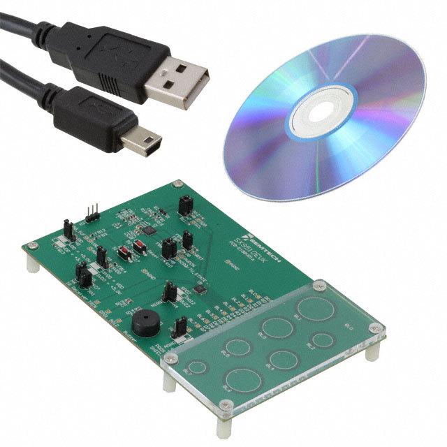
ICGOO在线商城 > 开发板,套件,编程器 > 评估和演示板和套件 > EVB-USB3503

 Datasheet下载
- 型号: EVB-USB3503
- 制造商: Microchip
- 库位|库存: xxxx|xxxx
- 要求:
| 数量阶梯 | 香港交货 | 国内含税 |
| +xxxx | $xxxx | ¥xxxx |
查看当月历史价格
查看今年历史价格
EVB-USB3503产品简介:
ICGOO电子元器件商城为您提供EVB-USB3503由Microchip设计生产,在icgoo商城现货销售,并且可以通过原厂、代理商等渠道进行代购。 EVB-USB3503价格参考。MicrochipEVB-USB3503封装/规格:评估和演示板和套件, USB3503 USB 2.0 Hub Interface Evaluation Board。您可以下载EVB-USB3503参考资料、Datasheet数据手册功能说明书,资料中有EVB-USB3503 详细功能的应用电路图电压和使用方法及教程。
| 参数 | 数值 |
| 品牌 | Microchip Technology |
| 产品目录 | 嵌入式解决方案 |
| 描述 | 界面开发工具 |
| 产品分类 | 工程工具 |
| 产品手册 | |
| 产品图片 |
|
| rohs | 符合RoHS |
| 产品系列 | 模拟与数字IC开发工具,界面开发工具,Microchip Technology EVB-USB3503 |
| mouser_ship_limit | 该产品可能需要其他文件才能进口到中国。 |
| 产品型号 | EVB-USB3503 |
| 产品 | Evaluation Boards |
| 产品种类 | 界面开发工具 |
| 商标 | Microchip Technology |
| 封装 | Bulk |
| 工具用于评估 | USB3503 |
| 接口类型 | USB |
| 描述/功能 | Designed for evaluation of the Microchip USB3503 USB 2.0 HSIC high-speed hub controller |
| 用于 | USB3503 |
| 类型 | USB Hubs |


- 商务部:美国ITC正式对集成电路等产品启动337调查
- 曝三星4nm工艺存在良率问题 高通将骁龙8 Gen1或转产台积电
- 太阳诱电将投资9.5亿元在常州建新厂生产MLCC 预计2023年完工
- 英特尔发布欧洲新工厂建设计划 深化IDM 2.0 战略
- 台积电先进制程称霸业界 有大客户加持明年业绩稳了
- 达到5530亿美元!SIA预计今年全球半导体销售额将创下新高
- 英特尔拟将自动驾驶子公司Mobileye上市 估值或超500亿美元
- 三星加码芯片和SET,合并消费电子和移动部门,撤换高东真等 CEO
- 三星电子宣布重大人事变动 还合并消费电子和移动部门
- 海关总署:前11个月进口集成电路产品价值2.52万亿元 增长14.8%

PDF Datasheet 数据手册内容提取
USB3503 USB 2.0 HSIC High-Speed Hub Controller Optimized for Portable Applications PRODUCT FEATURES Datasheet Features USB Port ESD Protection (DP/DM) Integrated USB 2.0 Compatible 3-Port Hub. — ±15kV (air and contact discharge) — IEC 61000-4-2 level 4 ESD protection without external HSIC Upstream Port devices Advanced power saving features 25-pin WLCS (1.97mm x 1.97mm Wafer Level Chip — 1 μA Typical Standby Current Scale) Package - 0.4mm ball pitch — Port goes into power saving state when no devices are connected downstream Applications — Port is shutdown when port is disabled. — Digital core shut down in Standby Mode The USB3503 is targeted for applications where more Supports either Single-TT or Multi-TT configurations than one USB port is required. As mobile devices add for Full-Speed and Low-Speed connections. more features and the systems become more complex Enhanced configuration options available through it is necessary to have more than one USB port to take serial I2C Slave Port communicate with the internal and peripheral devices. — VID/PID/DID Mobile Phones — String Descriptors Tablet Computers — Configuration options for Hub. Internal Default configuration option when serial I2C Ultra Mobile PCs host not available. Digital Still Cameras MultiTRAKTM Digital Video Camcorders — Dedicated Transaction Translator per port. Gaming Consoles PortMap PDAs — Configurable port mapping and disable sequencing. Portable Media Players PortSwap GPS Personal Navigation Devices — Configurable differential intra-pair signal swapping. Media Players/Viewers PHYBoostTM — Programmable USB transceiver drive strength for recovering signal integrity VariSenseTM — Programmable USB receiver sensitivity flexPWR® Technology — Low current design ideal for battery powered applications — Internal supply switching provides low power modes External 12, 19.2, 24, 25, 26, 27, 38.4, or 52 MHz clock input Internal 3.3V & 1.2V Voltage Regulators for single supply operation. — External VBAT and 1.8V dual supply input option Internal Short Circuit protection of USB differential signal pins. SMSC USB3503A Revision 1.1 (02-07-13) DATASHEET
USB 2.0 HSIC High-Speed Hub Controller Optimized for Portable Applications Datasheet Order Number(s): TEMPERATURE ORDER NUMBER RANGE PACKAGE TYPE REEL SIZE USB3503A-1-GL-TR 0C to 70C 25-Ball WLCSP 3000 pieces USB3503AI-1-GL-TR -40C to 85C 25-Ball WLCSP 3000 pieces This product meets the halogen maximum concentration values per IEC61249-2-21 For RoHS compliance and environmental information, please visit www.smsc.com/rohs Please contact your SMSC sales representative for additional documentation related to this product such as application notes, anomaly sheets, and design guidelines. Copyright © 2013 SMSC or its subsidiaries. All rights reserved. Circuit diagrams and other information relating to SMSC products are included as a means of illustrating typical applications. Consequently, complete information sufficient for construction purposes is not necessarily given. Although the information has been checked and is believed to be accurate, no responsibility is assumed for inaccuracies. SMSC reserves the right to make changes to specifications and product descriptions at any time without notice. Contact your local SMSC sales office to obtain the latest specifications before placing your product order. The provision of this information does not convey to the purchaser of the described semiconductor devices any licenses under any patent rights or other intellectual property rights of SMSC or others. All sales are expressly conditional on your agreement to the terms and conditions of the most recently dated version of SMSC's standard Terms of Sale Agreement dated before the date of your order (the "Terms of Sale Agreement"). The product may contain design defects or errors known as anomalies which may cause the product's functions to deviate from published specifications. Anomaly sheets are available upon request. SMSC products are not designed, intended, authorized or warranted for use in any life support or other application where product failure could cause or contribute to personal injury or severe property damage. Any and all such uses without prior written approval of an Officer of SMSC and further testing and/or modification will be fully at the risk of the customer. Copies of this document or other SMSC literature, as well as the Terms of Sale Agreement, may be obtained by visiting SMSC’s website at http://www.smsc.com. SMSC is a registered trademark of Standard Microsystems Corporation (“SMSC”). Product names and company names are the trademarks of their respective holders. The Microchip name and logo, and the Microchip logo are registered trademarks of Microchip Technology Incorporated in the U.S.A. and other countries. SMSC DISCLAIMS AND EXCLUDES ANY AND ALL WARRANTIES, INCLUDING WITHOUT LIMITATION ANY AND ALL IMPLIED WARRANTIES OF MERCHANTABILITY, FITNESS FOR A PARTICULAR PURPOSE, TITLE, AND AGAINST INFRINGEMENT AND THE LIKE, AND ANY AND ALL WARRANTIES ARISING FROM ANY COURSE OF DEALING OR USAGE OF TRADE. IN NO EVENT SHALL SMSC BE LIABLE FOR ANY DIRECT, INCIDENTAL, INDIRECT, SPECIAL, PUNITIVE, OR CONSEQUENTIAL DAMAGES; OR FOR LOST DATA, PROFITS, SAVINGS OR REVENUES OF ANY KIND; REGARDLESS OF THE FORM OF ACTION, WHETHER BASED ON CONTRACT; TORT; NEGLIGENCE OF SMSC OR OTHERS; STRICT LIABILITY; BREACH OF WARRANTY; OR OTHERWISE; WHETHER OR NOT ANY REMEDY OF BUYER IS HELD TO HAVE FAILED OF ITS ESSENTIAL PURPOSE, AND WHETHER OR NOT SMSC HAS BEEN ADVISED OF THE POSSIBILITY OF SUCH DAMAGES. Revision 1.1 (02-07-13) 2 SMSC USB3503A DATASHEET
USB 2.0 HSIC High-Speed Hub Controller Optimized for Portable Applications Datasheet Table of Contents Chapter1 General Description . . . . . . . . . . . . . . . . . . . . . . . . . . . . . . . . . . . . . . . . . . . . . . . . . . 8 1.1 Customer Selectable Features . . . . . . . . . . . . . . . . . . . . . . . . . . . . . . . . . . . . . . . . . . . . . . . . . . . . . . . 9 1.1.1 Block Diagram . . . . . . . . . . . . . . . . . . . . . . . . . . . . . . . . . . . . . . . . . . . . . . . . . . . . . . . . . . . . . . . . . 10 Chapter2 Acronyms and Definitions . . . . . . . . . . . . . . . . . . . . . . . . . . . . . . . . . . . . . . . . . . . . 11 2.1 Acronyms. . . . . . . . . . . . . . . . . . . . . . . . . . . . . . . . . . . . . . . . . . . . . . . . . . . . . . . . . . . . . . . . . . . . . . . 11 2.2 Reference Documents. . . . . . . . . . . . . . . . . . . . . . . . . . . . . . . . . . . . . . . . . . . . . . . . . . . . . . . . . . . . . 11 Chapter3 USB3503 Pin Definitions . . . . . . . . . . . . . . . . . . . . . . . . . . . . . . . . . . . . . . . . . . . . . 12 3.1 Pin Configuration. . . . . . . . . . . . . . . . . . . . . . . . . . . . . . . . . . . . . . . . . . . . . . . . . . . . . . . . . . . . . . . . . 12 3.2 Signal Definitions. . . . . . . . . . . . . . . . . . . . . . . . . . . . . . . . . . . . . . . . . . . . . . . . . . . . . . . . . . . . . . . . . 12 3.3 Pin Descriptions. . . . . . . . . . . . . . . . . . . . . . . . . . . . . . . . . . . . . . . . . . . . . . . . . . . . . . . . . . . . . . . . . . 14 3.3.1 Pin Definition . . . . . . . . . . . . . . . . . . . . . . . . . . . . . . . . . . . . . . . . . . . . . . . . . . . . . . . . . . . . . . . . . . 14 3.3.2 I/O Type Descriptions. . . . . . . . . . . . . . . . . . . . . . . . . . . . . . . . . . . . . . . . . . . . . . . . . . . . . . . . . . . . 17 3.3.3 Reference Clock. . . . . . . . . . . . . . . . . . . . . . . . . . . . . . . . . . . . . . . . . . . . . . . . . . . . . . . . . . . . . . . . 17 3.3.4 Interrupt . . . . . . . . . . . . . . . . . . . . . . . . . . . . . . . . . . . . . . . . . . . . . . . . . . . . . . . . . . . . . . . . . . . . . 18 Chapter4 Modes of Operation . . . . . . . . . . . . . . . . . . . . . . . . . . . . . . . . . . . . . . . . . . . . . . . . . 20 4.1 Operational Mode Flowchart. . . . . . . . . . . . . . . . . . . . . . . . . . . . . . . . . . . . . . . . . . . . . . . . . . . . . . . . 20 4.2 Standby Mode. . . . . . . . . . . . . . . . . . . . . . . . . . . . . . . . . . . . . . . . . . . . . . . . . . . . . . . . . . . . . . . . . . . 22 4.2.1 External Hardware RESET_N . . . . . . . . . . . . . . . . . . . . . . . . . . . . . . . . . . . . . . . . . . . . . . . . . . . . . 22 4.3 Hub Mode . . . . . . . . . . . . . . . . . . . . . . . . . . . . . . . . . . . . . . . . . . . . . . . . . . . . . . . . . . . . . . . . . . . . . . 22 4.3.1 Hub Initialization Stage (Hub.Init). . . . . . . . . . . . . . . . . . . . . . . . . . . . . . . . . . . . . . . . . . . . . . . . . . . 22 4.3.2 Hub Wait RefClk Stage (Hub.WaitRef). . . . . . . . . . . . . . . . . . . . . . . . . . . . . . . . . . . . . . . . . . . . . . . 22 4.3.3 Hub Configuration Stage (Hub.Config). . . . . . . . . . . . . . . . . . . . . . . . . . . . . . . . . . . . . . . . . . . . . . . 22 4.3.4 Hub Connect Stage (Hub.Connect) . . . . . . . . . . . . . . . . . . . . . . . . . . . . . . . . . . . . . . . . . . . . . . . . . 23 4.3.5 Hub Communication Stage (Hub.Com) . . . . . . . . . . . . . . . . . . . . . . . . . . . . . . . . . . . . . . . . . . . . . . 23 4.3.6 Hub Mode Timing Diagram. . . . . . . . . . . . . . . . . . . . . . . . . . . . . . . . . . . . . . . . . . . . . . . . . . . . . . . . 23 Chapter5 Configuration Options. . . . . . . . . . . . . . . . . . . . . . . . . . . . . . . . . . . . . . . . . . . . . . . 25 5.1 Hub Configuration Options . . . . . . . . . . . . . . . . . . . . . . . . . . . . . . . . . . . . . . . . . . . . . . . . . . . . . . . . . 25 5.1.1 Multi/Single TT . . . . . . . . . . . . . . . . . . . . . . . . . . . . . . . . . . . . . . . . . . . . . . . . . . . . . . . . . . . . . . . . . 25 5.2 Default Serial Interface Register Memory Map. . . . . . . . . . . . . . . . . . . . . . . . . . . . . . . . . . . . . . . . . . 25 5.3 Serial Interface Register Definitions . . . . . . . . . . . . . . . . . . . . . . . . . . . . . . . . . . . . . . . . . . . . . . . . . . 28 5.3.1 Register 00h: Vendor ID (LSB) - VIDL . . . . . . . . . . . . . . . . . . . . . . . . . . . . . . . . . . . . . . . . . . . . . . . 28 5.3.2 Register 01h: Vendor ID (MSB) - VIDM . . . . . . . . . . . . . . . . . . . . . . . . . . . . . . . . . . . . . . . . . . . . . . 28 5.3.3 Register 02h: Product ID (LSB) - PIDL. . . . . . . . . . . . . . . . . . . . . . . . . . . . . . . . . . . . . . . . . . . . . . . 28 5.3.4 Register 03h: Product ID (MSB) - PIDM. . . . . . . . . . . . . . . . . . . . . . . . . . . . . . . . . . . . . . . . . . . . . . 28 5.3.5 Register 04h: Device ID (LSB) - DIDL . . . . . . . . . . . . . . . . . . . . . . . . . . . . . . . . . . . . . . . . . . . . . . . 28 5.3.6 Register 05h: Device ID (MSB) - DIDM . . . . . . . . . . . . . . . . . . . . . . . . . . . . . . . . . . . . . . . . . . . . . . 29 5.3.7 Register 06h: CONFIG_BYTE_1 - CFG1. . . . . . . . . . . . . . . . . . . . . . . . . . . . . . . . . . . . . . . . . . . . . 29 5.3.8 Register 07h: Configuration Data Byte 2 - CFG2. . . . . . . . . . . . . . . . . . . . . . . . . . . . . . . . . . . . . . . 30 5.3.9 Register 08h: Configuration Data Byte 3 - CFG3. . . . . . . . . . . . . . . . . . . . . . . . . . . . . . . . . . . . . . . 30 5.3.10 Register 09h: Non-Removable Device - NRD . . . . . . . . . . . . . . . . . . . . . . . . . . . . . . . . . . . . . . . . 31 5.3.11 Register 0Ah: Port Disable For Self Powered Operation - PDS. . . . . . . . . . . . . . . . . . . . . . . . . . . 31 5.3.12 Register 0Bh: Port Disable For Bus Powered Operation - PDB. . . . . . . . . . . . . . . . . . . . . . . . . . . 32 5.3.13 Register 0Ch: Max Power For Self Powered Operation - MAXPS. . . . . . . . . . . . . . . . . . . . . . . . . 32 5.3.14 Register 0Dh: Max Power For Bus Powered Operation - MAXPB. . . . . . . . . . . . . . . . . . . . . . . . . 32 SMSC USB3503A 3 Revision 1.1 (02-07-13) DATASHEET
USB 2.0 HSIC High-Speed Hub Controller Optimized for Portable Applications Datasheet 5.3.15 Register 0Eh: Hub Controller Max Current For Self Powered Operation - HCMCS. . . . . . . . . . . . 33 5.3.16 Register 0Fh: Hub Controller Max Current For Bus Powered Operation - HCMCB. . . . . . . . . . . . 33 5.3.17 Register 10h: Power-On Time - PWRT . . . . . . . . . . . . . . . . . . . . . . . . . . . . . . . . . . . . . . . . . . . . . 33 5.3.18 Register 11h: Language ID High - LANGIDH. . . . . . . . . . . . . . . . . . . . . . . . . . . . . . . . . . . . . . . . . 33 5.3.19 Register 12h: Language ID Low - LANGIDL . . . . . . . . . . . . . . . . . . . . . . . . . . . . . . . . . . . . . . . . . 34 5.3.20 Register 13h: Manufacturer String Length - MFRSL . . . . . . . . . . . . . . . . . . . . . . . . . . . . . . . . . . . 34 5.3.21 Register 14h: Product String Length - PRDSL. . . . . . . . . . . . . . . . . . . . . . . . . . . . . . . . . . . . . . . . 34 5.3.22 Register 15h: Serial String Length - SERSL. . . . . . . . . . . . . . . . . . . . . . . . . . . . . . . . . . . . . . . . . . 34 5.3.23 Register 16h-53h: Manufacturer String - MANSTR . . . . . . . . . . . . . . . . . . . . . . . . . . . . . . . . . . . . 34 5.3.24 Register 54h-91h: Product String - PRDSTR. . . . . . . . . . . . . . . . . . . . . . . . . . . . . . . . . . . . . . . . . 35 5.3.25 Register 92h-CFh: Serial String - SERSTR . . . . . . . . . . . . . . . . . . . . . . . . . . . . . . . . . . . . . . . . . . 35 5.3.26 Register D0: Downstream Battery Charging Enable - BC_EN. . . . . . . . . . . . . . . . . . . . . . . . . . . . 35 5.3.27 Register E5h: Port Power Status - PRTPWR. . . . . . . . . . . . . . . . . . . . . . . . . . . . . . . . . . . . . . . . . 36 5.3.28 Register E6h: Over Current Sense Control - OCS. . . . . . . . . . . . . . . . . . . . . . . . . . . . . . . . . . . . . 36 5.3.29 Register E7h: Serial Port Interlock Control - SP_ILOCK . . . . . . . . . . . . . . . . . . . . . . . . . . . . . . . . 37 5.3.30 Register E8h: Serial Port Interrupt Status - INT_STATUS. . . . . . . . . . . . . . . . . . . . . . . . . . . . . . . 37 5.3.31 Register E9h: Serial Port Interrupt Mask - INT_MASK. . . . . . . . . . . . . . . . . . . . . . . . . . . . . . . . . . 38 5.3.32 Register EEh: Configure Portable Hub - CFGP . . . . . . . . . . . . . . . . . . . . . . . . . . . . . . . . . . . . . . . 39 5.3.33 Register F4h: Varisense_UP3 - VSNSUP3 . . . . . . . . . . . . . . . . . . . . . . . . . . . . . . . . . . . . . . . . . . 39 5.3.34 Register F5h: Varisense_21 - VSNS21 . . . . . . . . . . . . . . . . . . . . . . . . . . . . . . . . . . . . . . . . . . . . . 40 5.3.35 Register F6h: Boost_Up3 - BSTUP3 . . . . . . . . . . . . . . . . . . . . . . . . . . . . . . . . . . . . . . . . . . . . . . . 40 5.3.36 Register F8h: Boost_21 - BST21 . . . . . . . . . . . . . . . . . . . . . . . . . . . . . . . . . . . . . . . . . . . . . . . . . . 41 5.3.37 Register FAh: Port Swap - PRTSP. . . . . . . . . . . . . . . . . . . . . . . . . . . . . . . . . . . . . . . . . . . . . . . . . 41 5.3.38 Register FBh: Port Remap 12 - PRTR12. . . . . . . . . . . . . . . . . . . . . . . . . . . . . . . . . . . . . . . . . . . . 42 5.3.39 Register FCh: Port Remap 34 - PRTR34. . . . . . . . . . . . . . . . . . . . . . . . . . . . . . . . . . . . . . . . . . . . 43 5.3.40 Register FFh: Status/Command - STCD . . . . . . . . . . . . . . . . . . . . . . . . . . . . . . . . . . . . . . . . . . . . 44 Chapter6 Serial Slave Interface . . . . . . . . . . . . . . . . . . . . . . . . . . . . . . . . . . . . . . . . . . . . . . . . 45 6.1 Overview . . . . . . . . . . . . . . . . . . . . . . . . . . . . . . . . . . . . . . . . . . . . . . . . . . . . . . . . . . . . . . . . . . . . . . . 45 6.2 Interconnecting the USB3503 to an I2C Master . . . . . . . . . . . . . . . . . . . . . . . . . . . . . . . . . . . . . . . . . 45 6.3 I2C Message format . . . . . . . . . . . . . . . . . . . . . . . . . . . . . . . . . . . . . . . . . . . . . . . . . . . . . . . . . . . . . . 46 6.3.1 Sequential Access Writes. . . . . . . . . . . . . . . . . . . . . . . . . . . . . . . . . . . . . . . . . . . . . . . . . . . . . . . . . 46 6.3.2 Sequential Access Reads. . . . . . . . . . . . . . . . . . . . . . . . . . . . . . . . . . . . . . . . . . . . . . . . . . . . . . . . . 46 6.3.3 I2C Timing . . . . . . . . . . . . . . . . . . . . . . . . . . . . . . . . . . . . . . . . . . . . . . . . . . . . . . . . . . . . . . . . . . . . 47 Chapter7 USB Descriptors . . . . . . . . . . . . . . . . . . . . . . . . . . . . . . . . . . . . . . . . . . . . . . . . . . . . 49 7.1 USB Bus Reset . . . . . . . . . . . . . . . . . . . . . . . . . . . . . . . . . . . . . . . . . . . . . . . . . . . . . . . . . . . . . . . . . . 49 7.2 Hub Attached as a High-Speed Device (Customer-Configured for Single-TT Support Only). . . . . . . 49 7.2.1 Standard Device Descriptor . . . . . . . . . . . . . . . . . . . . . . . . . . . . . . . . . . . . . . . . . . . . . . . . . . . . . . . 49 7.2.2 Configuration Descriptor. . . . . . . . . . . . . . . . . . . . . . . . . . . . . . . . . . . . . . . . . . . . . . . . . . . . . . . . . . 50 7.2.3 Interface Descriptor (Single-TT). . . . . . . . . . . . . . . . . . . . . . . . . . . . . . . . . . . . . . . . . . . . . . . . . . . . 51 7.2.4 Endpoint Descriptor (Single-TT). . . . . . . . . . . . . . . . . . . . . . . . . . . . . . . . . . . . . . . . . . . . . . . . . . . . 52 7.3 Hub Attached as a High-Speed Device (Customer-Configured as Multi-TT Capable) . . . . . . . . . . . . 52 7.3.1 Standard Device Descriptor . . . . . . . . . . . . . . . . . . . . . . . . . . . . . . . . . . . . . . . . . . . . . . . . . . . . . . . 52 7.3.2 Configuration Descriptor. . . . . . . . . . . . . . . . . . . . . . . . . . . . . . . . . . . . . . . . . . . . . . . . . . . . . . . . . . 53 7.3.3 Interface Descriptor (Single-TT). . . . . . . . . . . . . . . . . . . . . . . . . . . . . . . . . . . . . . . . . . . . . . . . . . . . 54 7.3.4 Endpoint Descriptor (Single-TT). . . . . . . . . . . . . . . . . . . . . . . . . . . . . . . . . . . . . . . . . . . . . . . . . . . . 55 7.3.5 Interface Descriptor (Multi-TT) . . . . . . . . . . . . . . . . . . . . . . . . . . . . . . . . . . . . . . . . . . . . . . . . . . . . . 55 7.3.6 Endpoint Descriptor (Multi-TT). . . . . . . . . . . . . . . . . . . . . . . . . . . . . . . . . . . . . . . . . . . . . . . . . . . . . 56 7.4 Class-Specific Hub Descriptor. . . . . . . . . . . . . . . . . . . . . . . . . . . . . . . . . . . . . . . . . . . . . . . . . . . . . . . 56 7.5 String Descriptors . . . . . . . . . . . . . . . . . . . . . . . . . . . . . . . . . . . . . . . . . . . . . . . . . . . . . . . . . . . . . . . . 59 7.5.1 String Descriptor Zero (specifies languages supported) . . . . . . . . . . . . . . . . . . . . . . . . . . . . . . . . . 59 SMSC USB3503A 4 Revision 1.1 (02-07-13) DATASHEET
USB 2.0 HSIC High-Speed Hub Controller Optimized for Portable Applications Datasheet 7.5.2 String Descriptor 1 (Manufacturer String). . . . . . . . . . . . . . . . . . . . . . . . . . . . . . . . . . . . . . . . . . . . . 59 7.5.3 String Descriptor 2 (Product String) . . . . . . . . . . . . . . . . . . . . . . . . . . . . . . . . . . . . . . . . . . . . . . . . . 59 7.5.4 String Descriptor 3 (Serial String). . . . . . . . . . . . . . . . . . . . . . . . . . . . . . . . . . . . . . . . . . . . . . . . . . . 60 Chapter8 Battery Charging . . . . . . . . . . . . . . . . . . . . . . . . . . . . . . . . . . . . . . . . . . . . . . . . . . . 61 8.1 Downstream Port Battery Charging Support. . . . . . . . . . . . . . . . . . . . . . . . . . . . . . . . . . . . . . . . . . . . 61 8.1.1 USB Battery Charging . . . . . . . . . . . . . . . . . . . . . . . . . . . . . . . . . . . . . . . . . . . . . . . . . . . . . . . . . . . 61 8.1.2 Special Behavior of PRTPWR Register . . . . . . . . . . . . . . . . . . . . . . . . . . . . . . . . . . . . . . . . . . . . . . 61 8.1.3 Battery Charging Configuration . . . . . . . . . . . . . . . . . . . . . . . . . . . . . . . . . . . . . . . . . . . . . . . . . . . . 62 Chapter9 Integrated Power Regulators. . . . . . . . . . . . . . . . . . . . . . . . . . . . . . . . . . . . . . . . . . 63 9.1 Overview . . . . . . . . . . . . . . . . . . . . . . . . . . . . . . . . . . . . . . . . . . . . . . . . . . . . . . . . . . . . . . . . . . . . . . . 63 9.1.1 3.3V Regulator . . . . . . . . . . . . . . . . . . . . . . . . . . . . . . . . . . . . . . . . . . . . . . . . . . . . . . . . . . . . . . . . . 63 9.1.2 1.2V Regulator . . . . . . . . . . . . . . . . . . . . . . . . . . . . . . . . . . . . . . . . . . . . . . . . . . . . . . . . . . . . . . . . . 63 9.2 Power Configurations . . . . . . . . . . . . . . . . . . . . . . . . . . . . . . . . . . . . . . . . . . . . . . . . . . . . . . . . . . . . . 63 9.2.1 Single Supply Configurations. . . . . . . . . . . . . . . . . . . . . . . . . . . . . . . . . . . . . . . . . . . . . . . . . . . . . . 63 9.2.1.1 VBAT Only. . . . . . . . . . . . . . . . . . . . . . . . . . . . . . . . . . . . . . . . . . . . . . . . . . . . . . . . . . . . . . . . . . . 63 9.2.1.2 3.3V Only. . . . . . . . . . . . . . . . . . . . . . . . . . . . . . . . . . . . . . . . . . . . . . . . . . . . . . . . . . . . . . . . . . . . 63 9.2.2 Double Supply Configurations . . . . . . . . . . . . . . . . . . . . . . . . . . . . . . . . . . . . . . . . . . . . . . . . . . . . . 63 9.2.2.1 VBAT + 1.8V . . . . . . . . . . . . . . . . . . . . . . . . . . . . . . . . . . . . . . . . . . . . . . . . . . . . . . . . . . . . . . . . . 63 9.2.2.2 3.3V + 1.8V . . . . . . . . . . . . . . . . . . . . . . . . . . . . . . . . . . . . . . . . . . . . . . . . . . . . . . . . . . . . . . . . . . 64 9.3 Regulator Control Signals . . . . . . . . . . . . . . . . . . . . . . . . . . . . . . . . . . . . . . . . . . . . . . . . . . . . . . . . . . 64 Chapter10 Specifications. . . . . . . . . . . . . . . . . . . . . . . . . . . . . . . . . . . . . . . . . . . . . . . . . . . . . . 65 10.1 Absolute Maximum Ratings. . . . . . . . . . . . . . . . . . . . . . . . . . . . . . . . . . . . . . . . . . . . . . . . . . . . . . . . 65 10.2 Recommended Operating Conditions. . . . . . . . . . . . . . . . . . . . . . . . . . . . . . . . . . . . . . . . . . . . . . . . 65 10.3 Operating Current . . . . . . . . . . . . . . . . . . . . . . . . . . . . . . . . . . . . . . . . . . . . . . . . . . . . . . . . . . . . . . . 66 10.4 DC Characteristics: Digital I/O Pins. . . . . . . . . . . . . . . . . . . . . . . . . . . . . . . . . . . . . . . . . . . . . . . . . . 68 10.5 DC Characteristics: Analog I/O Pins . . . . . . . . . . . . . . . . . . . . . . . . . . . . . . . . . . . . . . . . . . . . . . . . . 69 10.6 Dynamic Characteristics: Digital I/O Pins . . . . . . . . . . . . . . . . . . . . . . . . . . . . . . . . . . . . . . . . . . . . . 70 10.7 Dynamic Characteristics: Analog I/O Pins. . . . . . . . . . . . . . . . . . . . . . . . . . . . . . . . . . . . . . . . . . . . . 70 10.8 Regulator Output Voltages and Capacitor Requirement. . . . . . . . . . . . . . . . . . . . . . . . . . . . . . . . . . 71 10.9 ESD and Latch-Up Performance. . . . . . . . . . . . . . . . . . . . . . . . . . . . . . . . . . . . . . . . . . . . . . . . . . . . 71 10.10 ESD Performance . . . . . . . . . . . . . . . . . . . . . . . . . . . . . . . . . . . . . . . . . . . . . . . . . . . . . . . . . . . . . . 72 10.10.1 Human Body Model (HBM) Performance. . . . . . . . . . . . . . . . . . . . . . . . . . . . . . . . . . . . . . . . . . . 72 10.10.2 EN 61000-4-2 Performance . . . . . . . . . . . . . . . . . . . . . . . . . . . . . . . . . . . . . . . . . . . . . . . . . . . . . 72 10.10.3 Air Discharge . . . . . . . . . . . . . . . . . . . . . . . . . . . . . . . . . . . . . . . . . . . . . . . . . . . . . . . . . . . . . . . . 72 10.10.4 Contact Discharge . . . . . . . . . . . . . . . . . . . . . . . . . . . . . . . . . . . . . . . . . . . . . . . . . . . . . . . . . . . . 72 10.11 AC Specifications . . . . . . . . . . . . . . . . . . . . . . . . . . . . . . . . . . . . . . . . . . . . . . . . . . . . . . . . . . . . . . 73 10.11.1 REFCLK. . . . . . . . . . . . . . . . . . . . . . . . . . . . . . . . . . . . . . . . . . . . . . . . . . . . . . . . . . . . . . . . . . . . 73 10.11.2 Serial Interface. . . . . . . . . . . . . . . . . . . . . . . . . . . . . . . . . . . . . . . . . . . . . . . . . . . . . . . . . . . . . . . 73 10.11.3 USB 2.0 . . . . . . . . . . . . . . . . . . . . . . . . . . . . . . . . . . . . . . . . . . . . . . . . . . . . . . . . . . . . . . . . . . . . 73 10.11.4 USB 2.0 HSIC. . . . . . . . . . . . . . . . . . . . . . . . . . . . . . . . . . . . . . . . . . . . . . . . . . . . . . . . . . . . . . . . 73 Chapter11 Application Reference . . . . . . . . . . . . . . . . . . . . . . . . . . . . . . . . . . . . . . . . . . . . . . 74 11.1 Application Diagram . . . . . . . . . . . . . . . . . . . . . . . . . . . . . . . . . . . . . . . . . . . . . . . . . . . . . . . . . . . . . 74 Chapter12 Package Outlines, Tape & Reel Drawings, Package Marking. . . . . . . . . . . . . . 77 Chapter13 Datasheet Revision History . . . . . . . . . . . . . . . . . . . . . . . . . . . . . . . . . . . . . . . . . . 82 SMSC USB3503A 5 Revision 1.1 (02-07-13) DATASHEET
USB 2.0 HSIC High-Speed Hub Controller Optimized for Portable Applications Datasheet List of Figures Figure1.1 USB3503 Block Diagram. . . . . . . . . . . . . . . . . . . . . . . . . . . . . . . . . . . . . . . . . . . . . . . . . . . . 10 Figure3.1 USB3503 25-Ball Package. . . . . . . . . . . . . . . . . . . . . . . . . . . . . . . . . . . . . . . . . . . . . . . . . . . 12 Figure3.2 INT_N Operation . . . . . . . . . . . . . . . . . . . . . . . . . . . . . . . . . . . . . . . . . . . . . . . . . . . . . . . . . . 18 Figure4.1 Modes of Operation Flowchart . . . . . . . . . . . . . . . . . . . . . . . . . . . . . . . . . . . . . . . . . . . . . . . 21 Figure4.2 Timing Diagram for Hub Stages. . . . . . . . . . . . . . . . . . . . . . . . . . . . . . . . . . . . . . . . . . . . . . . 24 Figure6.1 I2C Connections. . . . . . . . . . . . . . . . . . . . . . . . . . . . . . . . . . . . . . . . . . . . . . . . . . . . . . . . . . . 45 Figure6.2 I2C Sequential Access Write Format. . . . . . . . . . . . . . . . . . . . . . . . . . . . . . . . . . . . . . . . . . . 46 Figure6.3 Sequential Access Read Format . . . . . . . . . . . . . . . . . . . . . . . . . . . . . . . . . . . . . . . . . . . . . . 47 Figure6.4 I2C Timing Diagram. . . . . . . . . . . . . . . . . . . . . . . . . . . . . . . . . . . . . . . . . . . . . . . . . . . . . . . . 47 Figure8.1 Battery Charging External Power Supply. . . . . . . . . . . . . . . . . . . . . . . . . . . . . . . . . . . . . . . . 61 Figure11.1 Internal Chip-to-Chip Interface. . . . . . . . . . . . . . . . . . . . . . . . . . . . . . . . . . . . . . . . . . . . . . . . 75 Figure11.2 Internal Chip-to-Chip Interface with Embedded Host Port. . . . . . . . . . . . . . . . . . . . . . . . . . . 76 Figure12.1 WLCSP25, 1.97x1.97mm Body, 0.4mm Pitch. . . . . . . . . . . . . . . . . . . . . . . . . . . . . . . . . . . . 77 Figure12.2 WLCSP25, Tape and Reel. . . . . . . . . . . . . . . . . . . . . . . . . . . . . . . . . . . . . . . . . . . . . . . . . . . 78 Figure12.3 WLCSP25, Reel Dimensions. . . . . . . . . . . . . . . . . . . . . . . . . . . . . . . . . . . . . . . . . . . . . . . . . 79 Figure12.4 WLCSP25, Tape Sections. . . . . . . . . . . . . . . . . . . . . . . . . . . . . . . . . . . . . . . . . . . . . . . . . . . 80 Figure12.5 Reflow Profile and Critical Parameters for Lead-free (SnAgCu) Solder. . . . . . . . . . . . . . . . . 80 Figure12.6 Package Marking. . . . . . . . . . . . . . . . . . . . . . . . . . . . . . . . . . . . . . . . . . . . . . . . . . . . . . . . . . 81 SMSC USB3503A 6 Revision 1.1 (02-07-13) DATASHEET
USB 2.0 HSIC High-Speed Hub Controller Optimized for Portable Applications Datasheet List of Tables Table3.1 Pin Descriptions. . . . . . . . . . . . . . . . . . . . . . . . . . . . . . . . . . . . . . . . . . . . . . . . . . . . . . . . . . . . 14 Table3.2 USB3503 I/O Type Descriptions . . . . . . . . . . . . . . . . . . . . . . . . . . . . . . . . . . . . . . . . . . . . . . . 17 Table3.3 USB3503 Primary Reference Clock Frequencies . . . . . . . . . . . . . . . . . . . . . . . . . . . . . . . . . . 17 Table3.4 USB3503 Secondary Reference Clock Frequencies. . . . . . . . . . . . . . . . . . . . . . . . . . . . . . . . 18 Table4.1 Controlling Modes of Operation . . . . . . . . . . . . . . . . . . . . . . . . . . . . . . . . . . . . . . . . . . . . . . . 20 Table4.2 Timing Parameters for Hub Stages. . . . . . . . . . . . . . . . . . . . . . . . . . . . . . . . . . . . . . . . . . . . . 24 Table5.1 Transaction Translator Buffer Chart . . . . . . . . . . . . . . . . . . . . . . . . . . . . . . . . . . . . . . . . . . . . 25 Table5.2 Serial Interface Registers . . . . . . . . . . . . . . . . . . . . . . . . . . . . . . . . . . . . . . . . . . . . . . . . . . . . 26 Table6.1 I2C Timing Specifications . . . . . . . . . . . . . . . . . . . . . . . . . . . . . . . . . . . . . . . . . . . . . . . . . . . . 47 Table7.1 Device Descriptor . . . . . . . . . . . . . . . . . . . . . . . . . . . . . . . . . . . . . . . . . . . . . . . . . . . . . . . . . . 49 Table7.2 Configuration Descriptor (High-Speed, Single-TT Only) . . . . . . . . . . . . . . . . . . . . . . . . . . . . . 50 Table7.3 Interface Descriptor (High-Speed, Single-TT). . . . . . . . . . . . . . . . . . . . . . . . . . . . . . . . . . . . . 51 Table7.4 Endpoint Descriptor (For Status Change Endpoint, Single-TT). . . . . . . . . . . . . . . . . . . . . . . . 52 Table7.5 Device Descriptor (High-Speed) . . . . . . . . . . . . . . . . . . . . . . . . . . . . . . . . . . . . . . . . . . . . . . . 52 Table7.6 Configuration Descriptor (High-Speed) . . . . . . . . . . . . . . . . . . . . . . . . . . . . . . . . . . . . . . . . . . 53 Table7.7 Interface Descriptor (High-Speed, Single-TT). . . . . . . . . . . . . . . . . . . . . . . . . . . . . . . . . . . . . 54 Table7.8 Endpoint Descriptor (For Status Change Endpoint, Single-TT). . . . . . . . . . . . . . . . . . . . . . . . 55 Table7.9 Interface Descriptor (Multi-TT, High-Speed) . . . . . . . . . . . . . . . . . . . . . . . . . . . . . . . . . . . . . . 55 Table7.10EndPoint Descriptor (For Status Change Endpoint, Multi-TT). . . . . . . . . . . . . . . . . . . . . . . . . 56 Table7.11Class-Specific Hub Descriptor . . . . . . . . . . . . . . . . . . . . . . . . . . . . . . . . . . . . . . . . . . . . . . . . 56 Table7.12String Descriptor Zero . . . . . . . . . . . . . . . . . . . . . . . . . . . . . . . . . . . . . . . . . . . . . . . . . . . . . . . 59 Table7.13String Descriptor 1, Manufacturer String. . . . . . . . . . . . . . . . . . . . . . . . . . . . . . . . . . . . . . . . . 59 Table7.14String Descriptor 2, Product String . . . . . . . . . . . . . . . . . . . . . . . . . . . . . . . . . . . . . . . . . . . . . 59 Table7.15String Descriptor 3, Serial String. . . . . . . . . . . . . . . . . . . . . . . . . . . . . . . . . . . . . . . . . . . . . . . 60 Table10.1Absolute Maximum Ratings. . . . . . . . . . . . . . . . . . . . . . . . . . . . . . . . . . . . . . . . . . . . . . . . . . . 65 Table10.2Recommended Operating Conditions . . . . . . . . . . . . . . . . . . . . . . . . . . . . . . . . . . . . . . . . . . . 65 Table10.3Operating Current (Dual Supply). . . . . . . . . . . . . . . . . . . . . . . . . . . . . . . . . . . . . . . . . . . . . . . 66 Table10.4Operating Current (Single Supply). . . . . . . . . . . . . . . . . . . . . . . . . . . . . . . . . . . . . . . . . . . . . . 67 Table10.5Digital I/O Characteristics . . . . . . . . . . . . . . . . . . . . . . . . . . . . . . . . . . . . . . . . . . . . . . . . . . . . 68 Table10.6DC Characteristics: Analog I/O Pins (DP/DM). . . . . . . . . . . . . . . . . . . . . . . . . . . . . . . . . . . . . 69 Table10.7Dynamic Characteristics: Digital I/O Pins (RESET_N) . . . . . . . . . . . . . . . . . . . . . . . . . . . . . . 70 Table10.8Dynamic Characteristics: Analog I/O Pins (DP/DM) . . . . . . . . . . . . . . . . . . . . . . . . . . . . . . . . 70 Table10.9Regulator Output Voltages and Capacitor Requirement. . . . . . . . . . . . . . . . . . . . . . . . . . . . . 71 Table10.10ESD and Latch-up Performance. . . . . . . . . . . . . . . . . . . . . . . . . . . . . . . . . . . . . . . . . . . . . . . 71 Table11.1Component Values in Application Diagrams. . . . . . . . . . . . . . . . . . . . . . . . . . . . . . . . . . . . . . 74 Table11.2Capacitance Values at VBUS of USB Connector . . . . . . . . . . . . . . . . . . . . . . . . . . . . . . . . . . 74 Table13.1Customer Revision History . . . . . . . . . . . . . . . . . . . . . . . . . . . . . . . . . . . . . . . . . . . . . . . . . . . 82 SMSC USB3503A 7 Revision 1.1 (02-07-13) DATASHEET
USB 2.0 HSIC High-Speed Hub Controller Optimized for Portable Applications Datasheet Chapter 1 General Description The SMSC USB3503 is a low-power, USB 2.0 hub controller with HSIC upstream connectivity and three USB 2.0 downtream ports. The USB3503 operates as a hi-speed hub and supports low-speed, full-speed, and hi-speed downstream devices on all of the enabled downstream ports. The USB3503 has been specifically optimized for mobile embedded applications. The pin-count has been reduced by optimizing the USB3503 for mobile battery-powered embedded systems where power consumption, small package size, and minimal BOM are critical design requirements. Standby mode power has been minimized. Instead of a dedicated crystal, reference clock inputs are aligned to mobile applications. Flexible integrated power regulators ease integration into battery powered devices. All required resistors on the USB ports are integrated into the hub. This includes all series termination resistors on D+ and D– pins and all required pull-down resistors on D+ and D– pins. The USB3503 includes programmable features such as: MultiTRAKTM Technology, which utilizes a dedicated Transaction Translator (TT) per port to maintain consistent full-speed data throughput regardless of the number of active downstream connections. MultiTRAKTM outperforms conventional USB 2.0 hubs with a single TT in USB full-speed data transfers. PortMap, which provides flexible port mapping and disable sequences. The downstream ports of a USB3503 hub can be reordered or disabled in any sequence to support multiple platform designs with minimum effort. For any port that is disabled, the USB3503 hub controllers automatically reorder the remaining ports to match the USB host controller’s port numbering scheme. PortSwap, which adds per-port programmability to USB differential-pair pin locations. PortSwap allows direct alignment of USB signals (D+/D-) to connectors to avoid uneven trace length or crossing of the USB differential signals on the PCB. PHYBoost, which provides programmable levels of Hi-Speed USB signal drive strength in the downstream port transceivers. PHYBoost attempts to restore USB signal integrity in a compromised system environment. The graphic on the right shows an example of Hi- Speed USB eye diagrams before and after PHYBoost signal integrity restoration. VariSense, which controls the USB receiver sensitivity enabling programmable levels of USB signal receive sensitivity. This capability allows operation in a sub-optimal system environment, such as when a captive USB cable is used. SMSC USB3503A 8 Revision 1.1 (02-07-13) DATASHEET
USB 2.0 HSIC High-Speed Hub Controller Optimized for Portable Applications Datasheet 1.1 Customer Selectable Features A default configuration is available in the USB3503 following a reset. This configuration may be sufficient for most applications. The USB3503 hub may also be configured by an external microcontroller. When using the microcontroller interface, the hub appears as an I2C slave device. The USB3503 hub supports customer selectable features including: Optional customer configuration via I2C. Supports compound devices on a port-by-port basis. Customizable vendor ID, product ID, and device ID. Configurable downstream port power-on time reported to the host. Supports indication of the maximum current that the hub consumes from the USB upstream port. Supports Indication of the maximum current required for the hub controller. Configurable as a either a Self-Powered or Bus-Powered Hub Supports custom string descriptors (up to 30 characters): — Product string — Manufacturer string — Serial number string When available, I2C configurable options for default configuration may include: — Downstream ports as non-removable ports — Downstream ports as disabled ports — USB signal drive strength — USB receiver sensitivity — USB differential pair pin location SMSC USB3503A 9 Revision 1.1 (02-07-13) DATASHEET
USB 2.0 HSIC High-Speed Hub Controller Optimized for Portable Applications Datasheet 1.1.1 Block Diagram Upstream HSIC To I2C Master Port VBAT VDD_CORE_REG SDA SCL INT_N RESET_N VDD33_BYP VDD12_BYP Mode Serial Control Upstream 3.3V Reg 1.2V Reg Interface - HSIC Standby Hub Mode SIE Controller Repeater TT #1 TT #2 TT #3 Port Controller Routing & Port Re-Ordering Logic PHY#3 PHY#2 PHY#1 PLL USB Data USB Data USB Data REF_CLK HUB_CONNECT Downstream Downstream Downstream Figure1.1 USB3503 Block Diagram SMSC USB3503A 10 Revision 1.1 (02-07-13) DATASHEET
USB 2.0 HSIC High-Speed Hub Controller Optimized for Portable Applications Datasheet Chapter 2 Acronyms and Definitions 2.1 Acronyms EP: Endpoint FS: Full-Speed HS: Hi-Speed I2C®: Inter-Integrated Circuit1 LS: Low-Speed HSIC: High-Speed Inter-Chip 2.2 Reference Documents 1. USB Engineering Change Notice dated December 29th, 2004, UNICODE UTF-16LE For String Descriptors. 2. Universal Serial Bus Specification, Revision 2.0, Dated April 27th, 2000. 3. Battery Charging Specification, Revision 1.1, Release Candidate 10, Dated Sept. 22, 2008 4. High-Speed Inter-Chip USB Electrical Specification, Version 1.0, Dated Sept. 23, 2007 SMSC MAKES NO WARRANTIES, EXPRESS, IMPLIED, OR STATUTORY, IN REGARD TO INFRINGEMENT OR OTHER VIOLATION OF INTELLECTUAL PROPERTY RIGHTS. SMSC DISCLAIMS AND EXCLUDES ANY AND ALL WARRANTIES AGAINST INFRINGEMENT AND THE LIKE. No license is granted by SMSC expressly, by implication, by estoppel or otherwise, under any patent, trademark, copyright, mask work right, trade secret, or other intellectual property right. **To obtain this software program the appropriate SMSC Software License Agreement must be executed and in effect. Forms of these Software License Agreements may be obtained by contacting SMSC. 1. I2C is a registered trademark of Philips Corporation. SMSC USB3503A 11 Revision 1.1 (02-07-13) DATASHEET
USB 2.0 HSIC High-Speed Hub Controller Optimized for Portable Applications Datasheet Chapter 3 USB3503 Pin Definitions 3.1 Pin Configuration The illustration below shows the package diagram. 1 2 3 4 5 A B C D E TOP VIEW Figure3.1 USB3503 25-Ball Package 3.2 Signal Definitions WLCSP PIN NAME DESCRIPTION E2 DATA Upstream HSIC DATA pin of the USB Interface E1 STROBE Upstream HSIC STROBE pin of the USB Interface A5 VDD33_BYP 3.3 V Regulator Bypass C4 PRTPWR Port Power Control Output B4 OCS_N Over Current Sense Input A1 USBDN1_DP USB downstream Port 1 D+ data pin SMSC USB3503A 12 Revision 1.1 (02-07-13) DATASHEET
USB 2.0 HSIC High-Speed Hub Controller Optimized for Portable Applications Datasheet WLCSP PIN NAME DESCRIPTION B1 USBDN1_DM USB downstream Port 1 D- data pin C2 USBDN2_DP USB downstream Port 2 D+ data pin D2 USBDN2_DM USB downstream Port 2 D- data pin C1 USBDN3_DP USB downstream Port 3 D+ data pin D1 USBDN3_DM USB downstream Port 3 D- data pin E5 SCL I2C clock input D5 SDA I2C bi-directional data pin E3 RESET_N Active low reset signal B5 HUB_CONNECT Hub Connect C5 INT_N Active low interrupt signal D4 REF_SEL1 Reference Clock Select 1 input E4 REF_SEL0 Reference Clock Select 0 input B3 REFCLK Reference Clock input A4 RBIAS Bias Resistor pin D3 VDD12_BYP 1.2 V Regulator A2 VDD33_BYP 3.3 V Regulator B2 VBAT Voltage input from the battery supply A3 VDD_CORE_REG Power supply input to 1.2V regulator for digital logic core C3 VSS Ground SMSC USB3503A 13 Revision 1.1 (02-07-13) DATASHEET
USB 2.0 HSIC High-Speed Hub Controller Optimized for Portable Applications Datasheet 3.3 Pin Descriptions This section provides a detailed description of each signal. The signals are arranged in functional groups according to their associated interface. The terms assertion and negation are used. This is done to avoid confusion when working with a mixture of “active low” and “active high” signal. The term “assert”, or “assertion” indicates that a signal is active, independent of whether that level is represented by a high or low voltage. The term “negate”, or “negation” indicates that a signal is inactive. 3.3.1 Pin Definition Table3.1 Pin Descriptions NAME SYMBOL TYPE DESCRIPTION UPSTREAM HIGH SPEED INTER-CHIP INTERFACE HSIC Clock/Strobe STROBE I/O HSIC Upstream Hub Strobe pin HSIC Data DATA I/O HSIC Upstream Hub Data pin High-Speed USB Data USBDN_DP[2:1] A-I/O These pins connect to the downstream USB & & peripheral devices attached to the hub’s ports Port Disable Strap Option USBDN_DM[2:1] Downstream Port Disable Strap option: This pin will be sampled at RESET_N negation to determine if the port is disabled. Both USB data pins for the corresponding port must be tied to VDD33_BYP to disable the associated downstream port. HS USB Data USBDN_DP[3] A-I/O These pins connect to the downstream USB & peripheral devices attached to the hub’s ports. USBDN_DM[3] There is no downstream Port Disable Strap option on these ports. SERIAL PORT INTERFACE Serial Data SDA I/OD I2C Serial Data Serial Clock SCL I Serial Clock (SCL) SMSC USB3503A 14 Revision 1.1 (02-07-13) DATASHEET
USB 2.0 HSIC High-Speed Hub Controller Optimized for Portable Applications Datasheet Table3.1 Pin Descriptions (continued) NAME SYMBOL TYPE DESCRIPTION Interrupt INT_N OD Interrupt The function of this pin is determined by the setting in the CFGP.INTSUSP configuration register. When CFGP.INTSUSP = 0 (General Interrupt) A transition from high to low identifies when one of the interrupt enabled status registers has been updated. SOC must update the Serial Port Interrupt Status Register to reset the interrupt pin high. When CFGP.INTSUSP = 1 (Suspend Interrupt) Indicates USB state of the hub. ‘Asserted’ low = Unconfigured or configured and in USB Suspend ‘Negated’ high = Hub is configured, and is active (i.e., not in suspend) If unused, this pin must be tied to VDD33_BYP. Over Current Sense OCS_N I Over Current Sense - Input from external current monitor indicating an over-current condition on port 3 or on ganged supply. Negated High = No over current fault detected Asserted Low = Over Current Fault Reported Port Power PRTPWR OD Port Power Control- Enables power to USB peripheral devices downstream on port 3 or on ganged supply. Asserted High = External Device should provide power for port(s). Negated Low = External Device should disable power to port(s). MISC Reference Clock Input REFCLK I Reference clock input. Reference Clock Select REF_SEL[1:0] I The reference select input must be set to correspond to the frequency applied to the REFCLK input. The customer should tie these pins to ground or VDD33_BYP. This input is latched during HUB.Init stage. Selects input reference clock frequency per Table3.3. SMSC USB3503A 15 Revision 1.1 (02-07-13) DATASHEET
USB 2.0 HSIC High-Speed Hub Controller Optimized for Portable Applications Datasheet Table3.1 Pin Descriptions (continued) NAME SYMBOL TYPE DESCRIPTION RESET Input RESET_N I This active low signal is used by the system to reset the chip and hold the chip in low power STANDBY MODE. USB Transceiver Bias RBIAS A-I/O A 12.0kΩ (+/- 1%) resistor is attached from ground to this pin to set the transceiver’s internal bias settings. Hub Connect HUB_CONNECT I Hub will transition to the Hub Communication Stage when this pin is asserted high. It can be used in three different ways: Tied to Ground - Hub will not transition to the Hub Communication Stage until connect_n bit of the SP_ILOCK register is negated. Tied to VDD33_BYP - Hub will automatically transition to the Hub Communication Stage regardless of the setting of the connect_n bit and without pausing for the SOC to reference status registers. Transition from low to high - Hub will transition to the Hub Communication Stage after this pin transitions from low to high. HUB_CONNECT should never be driven high when USB3503 is in Standby Mode. POWER 1.2V VDD Power VDD12_BYP Power 1.2 V Regulator. A 1.0 μF (<1 Ω ESR) capacitor to ground is required for regulator stability. The capacitor should be placed as close as possible to the USB3503. 3.3V VDD Power VDD33_BYP Power 3.3V Regulator. A 4.7μF (<1 Ω ESR) capacitor to ground is required for regulator stability. The capacitor should be placed as close as possible to the USB3503. Core Power Supply Input VDD_CORE_REG Power Power supply to 1.2V regulator. This power pin should be connected to VDD33_BYP for single supply applications. Refer to Chapter 9 for power supply configuration options. Battery Power Supply Input VBAT Power Battery power supply. Refer to Chapter 9 for power supply configuration options. VSS VSS Ground Ground SMSC USB3503A 16 Revision 1.1 (02-07-13) DATASHEET
USB 2.0 HSIC High-Speed Hub Controller Optimized for Portable Applications Datasheet 3.3.2 I/O Type Descriptions Table3.2 USB3503 I/O Type Descriptions I/O TYPE DESCRIPTION I Digital Input. OD Digital Output. Open Drain. I/O Digital Input or Output. A-I/O Analog Input or Output. Power DC input or Output. Ground Ground. 3.3.3 Reference Clock The REFCLK input is can be driven with a square wave from 0 V to VDD33_BYP. The USB3503 only uses the positive edge of the clock. The duty cycle is not critical. The USB3503 is tolerant to jitter on the reference clock. The REFCLK jitter should be limited to a peak to peak jitter of less than 1 ns over a 10 μs time interval. If this level of jitter is exceeded the USB3503 high speed eye diagram may be degraded. To select the REFCLK input frequency, the REF_SEL pins must be set according to Table3.3 and Table3.4. To select the primary REFCLK frequencies defined in Table3.3, INT_N must be sampled high during the Hub.Init stage. If the INT_N pin is not used, the INT_N pin should be tied to VDD33_BYP. To select the secondary REFCLK frequencies defined in Table3.4, INT_N must be sampled low during the Hub.Init stage. If the INT_N pin is not used, the INT_N pin should be tied to ground. Since the INT_N pin is open-drain during normal function, selecting the secondary REFCLK frequencies requires that the INT_N pin be driven low from an external source during Hub.Init and then, after startup, that external source must turn into an input to receive the INT_N signal. Table3.3 USB3503 Primary Reference Clock Frequencies REF_SEL[1:0] FREQUENCY (MHz) ‘00’ 38.4 ‘01’ 26.0 ‘10’ 19.2 ‘11’ 12.0 SMSC USB3503A 17 Revision 1.1 (02-07-13) DATASHEET
USB 2.0 HSIC High-Speed Hub Controller Optimized for Portable Applications Datasheet Table3.4 USB3503 Secondary Reference Clock Frequencies REF_SEL[1:0] FREQUENCY (MHz) ‘00’ 24.0 ‘01’ 27.0 ‘10’ 25.0 ‘11’ 50.0 3.3.4 Interrupt The general interrupt pin (INT_N) is intended to communicate a condition change within the hub. The conditions that may cause an interrupt are captured within a register mapped to the serial port (Register E8h: Serial Port Interrupt Status - INT_STATUS). The conditions that cause the interrupt to assert can be controlled through use of an interrupt mask register (Register E9h: Serial Port Interrupt Mask - INT_MASK). The general interrupt and all interrupt conditions are functionally latched and event driven. Once the interrupt or any of the conditions have asserted, the status bit will remain asserted until the SOC negates the bit using the serial port. The bits will then remain negated until a new event condition occurs. The latching nature of the register causes the status to remain even if the condition that caused the interrupt ceases to be active. The event driven nature of the register causes the interrupt to only occur when a new event occurs- when a condition is removed and then is applied again. The function of the interrupt and the associated status and masking registers are illustrated in Figure3.2. Registers & Register bits shown in the figure are defined in Table5.2, “Serial Interface Registers,” on page26. INT_STATUS<4:0> Suspended OR NOT Configured Hub in USB Suspend Mode (SuspInd) SSETQ <4> RCLRQ Hub Configured by USB Host n Port Pow(eHr(u PRbreCtPgowinsrtf)e)r Updated SSRRCCSSEELLRRTTQQQQ n Edge Detectio <<32>> INT_STASTUSETSQ <7> 1 02to1 MUX INT_N o Reserved SSETQ ed RCLR Q s a <1> RCLRQ B et Reserved SSETQ S <0> DSETQ RCLRQ CLRQ CFGP.INTSUSP DSETQ CLRQ INT_MASK SCL/SDA Serial Port Write Logic Figure3.2 INT_N Operation SMSC USB3503A 18 Revision 1.1 (02-07-13) DATASHEET
USB 2.0 HSIC High-Speed Hub Controller Optimized for Portable Applications Datasheet Figure3.2 also shows an alternate configuration option (CFGP.INTSUSP) for a suspend interrupt. This option allows the user to change the behavior of the INT_N pin to become a direct level indication of configuration and suspend status. When selected, the INT_N indicates that the entire hub has entered the USB suspend state. NOTE: Because INT_N is driven low when active, care must be taken when selecting the external pullup resistor value for this open drain output. A sufficiently large resistor must be selected to insure suspend current requirements can be satisfied for the system. SMSC USB3503A 19 Revision 1.1 (02-07-13) DATASHEET
USB 2.0 HSIC High-Speed Hub Controller Optimized for Portable Applications Datasheet Chapter 4 Modes of Operation The USB3503 provides two modes of operation - Standby Mode and Hub Mode - which balance power consumption with functionality. The operating mode of the USB3503 is selected by setting values on primary inputs according to the table below. Table4.1 Controlling Modes of Operation RESET_N RESULTING INPUT MODE SUMMARY 0 Standby Lowest Power Mode – no function other than monitoring RESET_N input to move to higher states. All regulators are powered off. 1 Hub Full Feature Mode - Operates as a configurable USB hub. Power consumption based on how many ports are active, at what speeds they are running and amount of data transferred. 4.1 Operational Mode Flowchart The flowchart in Figure4.1 shows the modes of operation. It also shows how the USB3503 traverses through the Hub mode stages (shown in bold.) The flow of control is dictated by control register bits shown in Italics as well as other events such as availability of reference clock. Refer to Section 5.3, "Serial Interface Register Definitions," on page28 for the detailed definition of the control register bits. In this specification register bits are referenced using the syntax <Register>.<RegisterBit>. A summary of all registers can be found in Table5.2, “Serial Interface Registers,” on page26. The remaining sections in this chapter provide more detail on each stage and mode of operation. SMSC USB3503A 20 Revision 1.1 (02-07-13) DATASHEET
USB 2.0 HSIC High-Speed Hub Controller Optimized for Portable Applications Datasheet Legend Standby Mode Start (SOC Set Pin RESET_N=0) Hub Mode Hub Initialization Stage Core Regulator Enabled Power-On-Reset PLL Synchronization Hub Wait RefClk Stage Wait for Pin HUB_CONNECT=1 OR I2C bit N SP_ILOCK.connect_n=0 REF_CLK available Y Hub Connect Stage Wait for REF_CLK Host Enumerates and Configures Hub Hub Configuration Stage Host Initiates Data Transfers 1 SP_ILOCK. to Downstream Devices config_n 0 System to N power down HSIC I/F Timeout or I2C Write I2C Write SP_ILOCK. config_n=1 Y Wait for I2C bit Timeout SOC Set Pin RESET_N=0 SP_ILOCK.config_n=0 Hub Communication Stage (USB Traffic) Figure4.1 Modes of Operation Flowchart SMSC USB3503A 21 Revision 1.1 (02-07-13) DATASHEET
USB 2.0 HSIC High-Speed Hub Controller Optimized for Portable Applications Datasheet 4.2 Standby Mode Standby Mode provides a very low power state for maximum power efficiency when no signaling is required. This is the lowest power state. In Standby Mode all internal regulators are powered off, the PLL is not running, and core logic is powered down in order to reduce power. Because core logic is powered off, no configuration settings are retained in this mode and must be re-initialized after RESET_N is negated high. 4.2.1 External Hardware RESET_N A valid hardware reset is defined as an assertion of RESET_N low for a minimum of 100us after all power supplies are within operating range. While reset is asserted, the Hub (and its associated external circuitry) enters STANDBY MODE and consumes extremely low current as defined in Table10.3 and Table10.4. Assertion of RESET_N (external pin) causes the following: — All downstream ports are disabled. — All transactions immediately terminate; no states are saved. — All internal registers return to the default state. — The PLL is halted. After RESET_N is negated high in the Hub.Init stage, the Hub reads customer-specific data from the ROM. 4.3 Hub Mode Hub Mode provides functions of configuration and high speed USB hub operation including connection and communication. Upon entering Hub Mode and initializing internal logic, the device passes through several sequential stages based on a fixed time interval. 4.3.1 Hub Initialization Stage (Hub.Init) The first stage is the initialization stage and occurs when Hub mode is entered based on the conditions in Table4.1. In this stage the 1.2V regulator is enabled and stabilizes, internal logic is reset, and the PLL locks if a valid REFCLK is supplied. Configuration registers are initialized to their default state and REF_SEL[1:0] input values are latched. The USB3503 will complete initialization and automatically enter the next stage after T . Because the digital logic within the device is not yet stable, no hubinit communication with the device using the serial port is possible. Configuration registers are initialized to their default state. 4.3.2 Hub Wait RefClk Stage (Hub.WaitRef) During this stage the serial port is not functional. If the reference clock is provided before entering hub mode, the USB3503 will transition to the Hub Configuration stage without pausing in the Hub Wait RefClk stage. Otherwise, the USB3503 will transition to the Hub configuration stage once a valid reference clock is supplied and the PLL has locked. 4.3.3 Hub Configuration Stage (Hub.Config) In this stage, the SOC has an opportunity to control the configuration of the USB3503 and modify any of the default configuration settings specified in the integrated ROM. These settings include USB SMSC USB3503A 22 Revision 1.1 (02-07-13) DATASHEET
USB 2.0 HSIC High-Speed Hub Controller Optimized for Portable Applications Datasheet device descriptors, port electrical settings such as PHY BOOST, and control features. The SOC implements the changes using the serial slave port interface to write configuration & control registers. See Section 5.3.29, "Register E7h: Serial Port Interlock Control - SP_ILOCK," on page37 for definition of SP_ILOCK register and how it controls progress through hub stages. If the SP_ILOCK.config_n bit has its default asserted low and the bit is not written by the serial port, then the USB3503 completes configuration without any I2C intervention. If the SP_ILOCK.config_n bit has its default negated high or the SOC negates the bit high using the serial port during T , the USB3503 will remain in the Hub Configuration Stage indefinitely. This hubconfig will allow the SOC to update other configuration and control registers without any remaining time-out restrictions. Once the SP_ILOCK.config_n bit is asserted low by the SOC the device will transition to the next stage. 4.3.4 Hub Connect Stage (Hub.Connect) Next, the USB3503 enters the Hub Connect Stage. See Section 5.3.32, "Register EEh: Configure Portable Hub - CFGP," on page39 and Section 5.3.29, "Register E7h: Serial Port Interlock Control - SP_ILOCK," on page37 for definition of control registers which affect how the device transitions through the hub stages. By using the appropriate controls, the USB3503 can be set to immediately transition, or instead to remain in the Hub Connect Stage indefinitely until one of the SOC handshake events occur. When set to wait on the handshake, the SOC may read or update any of the serial port registers. Once the SOC finishes accessing registers and is ready for USB communication to start, it can perform one of the selected handshakes which that cause the USB3503 to connect within T and transition to the hubconnect Hub Communication Stage. 4.3.5 Hub Communication Stage (Hub.Com) Once it exits the Hub Connect Stage, the USB3503 enters Hub Communication Stage. In this stage full USB operation is supported under control of the USB Host on the upstream port. The USB3503 will remain in the Hub Communication Stage until the operating mode is changed by the system asserting RESET_N low. While in the Hub Communication Stage, communication over the serial port is no longer supported and the resulting behavior of the serial port if accessed is undefined. In order to re-enable the serial port interface, the device must exit Hub Communication Stage. Exiting this stage is only possible by entering Standby mode. 4.3.6 Hub Mode Timing Diagram The following timing diagram shows the progression through the stages of Hub Mode and the associated timing parameters. SMSC USB3503A 23 Revision 1.1 (02-07-13) DATASHEET
USB 2.0 HSIC High-Speed Hub Controller Optimized for Portable Applications Datasheet RESET_N T_HUBINIT T_HUBCONFIG T_HUBCONNECT Device Standby Hub.Init Hub.Config Hub.Connect Hub.Com Mode.Stage Figure4.2 Timing Diagram for Hub Stages The following table lists the timing parameters associated with the stages of the Hub Mode. Table4.2 Timing Parameters for Hub Stages CHARACTERISTIC SYMBOL MIN TYP MAX UNITS CONDITIONS Hub Initialization T 3 4 ms HUBINIT Time Hub Configuration T 94 95 96 ms HUBCONFIG Time-out Hub Connect Time T 0 1 10 us HUBCONNECT SMSC USB3503A 24 Revision 1.1 (02-07-13) DATASHEET
USB 2.0 HSIC High-Speed Hub Controller Optimized for Portable Applications Datasheet Chapter 5 Configuration Options 5.1 Hub Configuration Options The SMSC Hub supports a number of features (some are mutually exclusive), and must be configured in order to correctly function when attached to a USB host controller. There are two principal ways to configure the hub: by writing to configuration registers using the serial slave port, or by internal default settings. Any configuration registers which are not written by the serial slave retain their default settings. 5.1.1 Multi/Single TT SMSC’s USB 2.0 Hub is fully specification compliant to the Universal Serial Bus Specification Revision 2.0 April 27,2000 (12/7/2000 and 5/28/2002 Errata). Please reference Chapter 11 (Hub Specification) for general details regarding Hub operation and functionality. For performance reasons, the Hub provides 1 Transaction Translator (TT) per port (defined as Multi- TT configuration), and each TT has 1512 bytes of periodic buffer space and 272 Bytes of non- periodic buffer space (divided into 4 non-periodic buffers per TT), for a total of 1784 bytes of buffer space for each Transaction Translator. When configured as a Single-TT Hub (required by USB 2.0 Specification), the Single Transaction Translator will have 1512 bytes of periodic buffer space and 272 bytes of non-periodic buffer space (divided into 4 non-periodic buffers per TT), for a total of 1784 bytes of buffer space for the entire Transaction Translator. Each Transaction Translator’s buffer is divided as shown in Table5.1, "Transaction Translator Buffer Chart". Table5.1 Transaction Translator Buffer Chart Periodic Start-Split Descriptors 256 Bytes Periodic Start-Split Data 752 Bytes Periodic Complete-Split Descriptors 128 Bytes Periodic Complete-Split Data 376 Bytes Non-Periodic Descriptors 16 Bytes Non-Periodic Data 256 Bytes Total for each Transaction Translator 1784 Bytes 5.2 Default Serial Interface Register Memory Map The Serial Interface Registers are used to customize the USB3503 for specific applications. Reserved registers or reserved bits within a defined register should not be written to non-default values or undefined behavior may result. SMSC USB3503A 25 Revision 1.1 (02-07-13) DATASHEET
USB 2.0 HSIC High-Speed Hub Controller Optimized for Portable Applications Datasheet Table5.2 Serial Interface Registers REG ADDR R/W REGISTER NAME ABBREVIATION SECTION 00h R/W VID LSB VIDL 5.3.1, page28 01h R/W VID MSB VIDM 5.3.2, page28 02h R/W PID LSB PIDL 5.3.3, page28 03h R/W PID MSB PIDM 5.3.4, page28 04h R/W DID LSB DIDL 5.3.5, page28 05h R/W DID MSB DIDM 5.3.6, page29 06h R/W Config Data Byte 1 CFG1 5.3.7, page29 07h R/W Config Data Byte 2 CFG2 5.3.8, page30 08h R/W Config Data Byte 3 CFG3 5.3.9, page30 09h R/W Non-Removable Devices NRD 5.3.10, page31 0Ah R/W Port Disable (Self) PDS 5.3.11, page31 0Bh R/W Port Disable (Bus) PDB 5.3.12, page32 0Ch R/W Max Power (Self) MAXPS 5.3.13, page32 0Dh R/W Max Power (Bus) MAXPB 5.3.14, page32 0Eh R/W Hub Controller Max Current HCMCS 5.3.15, page33 (Self) 0Fh R/W Hub Controller Max Current HCMCB 5.3.16, page33 (Bus) 10h R/W Power-on Time PWRT 5.3.17, page33 11h R/W LANG_ID_H LANGIDH 5.3.18, page33 12h R/W LANG_ID_L LANGIDL 5.3.19, page34 13h R/W MFR_STR_LEN MFRSL 5.3.20, page34 14h R/W PRD_STR_LEN PRDSL 5.3.21, page34 15h R/W SER_STR_LEN SERSL 5.3.22, page34 16h- R/W MFR_STR MANSTR 5.3.23, page34 53h 54h- R/W PROD_STR PRDSTR 5.3.24, page35 91h 92h- R/W SER_STR SERSTR 5.3.25, page35 CFh D0h R/W Downstream Battery Charging BC_EN 5.3.26, page35 SMSC USB3503A 26 Revision 1.1 (02-07-13) DATASHEET
USB 2.0 HSIC High-Speed Hub Controller Optimized for Portable Applications Datasheet Table5.2 Serial Interface Registers (continued) REG ADDR R/W REGISTER NAME ABBREVIATION SECTION D1-E1h R/W Reserved N/A E2h R/W Reserved N/A E3-E4h R/W Reserved N/A E5h R Port Power Status PRTPWR 5.3.27, page36 E6h R/W Over Current Sense Control OCS 5.3.28, page36 E7h R/W Serial Port Interlock Control SP_ILOCK 5.3.29, page37 E8h R/W Serial Port Interrupt Status INT_STATUS 5.3.30, page37 E9h R/W Serial Port Interrupt Mask INT_MASK 5.3.31, page38 EAh- R/W Reserved N/A EDh EEh R/W Configure Portable Hub CFGP 5.3.32, page39 EFh- R Reserved N/A F3h F4h R/W Varisense_Up3 VSNSUP3 5.3.33, page39 F5h R/W Varisense_21 VSNS21 5.3.34, page40 F6h R/W Boost_Up3 BSTUP3 5.3.35, page40 F7h R/W Reserved N/A F8h R/W Boost_21 BST21 5.3.36, page41 F9h R/W Reserved N/A FAh R/W Port Swap PRTSP 5.3.37, page41 FBh R/W Port Remap 12 PRTR12 5.3.38, page42 FCh R/W Port Remap 34 PRTR34 5.3.39, page43 FDh R/W Reserved N/A FEh R/W Reserved N/A FFh R/W I2C Status/Command STCD 5.3.40, page44 SMSC USB3503A 27 Revision 1.1 (02-07-13) DATASHEET
USB 2.0 HSIC High-Speed Hub Controller Optimized for Portable Applications Datasheet 5.3 Serial Interface Register Definitions 5.3.1 Register 00h: Vendor ID (LSB) - VIDL Default = 0x24h - Corresponds to SMSC Vendor ID. BIT NUMBER BIT NAME DESCRIPTION 7:0 VID_LSB Least Significant Byte of the Vendor ID. This is a 16-bit value that uniquely identifies the Vendor of the user device (assigned by USB-Interface Forum). This field is set by the customer using the serial interface options. 5.3.2 Register 01h: Vendor ID (MSB) - VIDM Default = 0x04h - Corresponds to SMSC Vendor ID. BIT NUMBER BIT NAME DESCRIPTION 7:0 VID_MSB Most Significant Byte of the Vendor ID. This is a 16-bit value that uniquely identifies the Vendor of the user device (assigned by USB-Interface Forum). This field is set by the customer using serial interface options. 5.3.3 Register 02h: Product ID (LSB) - PIDL Default = 0x03h - Corresponds to SMSC USB part number for 3-port device. BIT NUMBER BIT NAME DESCRIPTION 7:0 PID_LSB Least Significant Byte of the Product ID. This is a 16-bit value that the Vendor can assign that uniquely identifies this particular product (assigned by customer). This field is set by the customer using the serial interface options. 5.3.4 Register 03h: Product ID (MSB) - PIDM Default = 0x35h Corresponds to SMSC 3503 device. BIT NUMBER BIT NAME DESCRIPTION 7:0 PID_MSB Most Significant Byte of the Product ID. This is a 16-bit value that the Vendor can assign that uniquely identifies this particular product (assigned by customer). This field is set by the customer using the serial interface options. 5.3.5 Register 04h: Device ID (LSB) - DIDL Default = 0xA0h BIT NUMBER BIT NAME DESCRIPTION 7:0 DID_LSB Least Significant Byte of the Device ID. This is a 16-bit device release number in BCD format (assigned by customer). This field is set by the customer using the serial interface options. SMSC USB3503A 28 Revision 1.1 (02-07-13) DATASHEET
USB 2.0 HSIC High-Speed Hub Controller Optimized for Portable Applications Datasheet 5.3.6 Register 05h: Device ID (MSB) - DIDM Default = 0xA1h BIT NUMBER BIT NAME DESCRIPTION 7:0 DID_MSB Most Significant Byte of the Device ID. This is a 16-bit device release number in BCD format (assigned by customer). This field is set by the customer using the serial interface options. 5.3.7 Register 06h: CONFIG_BYTE_1 - CFG1 Default = 0x98h - Corresponds to Self Powered, Ganged Port Power BIT NUMBER BIT NAME DESCRIPTION 7 SELF_BUS_PW Self or Bus Power: Selects between Self- and Bus-Powered operation. R The Hub is either Self-Powered or Bus-Powered. When configured as a Bus-Powered device, the SMSC Hub consumes less than 100mA of current prior to being configured. After configuration, the Bus-Powered SMSC Hub (along with all associated hub circuitry, any embedded devices if part of a compound device, and 100mA per externally available downstream port) must consume no more than 500mA of upstream VBUS current. The current consumption is system dependent, and the customer must ensure that the USB 2.0 specifications are not violated. When configured as a Self-Powered device, <1mA of upstream VBUS current is consumed and all ports are available, with each port being capable of sourcing 500mA of current. This field is set by the customer using the serial interface options. 0 = Bus-Powered operation. 1 = Self-Powered operation. 6 Reserved Reserved 5 Reserved Reserved 4 MTT_ENABLE Multi-TT enable: Enables one transaction translator per port operation. Selects between a mode where only one transaction translator is available for all ports (Single-TT), or each port gets a dedicated transaction translator (Multi- TT) {Note: The host may force Single-TT mode only}. 0 = single TT for all ports. 1 = one TT per port (multiple TT’s supported) 3 Reserved Reserved 2:1 CURRENT_SNS Over Current Sense: Selects current sensing on a port-by-port basis, all ports ganged, or none (only for bus-powered hubs) The ability to support current sensing on a port or ganged basis is hardware implementation dependent. 00 = Ganged sensing (all ports together). 01 = Individual port-by-port. 1x = Over current sensing not supported. (must only be used with Bus- Powered configurations!) 0 PORT_PWR Port Power Switching: Enables power switching on all ports simultaneously (ganged), or port power is individually switched on and off on a port- by-port basis (individual). The ability to support power enabling on a port or ganged basis is hardware implementation dependent. 0 = Ganged switching (all ports together) 1 = Individual port-by-port switching. SMSC USB3503A 29 Revision 1.1 (02-07-13) DATASHEET
USB 2.0 HSIC High-Speed Hub Controller Optimized for Portable Applications Datasheet 5.3.8 Register 07h: Configuration Data Byte 2 - CFG2 Default = 0x20h - Not a Compound Device BIT NUMBER BIT NAME DESCRIPTION 7:4 Reserved Reserved 3 COMPOUND Compound Device: Allows the customer to indicate that the Hub is part of a compound (see the USB Specification for definition) device. The applicable port(s) must also be defined as having a “Non-Removable Device”. 0 = No. 1 = Yes, Hub is part of a compound device. 2:0 Reserved Reserved 5.3.9 Register 08h: Configuration Data Byte 3 - CFG3 Default = 0x03h BIT NUMBER BIT NAME DESCRIPTION 7:4 Reserved Reserved 3 PRTMAP_EN Port Re-Mapping enable: Selects the method used by the hub to assign port numbers and disable ports ‘0’ = Standard Mode. The following registers are used to define which ports are enabled, and the ports are mapped as Port “n” on the hub is reported as Port ‘n’ to the host, unless one of the ports is disabled, then the higher numbered ports are remapped in order to report contiguous port numbers to the host. Section5.3.11 Register 0A Section5.3.12 Register 0B ‘1’ = Port Re-Map mode. The mode enables remapping via the registers defined below. Section5.3.38 Register FB Section5.3.39 Register FC 2:1 Reserved Reserved 0 STRING_EN Enables String Descriptor Support ‘0’ = String Support Disabled ‘1’ = String Support Enabled SMSC USB3503A 30 Revision 1.1 (02-07-13) DATASHEET
USB 2.0 HSIC High-Speed Hub Controller Optimized for Portable Applications Datasheet 5.3.10 Register 09h: Non-Removable Device - NRD Default = 0x00h BIT NUMBER BIT NAME DESCRIPTION 7:0 NR_DEVICE Non-Removable Device: Indicates which port(s) include non- removable devices. ‘0’ = port is removable ‘1’ = port is non- removable. Informs the Host if one of the active physical ports has a permanent device that is undetachable from the Hub. (Note: The device must provide its own descriptor data.) Bit 7= Reserved Bit 6= Reserved Bit 5= Reserved Bit 4= Reserved Bit 3= Port 3 non-removable. Bit 2= Port 2 non-removable. Bit 1= Port 1 non removable. Bit 0= Reserved 5.3.11 Register 0Ah: Port Disable For Self Powered Operation - PDS Default = 0x00h BIT NUMBER BIT NAME DESCRIPTION 7:0 PORT_DIS_SP Port Disable, Self-Powered: Disables 1 or more ports. ‘0’ = port is available ‘1’ = port is disabled. During Self-Powered operation and PRTMAP_EN = ‘0’, this selects the ports which will be permanently disabled, and are not available to be enabled or enumerated by a Host Controller. The ports can be disabled in any order, the internal logic will automatically report the correct number of enabled ports to the USB Host, and will reorder the active ports in order to ensure proper function. Bit 7= Reserved Bit 6= Reserved Bit 5= Reserved Bit 4= Reserved Bit 3= Port 3 Disable. Bit 2= Port 2 Disable. Bit 1= Port 1 Disable. Bit 0= Reserved SMSC USB3503A 31 Revision 1.1 (02-07-13) DATASHEET
USB 2.0 HSIC High-Speed Hub Controller Optimized for Portable Applications Datasheet 5.3.12 Register 0Bh: Port Disable For Bus Powered Operation - PDB Default = 0x00h BIT NUMBER BIT NAME DESCRIPTION 7:0 PORT_DIS_BP Port Disable, Bus-Powered: Disables 1 or more ports. ‘0’ = port is available ‘1’ = port is disabled. During Bus-Powered operation and PRTMAP_EN = ‘0’, this selects the ports which will be permanently disabled, and are not available to be enabled or enumerated by a Host Controller. The ports can be disabled in any order, the internal logic will automatically report the correct number of enabled ports to the USB Host, and will reorder the active ports in order to ensure proper function. Bit 7= Reserved Bit 6= Reserved Bit 5= Reserved Bit 4= Reserved Bit 3= Port 3 Disable. Bit 2= Port 2 Disable. Bit 1= Port 1 Disable. Bit 0= Reserved 5.3.13 Register 0Ch: Max Power For Self Powered Operation - MAXPS Default = 0x01h BIT NUMBER BIT NAME DESCRIPTION 7:0 MAX_PWR_SP Max Power Self_Powered: Value in 2mA increments that the Hub consumes from an upstream port when operating as a self-powered hub. This value includes the hub silicon along with the combined power consumption (from VBUS) of all associated circuitry on the board. This value also includes the power consumption of a permanently attached peripheral if the hub is configured as a compound device, and the embedded peripheral reports 0mA in its descriptors. Example: A value of 8mA would be written to this register as 0x04h Note: The USB 2.0 Specification does not permit this value to exceed 100mA 5.3.14 Register 0Dh: Max Power For Bus Powered Operation - MAXPB Default = 0xFAh- Corresponds to 500mA. BIT NUMBER BIT NAME DESCRIPTION 7:0 MAX_PWR_BP Max Power Bus_Powered: Value in 2mA increments that the Hub consumes from an upstream port when operating as a bus-powered hub. This value includes the hub silicon along with the combined power consumption (from VBUS) of all associated circuitry on the board. This value also includes the power consumption of a permanently attached peripheral if the hub is configured as a compound device, and the embedded peripheral reports 0mA in its descriptors. Example: A value of 8mA would be written to this register as 0x04h SMSC USB3503A 32 Revision 1.1 (02-07-13) DATASHEET
USB 2.0 HSIC High-Speed Hub Controller Optimized for Portable Applications Datasheet 5.3.15 Register 0Eh: Hub Controller Max Current For Self Powered Operation - HCMCS Default = 0x02h Corresponds to 2mA. BIT NUMBER BIT NAME DESCRIPTION 7:0 HC_MAX_C_SP Hub Controller Max Current Self-Powered: Value in 1mA increments that the Hub consumes from an upstream port when operating as a self- powered hub. This value includes the hub silicon along with the combined power consumption (from VBUS) of all associated circuitry on the board. This value does NOT include the power consumption of a permanently attached peripheral if the hub is configured as a compound device. Example: A value of 8mA would be written to this register as 0x08h Note: The USB 2.0 Specification does not permit this value to exceed 100mA 5.3.16 Register 0Fh: Hub Controller Max Current For Bus Powered Operation - HCMCB Default = 0x64h- Corresponds to 100mA. BIT NUMBER BIT NAME DESCRIPTION 7:0 HC_MAX_C_BP Hub Controller Max Current Bus-Powered: Value in 1mA increments that the Hub consumes from an upstream port when operating as a bus- powered hub. Example: A value of 8mA would be written to this register as 0x08h 5.3.17 Register 10h: Power-On Time - PWRT Default = 0x00h - Corresponds to 0ms. Required for a hub with no power switches BIT NUMBER BIT NAME DESCRIPTION 7:0 POWER_ON_TI Power On Time: The length of time that is takes (in 2 ms intervals) from the time ME the host initiated power-on sequence begins on a port until power is good on that port. System software uses this value to determine how long to wait before accessing a powered-on port. Setting affects only the hub descriptor field “PwrOn2PwrGood” see Section 7.4, "Class-Specific Hub Descriptor," on page56. Note: This register represents time from when a host sends a SetPortFeature(PORT_POWER) request to the time power is supplied through an external switch to a downstream port. It should be set to 0 if no power switch is used- for instance within a compound device. 5.3.18 Register 11h: Language ID High - LANGIDH Default = 0x04h - Corresponds to US English code 0x0409h BIT NUMBER BIT NAME DESCRIPTION 7:0 LANG_ID_H USB LANGUAGE ID (Upper 8 bits of a 16 bit ID field) SMSC USB3503A 33 Revision 1.1 (02-07-13) DATASHEET
USB 2.0 HSIC High-Speed Hub Controller Optimized for Portable Applications Datasheet 5.3.19 Register 12h: Language ID Low - LANGIDL Default = 0x09h - Corresponds to US English code 0x0409h BIT NUMBER BIT NAME DESCRIPTION 7:0 LANG_ID_L USB LANGUAGE ID (lower 8 bits of a 16 bit ID field) 5.3.20 Register 13h: Manufacturer String Length - MFRSL Default = 0x00h BIT NUMBER BIT NAME DESCRIPTION 7:0 MFR_STR_LEN Manufacturer String Length 5.3.21 Register 14h: Product String Length - PRDSL Default = 0x00h BIT NUMBER BIT NAME DESCRIPTION 7:0 PRD_STR_LEN Product String Length 5.3.22 Register 15h: Serial String Length - SERSL Default = 0x00h BIT NUMBER BIT NAME DESCRIPTION 7:0 SER_STR_LEN Serial String Length 5.3.23 Register 16h-53h: Manufacturer String - MANSTR Default = 0x00h BIT NUMBER BIT NAME DESCRIPTION 7:0 MFR_STR Manufacturer String, UNICODE UTF-16LE per USB 2.0 Specification Note: The String consists of individual 16 Bit UNICODE UTF-16LE characters. The Characters will be stored starting with the LSB at the least significant address and the MSB at the next 8-bit location (subsequent characters must be stored in sequential contiguous address in the same LSB, MSB manner). Please pay careful attention to the Byte ordering or your selected programming tools. SMSC USB3503A 34 Revision 1.1 (02-07-13) DATASHEET
USB 2.0 HSIC High-Speed Hub Controller Optimized for Portable Applications Datasheet 5.3.24 Register 54h-91h: Product String - PRDSTR Default = 0x00h BIT NUMBER BIT NAME DESCRIPTION 7:0 PRD_STR Product String, UNICODE UTF-16LE per USB 2.0 Specification Note: The String consists of individual 16 Bit UNICODE UTF-16LE characters. The Characters will be stored starting with the LSB at the least significant address and the MSB at the next 8-bit location (subsequent characters must be stored in sequential contiguous address in the same LSB, MSB manner). Please pay careful attention to the Byte ordering or your selected programming tools. 5.3.25 Register 92h-CFh: Serial String - SERSTR Default = 0x00h BIT NUMBER BIT NAME DESCRIPTION 7:0 SER_STR Serial String, UNICODE UTF-16LE per USB 2.0 Specification Note: The String consists of individual 16 Bit UNICODE UTF-16LE characters. The Characters will be stored starting with the LSB at the least significant address and the MSB at the next 8-bit location (subsequent characters must be stored in sequential contiguous address in the same LSB, MSB manner). Please pay careful attention to the Byte ordering or your selected programming tools. 5.3.26 Register D0: Downstream Battery Charging Enable - BC_EN Default = 0x00h BIT NUMBER BIT NAME DESCRIPTION 7:0 BC_EN Battery Charging Enable: Enables the battery charging feature for the corresponding downstream port. ‘0’ = Downstream Battery Charging support is not enabled. ‘1’ = Downstream Battery charging support is enabled Bit 7= Reserved Bit 6= Reserved Bit 5= Reserved Bit 4= Reserved Bit 3= Port 3 Battery Charging Enable. Bit 2= Port 2 Battery Charging Enable. Bit 1= Port 1 Battery Charging Enable. Bit 0= Reserved SMSC USB3503A 35 Revision 1.1 (02-07-13) DATASHEET
USB 2.0 HSIC High-Speed Hub Controller Optimized for Portable Applications Datasheet 5.3.27 Register E5h: Port Power Status - PRTPWR Default = 0x00h BIT NUMBER BIT NAME DESCRIPTION 7:4 Reserved Reserved. 3:1 PRTPWR[3:1] Read Only. Optional status to SOC indicating that power to the downstream port was enabled by the USB Host for the specified port. Not required for an embedded application. This is a read-only status bit. Actual control over port power is implemented by the USB Host, OCS register and Downstream Battery Charging logic if enabled. See Section 8.1.2, "Special Behavior of PRTPWR Register," on page61 for more information. 0 = USB Host has not enabled port to be powered or in downstream battery charging and corresponding OCS bit has been set. 1 = USB Host has enabled port to be powered 0 Reserved Reserved. 5.3.28 Register E6h: Over Current Sense Control - OCS Default = 0x00h BIT NUMBER BIT NAME DESCRIPTION 7:4 Reserved Reserved. {Note: Software must never write a ‘1’ to these bits} 3 OCS[3] When SP_ILOCK.OcsPinSel = 1 Register Bit is reserved. Setting bit has no effect on HUB operation, instead OCS_N device pin controls over current condition reporting. When SP_ILOCK.OcsPinSel = 0 Optional control from SOC on indicating external current monitor indicating an over-current condition on port 3 for HUB status reporting to USB host. Also resets corresponding PRTPWR status register bit. Not required for an embedded application. 0 = No Over Current Condition 1 = Over Current Condition 2:1 OCS[2:1] Optional control from SOC on indicating external current monitor indicating an over-current condition on the specified port for HUB status reporting to USB host. Also resets corresponding PRTPWR status register bit. Not required for an embedded application. 0 = No Over Current Condition 1 = Over Current Condition 0 Reserved Reserved. SMSC USB3503A 36 Revision 1.1 (02-07-13) DATASHEET
USB 2.0 HSIC High-Speed Hub Controller Optimized for Portable Applications Datasheet 5.3.29 Register E7h: Serial Port Interlock Control - SP_ILOCK Default=0x32h - Corresponds to OCS_N/PRT_PWR pins & pausing to connect until write from I2C BIT NUMBER BIT NAME DESCRIPTION 7:6 Reserved Reserved 5 OcsPinSel 1= OCS device pin will assume role as an active low Over Current Sense input 0= OCS device pin disabled, register control established 4 PrtPwrPinSel 1=PRTPWR device pin will assume role as an active high Port Power Switch Control output 0=PRTPWR device pin disabled, register control established 3:2 Reserved Reserved 1 connect_n The SOC can utilize this bit to control when the hub attempts to connect to the upstream host. 1 = Device will remain in Hub Mode.Connect Stage indefinitely until bit is cleared by the SOC. 0 = Device will transition to the Hub Mode.Communication Stage after this bit is asserted low by default or through a serial port write. 0 config_n If the SOC intends to update the default configuration using the serial port, this register should be the first register updated by the SOC. In this way the timing dependency between configuration and device operation can be minimized- the SOC is only required to write to Serial Port Interlock Register within T hubconfig and not all the registers it is attempting to configure. Once all registers have been written for the desired configuration, the SOC must clear this bit to ‘0’ for the device to resume normal operation using the new configuration. It may be desirable for the device to initiate autonomous operation with no SOC intervention at all. This is why the default setting is to allow the device to initiate automatic operation if the SOC does not intervene by writing the interlock register within the allotted configuration timeout. 1 = Device will remain in Hub Mode.Configuration Stage indefinitely, and allow SOC to write through the serial port to set any desired configuration. 0 = Device will transition out of Hub.Configuration Stage immediately after this bit is asserted low through a serial port write. (A default low assertion results in transition after a timeout.) 5.3.30 Register E8h: Serial Port Interrupt Status - INT_STATUS Default = 0x00h BIT NUMBER BIT NAME DESCRIPTION 7 Interrupt Read: 1 = INT_N pin has been asserted low due to unmasked interrupt 0 = INT_N pin has not been asserted low due to unmasked interrupt Write: 1 = No Effect – INT_N pin and register retains its current value 0 = Negate INT_N pin high 6:5 Reserved Reserved SMSC USB3503A 37 Revision 1.1 (02-07-13) DATASHEET
USB 2.0 HSIC High-Speed Hub Controller Optimized for Portable Applications Datasheet BIT NUMBER BIT NAME DESCRIPTION 4 HubSuspInt Read: 1 = Hub has entered USB suspend 0 = Hub has not entered USB suspend since last HubSuspInt reset Write: 1 = No Effect 0 = Negate HubSuspInt status low 3 HubCfgInt Read: 1 = Hub has been configured by USB Host 0 = Hub has not been configured by USB Host since last HubConfInt reset Write: 1 = No Effect 0 = Negate HubConfInt status low 2 PrtPwrInt Read: 1 = Port Power register has been updated 0 = Port Power register has not been updated since last PrtPwrInt reset Write: 1 = No Effect 0 = Negate PrtPwrInt status low 1:0 Reserved Reserved 5.3.31 Register E9h: Serial Port Interrupt Mask - INT_MASK Default = 0x00h BIT NUMBER BIT NAME DESCRIPTION 7:5 Reserved Reserved 4 HubSuspMask 1 = INT_N pin is asserted low when Hub enters suspend 0 = INT_N pin is not affected by Hub entering suspend 3 HubCfgMask 1 = INT_N pin is asserted low when Hub configured by USB Host 0 = INT_N pin is not affected by Hub configuration event 2 PrtPwrMask 1 = INT_N pin is asserted low when Port Power register has been updated by USB Host 0 = INT_N pin is not affected by Port Power register 1:0 Reserved Reserved SMSC USB3503A 38 Revision 1.1 (02-07-13) DATASHEET
USB 2.0 HSIC High-Speed Hub Controller Optimized for Portable Applications Datasheet 5.3.32 Register EEh: Configure Portable Hub - CFGP Default = 0x00h - Corresponds to 95ms startup & Phone RefClks available BIT NUMBER BIT NAME DESCRIPTION 7 ClkSusp (Read/Write) 1 = Force device to run internal clock even during USB suspend (will cause device to violate USB suspend current limit - intended for test or self-powered applications which require use of serial port during USB session.) 0 = Allow device to gate off its internal clocks during suspend mode in order to meet USB suspend current requirements. 6 IntSusp (Read/Write) 1 = INT_N pin function is a level sensitive USB suspend interrupt indication. Allows system to adjust current consumption to comply with USB specification limits when hub is in the USB suspend state. 0 = INT_N pin function retains event sensitive role of a general serial port interrupt. See Section 3.3.4, "Interrupt," on page18 for more information. 5:4 CfgTout (Read Only) Specifies timeout value for allowing SOC to configure the device. Corresponds to the T parameter. See Section Table4.2, "Timing Parameters for Hub hubconfig Stages". ‘00’ = 95ms - Use to meet legacy 100ms connect timing 3 Reserved Reserved 2:0 Reserved Reserved 5.3.33 Register F4h: Varisense_UP3 - VSNSUP3 Default = 0x00h BIT NUMBER BIT NAME DESCRIPTION 7:3 Reserved Reserved 2:0 DN3_SQUELCH These two bits control the Squelch setting of the downstream port 3. ‘000’ = Nominal value ‘001’ = 90% of Nominal value ‘010’ = 80% of Nominal value ‘011’ = 70% of Nominal value ‘100’ = 60% of Nominal value ‘101’ = 50% of Nominal value ‘110’ = 120% of Nominal value ‘111’ = 110% of Nominal value SMSC USB3503A 39 Revision 1.1 (02-07-13) DATASHEET
USB 2.0 HSIC High-Speed Hub Controller Optimized for Portable Applications Datasheet 5.3.34 Register F5h: Varisense_21 - VSNS21 Default = 0x00h BIT NUMBER BIT NAME DESCRIPTION 7 Reserved Reserved 6:4 DN2_SQUELCH These two bits control the Squelch setting of the downstream port 2. ‘000’ = Nominal value ‘001’ = 90% of Nominal value ‘010’ = 80% of Nominal value ‘011’ = 70% of Nominal value ‘100’ = 60% of Nominal value ‘101’ = 50% of Nominal value ‘110’ = 120% of Nominal value ‘111’ = 110% of Nominal value 3 Reserved Reserved 2:0 DN1_SQUELCH These three bits control the Squelch setting of the downstream port 1. ‘000’ = Nominal value ‘001’ = 90% of Nominal value ‘010’ = 80% of Nominal value ‘011’ = 70% of Nominal value ‘100’ = 60% of Nominal value ‘101’ = 50% of Nominal value ‘110’ = 120% of Nominal value ‘111’ = 110% of Nominal value 5.3.35 Register F6h: Boost_Up3 - BSTUP3 Default = 0x30h BIT NUMBER BIT NAME DESCRIPTION 7:3 Reserved Reserved 2:0 BOOST_IOUT_3 USB electrical signaling drive strength Boost Bit for Downstream Port ‘3’. Boosts USB High Speed Current. 3’b000: Nominal 3’b001: -5% 3’b010: +10% 3’b011: +5% 3’b100: +20% 3’b101: +15% 3’b110: +30% 3’b111: +25% SMSC USB3503A 40 Revision 1.1 (02-07-13) DATASHEET
USB 2.0 HSIC High-Speed Hub Controller Optimized for Portable Applications Datasheet 5.3.36 Register F8h: Boost_21 - BST21 Default = 0x00h BIT NUMBER BIT NAME DESCRIPTION 7 Reserved Reserved 6:4 BOOST_IOUT_2 USB electrical signaling drive strength Boost Bit for Downstream Port ‘2’. Boosts USB High Speed Current. 3’b000: Nominal 3’b001: -5% 3’b010: +10% 3’b011: +5% 3’b100: +20% 3’b101: +15% 3’b110: +30% 3’b111: +25% 3 Reserved Reserved 2:0 BOOST_IOUT_1 USB electrical signaling drive strength Boost Bit for Downstream Port ‘1’. Boosts USB High Speed Current. 3’b000: Nominal 3’b001: -5% 3’b010: +10% 3’b011: +5% 3’b100: +20% 3’b101: +15% 3’b110: +30% 3’b111: +25% 5.3.37 Register FAh: Port Swap - PRTSP Default = 0x00h BIT NUMBER BIT NAME DESCRIPTION 7:0 PRTSP Port Swap: Swaps the Upstream HSIC and Downstream USB DP and DM Pins for ease of board routing to devices and connectors. ‘0’ = USB D+ functionality is associated with the DP pin and D- functionality is associated with the DM pin. ‘1’ = USB D+ functionality is associated with the DM pin and D- functionality is associated with the DP pin. Bit 7= Reserved Bit 6= Reserved Bit 5= Reserved Bit 4= Reserved Bit 3= Port 3 DP/DM Swap. Bit 2= Port 2 DP/DM Swap. Bit 1= Port 1 DP/DM Swap. Bit 0= Reserved SMSC USB3503A 41 Revision 1.1 (02-07-13) DATASHEET
USB 2.0 HSIC High-Speed Hub Controller Optimized for Portable Applications Datasheet 5.3.38 Register FBh: Port Remap 12 - PRTR12 Default = 0x21h - Physical Port is mapped to the corresponding logical port. BIT NUMBER BIT NAME DESCRIPTION 7:0 PRTR12 Port remap register for ports 1 & 2. When a hub is enumerated by a USB Host Controller, the hub is only permitted to report how many ports it has, the hub is not permitted to select a numerical range or assignment. The Host Controller will number the downstream ports of the hub starting with the number ‘1’, up to the number of ports that the hub reported having. The host’s port number is referred to as “Logical Port Number” and the physical port on the hub is the Physical Port Number”. When remapping mode is enabled (see PRTMAP_EN in Section5.3.9) the hub’s downstream port numbers can be remapped to different logical port numbers (assigned by the host.) Note: the customer must ensure that Contiguous Logical Port Numbers are used, starting from #1 up to the maximum number of enabled ports, this ensures that the hub’s ports are numbered in accordance with the way a Host will communicate with the ports. Bit [7:4] = ‘0000’ Physical Port 2 is Disabled ‘0001’ Physical Port 2 is mapped to Logical Port 1 ‘0010’ Physical Port 2 is mapped to Logical Port 2 ‘0011’ Physical Port 2 is mapped to Logical Port 3 ‘0100’ Reserved, will default to ‘0000’ value ‘0101’ Reserved, will default to ‘0000’ value to ‘1111’ Bit [3:0] = ‘0000’ Physical Port 1 is Disabled ‘0001’ Physical Port 1 is mapped to Logical Port 1 ‘0010’ Physical Port 1 is mapped to Logical Port 2 ‘0011’ Physical Port 1 is mapped to Logical Port 3 ‘0100’ Reserved, will default to ‘0000’ value ‘0101’ Reserved, will default to ‘0000’ value to ‘1111’ SMSC USB3503A 42 Revision 1.1 (02-07-13) DATASHEET
USB 2.0 HSIC High-Speed Hub Controller Optimized for Portable Applications Datasheet 5.3.39 Register FCh: Port Remap 34 - PRTR34 Default = 0x03h - Physical port is mapped to corresponding logical port. BIT NUMBER BIT NAME DESCRIPTION 7:0 PRTR34 Port remap register for ports 3. When a hub is enumerated by a USB Host Controller, the hub is only permitted to report how many ports it has, the hub is not permitted to select a numerical range or assignment. The Host Controller will number the downstream ports of the hub starting with the number ‘1’, up to the number of ports that the hub reported having. The host’s port number is referred to as “Logical Port Number” and the physical port on the hub is the Physical Port Number”. When remapping mode is enabled (see PRTMAP_EN in Section5.3.9) the hub’s downstream port numbers can be remapped to different logical port numbers (assigned by the host). Note: the customer must ensure that Contiguous Logical Port Numbers are used, starting from #1 up to the maximum number of enabled ports, this ensures that the hub’s ports are numbered in accordance with the way a Host will communicate with the ports. Bit [7:4] = ‘0000’ Reserved – software must not write ‘1’ to any of these bits. ‘0001’ Reserved, will default to ‘0000’ value to ‘1111’ Bit [3:0] = ‘0000’ Physical Port 3 is Disabled ‘0001’ Physical Port 3 is mapped to Logical Port 1 ‘0010’ Physical Port 3 is mapped to Logical Port 2 ‘0011’ Physical Port 3 is mapped to Logical Port 3 ‘0100’ Reserved, will default to ‘0000’ value Physical Port 3 is mapped to Logical Port 4 ‘0101’ Reserved, will default to ‘0000’ value to ‘1111’ SMSC USB3503A 43 Revision 1.1 (02-07-13) DATASHEET
USB 2.0 HSIC High-Speed Hub Controller Optimized for Portable Applications Datasheet 5.3.40 Register FFh: Status/Command - STCD Default = 0x00h BIT NUMBER BIT NAME DESCRIPTION 7:2 Reserved Reserved {Note: Software must never write a ‘1’ to these bits} 1 RESET Reset the Serial Interface and internal memory registers in address range 00h-E1h and EFh-FFh back to RESET_N assertion default settings. {Note: During this reset, this bit is automatically cleared to its default value of 0.} 0 = Normal Run/Idle State. 1 = Force a reset of the registers to their default state. 0 CONFIG_PROTECT Protect the Configuration 0 = serial slave interface is active. 1 = The internal configuration memory (address range 00h-E1h and EFh- FFh) is “write-protected” to prevent unintentional data corruption. {Note 1: This bit is write once and is only cleared by assertion of the external RESET_N pin.} SMSC USB3503A 44 Revision 1.1 (02-07-13) DATASHEET
USB 2.0 HSIC High-Speed Hub Controller Optimized for Portable Applications Datasheet Chapter 6 Serial Slave Interface 6.1 Overview The serial slave interface on USB3503 is implemented as I2C. It is a standard I2C slave interface that operates at the standard (100Kbps), fast (400Kbps), and the fast mode plus (1Mbps) modes. The USB3503 I2C slave interface address is 0x08h. REFCLK must be running for I2C to operate. The register map is outlined in section Section5.3. The I2C Slave Base Address is 0x08. The interrupt pin INT_N is used to communicate status changes on selected events that are mapped into the Serial Port Interrupt Status Register. INT_N is asserted low whenever an unmasked bit is set in the Serial Port Interrupt Status Register. SOC must update the Serial Port Interrupt Status Register to negate the interrupt high. The SOC can mask events to not cause the interrupt pin to transition by updating the Serial Port Interrupt Mask Register. The status events will still be captured in the status register even if the interrupt pin is not asserted. The serial port has limited speed and latency capability so events mapped into the serial ports and its interrupt are not expected to be latency critical. 2 6.2 Interconnecting the USB3503 to an I C Master SOC VDD SCL SCL SDA SDA I2C INT MASTER INT CONTROLLER USB3503 Figure6.1 I2C Connections Note6.1 The largest pullup values which meet the customer application should be selected in order to minimize power consumption. Pullup values must also have low enough resistance to support the desired i2C operating speed with the expected total capacitance in the SMSC USB3503A 45 Revision 1.1 (02-07-13) DATASHEET
USB 2.0 HSIC High-Speed Hub Controller Optimized for Portable Applications Datasheet application. Typical applications are expected to use pullup values between 220Ω and 2.7kΩ for operation at 1MHz on SCL and SDA. Larger pullup resistors may be acceptable for operation at 400KHz or 100KHz. 2 6.3 I C Message format 6.3.1 Sequential Access Writes The I2C interface will support sequential writing of the register address space of the USB3503. This mode is useful for configuring contiguous blocks of registers. Please see section on SOC interface for address definitions. Figure6.2 shows the format of the sequential write operation. Where color is visible in the figure, blue indicates signaling from the I2C master, and gray indicates signaling from the USB3503 slave: S 7-Bit Slave Address 0 A xxxxxxxx A nnnnnnnn A ... nnnnnnnn A P Register Data value for Data value for Address XXXXXX XXXXXX + y (bits 7-0) Figure6.2 I2C Sequential Access Write Format In this operation, following the 7-bit slave address, an 8-bit register address is written indicating the start address for sequential write operation. Every data access after that is a data write to a data register where the register address increments after each access and ACK from the slave must occur. Sequential write access is terminated by a Stop condition. 6.3.2 Sequential Access Reads The I2C interface will support direct reading of the USB3503 registers. In order to read one or more register addresses, the starting address must be set by using a write sequence followed by a read. The read register interface supports auto-increment mode. The master should send a NACK instead of an ACK when the last byte has been transferred. In this operation, following the 7-bit slave address, 8-bit register address is written indicating the start address for sequential read operation to be followed. In the read sequence, every data access is a data read from a data register where the register address increments after each access. Write sequence can end with optional Stop (P). If so the Read sequence must start with a Start (S) otherwise it must start with Repeated Start (Sr). SMSC USB3503A 46 Revision 1.1 (02-07-13) DATASHEET
USB 2.0 HSIC High-Speed Hub Controller Optimized for Portable Applications Datasheet Figure6.3 shows the format of the read operation. Where color is visible in the figure, blue and gold indicate signaling from the I2C master, and gray indicates signaling from the USB3503 slave. O p tio n a l. If p re s e n t, N e x t a c c e s s m u s t h a v e S ta rt(S ), o th e rw is e R e p e a t S ta rt (S r) S 7 -B it S la v e A d d re s s 0 A x x x x x x x x A P R e g is te r A d d re s s (b its 7 -0 ) If previous write setting up Register address ended with a Stop (P), otherwise it will be Repeated Start (Sr) S 7-Bit Slave Address 1 ACK n n n n n n n n ACK n n n n n n n n ACK ... n n n n n n n n NACK P Register value Register value Register value for xxxxxxxx for xxxxxxxx + 1 for xxxxxxxx + y Figure6.3 Sequential Access Read Format 6.3.3 I2C Timing Below is the timing diagram and timing specifications for the different I2C modes that the USB3503 supports. I2CAB__DDAATTAA tBUF tLOW tR tF tHD;STA I2ACB__CCLLKK t HD;STA t t t t t SU;STO HD;DAT HIGH SU;DAT SU;STA Figure6.4 I2C Timing Diagram Table6.1 I2C Timing Specifications STANDARD-MODE FAST-MODE FAST-MODE PLUS SYMBOL PARAMETER MIN MAX MIN MAX MIN MAX UNIT f SCL clock 0 100 0 400 0 1000 KHz SCL frequency t Hold time 4 0.6 0.26 μs HD;STA START condition SMSC USB3503A 47 Revision 1.1 (02-07-13) DATASHEET
USB 2.0 HSIC High-Speed Hub Controller Optimized for Portable Applications Datasheet Table6.1 I2C Timing Specifications (continued) STANDARD-MODE FAST-MODE FAST-MODE PLUS SYMBOL PARAMETER MIN MAX MIN MAX MIN MAX UNIT t LOW period of the 4.7 1.3 0.5 μs LOW SCL clock t HIGH period of the 4 0.6 0.26 μs HIGH SCL clock t Set-up time for a 4.7 0.6 0.26 μs SU;STA repeated START condition t DATA hold time 0 0 0 ns HD;DAT t DATA set-up time 250 100 50 ns SU;DAT t Rise time of both 1000 300 120 ns R SDA and SCL signals t Fall time of both 300 300 120 ns F SCL and SDA lines t Set-up time for a 4 0.6 0.26 μs SU;STO STOP condition t Bus free time 4.7 1.3 0.5 μs BUF between a STOP and START condition SMSC USB3503A 48 Revision 1.1 (02-07-13) DATASHEET
USB 2.0 HSIC High-Speed Hub Controller Optimized for Portable Applications Datasheet Chapter 7 USB Descriptors A customer can indirectly affect which descriptors are reported via one of two methods. The two methods are: Internal Default ROM Configuration, or direct load through the serial port interface. The SMSC Hub will not electrically attach to the USB until after it has loaded valid data for all user- defined descriptor fields (either through Internal Default ROM, or serial port). 7.1 USB Bus Reset In response to the upstream port signaling a reset to the Hub, the Hub does the following: Note7.1 The Hub does not propagate the upstream USB reset to downstream devices. — Sets default address to 0. — Sets configuration to: Unconfigured. — Negates PRTPWR[3:1] register for all downstream ports. — Clears all TT buffers. — Moves device from suspended to active (if suspended). — Complies with Section 11.10 of the USB 2.0 Specification for behavior after completion of the reset sequence. The Host then configures the Hub and the Hub's downstream port devices in accordance with the USB Specification. 7.2 Hub Attached as a High-Speed Device (Customer-Configured for Single-TT Support Only) The following tables provide descriptor information for Customer-Configured Single-TT-Only Hubs attached for use with High-Speed devices. 7.2.1 Standard Device Descriptor The following table provides device descriptor values for High-Speed operation. Table7.1 Device Descriptor OFFSET FIELD SIZE VALUE DESCRIPTION 0 Length 1 12h Size of this Descriptor. 1 DescriptorType 1 01h Device Descriptor Type. 2 USB 2 0200h USB Specification Release Number. 4 DeviceClass 1 09h Class code assigned by USB-IF for Hubs. 5 DeviceSubClass 1 00h Class code assigned by USB-IF for Hubs. 6 DeviceProtocol 1 01h Protocol Code. 7 MaxPacketSize0 1 40h 64-byte packet size. 8 Vendor 2 user/ Vendor ID; Customer value defined in ROM or serial default port load. SMSC USB3503A 49 Revision 1.1 (02-07-13) DATASHEET
USB 2.0 HSIC High-Speed Hub Controller Optimized for Portable Applications Datasheet Table7.1 Device Descriptor (continued) OFFSET FIELD SIZE VALUE DESCRIPTION 10 Product 2 user/ Product ID; Customer value defined in ROM or serial default port load. 12 Device 2 user/ Device ID; Customer value defined in ROM or serial default port load 14 Manufacturer 1 xxh If STRING_EN =0 Optional string is not supported, and xx = 00. If STRING_EN = 1, String support is enabled, and xx = 01 15 Product 1 yyh If STRING_EN =0 Optional string is not supported, and yy = 00. If STRING_EN = 1, String support is enabled, and yy = 02 16 SerialNumber 1 zzh If STRING_EN =0 Optional string is not supported, and zz = 00. If STRING_EN = 1, String support is enabled, and zz = 03 17 NumConfigurations 1 01h Supports 1 configuration. 7.2.2 Configuration Descriptor The following table provides configuration descriptor values for High-Speed, Single-TT-Only operation. Table7.2 Configuration Descriptor (High-Speed, Single-TT Only) OFFSET FIELD SIZE VALUE DESCRIPTION 0 Length 1 09h Size of this Descriptor. 1 DescriptorType 1 02h Configuration Descriptor Type. 2 TotalLength 2 yyyyh Total combined length of all descriptors for this configuration (configuration, interface, endpoint, and class- or vendor-specific). yyyyh = 0019h 4 NumInterfaces 1 01h Number of interfaces supported by this configuration. 5 ConfigurationValue 1 01H Value to use as an argument to the SetConfiguration() request to select this configuration. 6 Configuration 1 00h Index of string descriptor describing this configuration (string not supported). SMSC USB3503A 50 Revision 1.1 (02-07-13) DATASHEET
USB 2.0 HSIC High-Speed Hub Controller Optimized for Portable Applications Datasheet Table7.2 Configuration Descriptor (High-Speed, Single-TT Only) (continued) OFFSET FIELD SIZE VALUE DESCRIPTION 7 Attributes 1 user/ Configuration characteristics: Communicates the signal capabilities of the hub regarding Remote Wake-up capability, and also reports the self-power status. In all cases, the value reported to the host always indicates that the hub supports Remote Wakeup. The value reported to the host is dependant upon the SELF_BUS_PWR bit (CONFIG_BYTE_1) = A0h for Bus-Powered (SELF_BUS_PWR = 0). = E0h for Self-Powered (SELF_BUS_PWR = 1). All other values are reserved. 8 MaxPower 1 user Maximum Power Consumption of the Hub from VBUS when fully operational. This value includes all support circuitry associated with the hub (including an attached “embedded” peripheral if hub is part of a compound device), and is in 2mA increments. The Hub supports Self-Powered and Bus-Powered operation. The SELF_BUS_PWR bit (CONFIG_BYTE_1) is used to determine which of the values below are reported. The value reported to the host must coincide with the current operating mode, and will be determined by the following rules. The value that is reported to the host will be: ‘MAX_PWR_BP’ if SELF_BUS_PWR = ‘0’ ‘MAX_PWR_SP’ if SELF_BUS_PWR = ‘1’ In all cases the reported value is sourced from the MAX POWER data field (for Self or Bus power) that was loaded by Internal Default, or serial port configuration. 7.2.3 Interface Descriptor (Single-TT) The following table provides interface descriptor values for High-Speed, Single-TT operation. Table7.3 Interface Descriptor (High-Speed, Single-TT) OFFSET FIELD SIZE VALUE DESCRIPTION 0 Length 1 09h Size of this Descriptor. 1 DescriptorType 1 04h Interface Descriptor Type. 2 InterfaceNumber 1 00h Number of this interface. 3 AlternateSetting 1 00h Value used to select this alternate setting for the interface. 4 NumEndpoints 1 01h Number of endpoints used by this interface (not including endpoint 0). 5 InterfaceClass 1 09h Hub class code. 6 InterfaceSubclass 1 00h Subclass code. SMSC USB3503A 51 Revision 1.1 (02-07-13) DATASHEET
USB 2.0 HSIC High-Speed Hub Controller Optimized for Portable Applications Datasheet Table7.3 Interface Descriptor (High-Speed, Single-TT) (continued) OFFSET FIELD SIZE VALUE DESCRIPTION 7 InterfaceProtocol 1 00h Single-TT. 8 Interface 1 00h Index of the string descriptor describing this interface (strings not supported). 7.2.4 Endpoint Descriptor (Single-TT) The following table provides endpoint descriptor values for Single-TT operation. Table7.4 Endpoint Descriptor (For Status Change Endpoint, Single-TT) OFFSET FIELD SIZE VALUE DESCRIPTION 0 Length 1 07h Size of this Descriptor. 1 DescriptorType 1 05h Endpoint Descriptor Type. 2 EndpointAddress 1 81h The address of the endpoint on the USB device. 3 Attributes 1 03h Describes the endpoint’s attributes. (interrupt only, no synchronization, data endpoint). 4 MaxPacketSize 2 0001h Maximum packet size for this endpoint. 6 Interval 1 0Ch Interval for polling endpoint for data transfers (Maximum Possible). 7.3 Hub Attached as a High-Speed Device (Customer-Configured as Multi-TT Capable) The following tables provide descriptor information for Customer-Configured Multi-TT High-Speed devices. 7.3.1 Standard Device Descriptor The following table provides device descriptor values for High-Speed operation. Table7.5 Device Descriptor (High-Speed) OFFSET FIELD SIZE VALUE DESCRIPTION 0 Length 1 12 Size of this Descriptor 1 DescriptorType 1 01h Device Descriptor Type. 2 USB 2 0200h USB Specification Release Number. 4 DeviceClass 1 09h Class code assigned by USB-IF for Hubs. 5 DeviceSubClass 1 00h Class code assigned by USB-IF for Hubs. 6 DeviceProtocol 1 02h Protocol code (Multi-TTs). SMSC USB3503A 52 Revision 1.1 (02-07-13) DATASHEET
USB 2.0 HSIC High-Speed Hub Controller Optimized for Portable Applications Datasheet Table7.5 Device Descriptor (High-Speed) (continued) OFFSET FIELD SIZE VALUE DESCRIPTION 7 MaxPacketSize0 1 40h 64-byte packet size. 8 Vendor 2 user Vendor ID; Customer value defined in ROM or serial port load. 10 Product 2 user Product ID; Customer value defined in ROM or serial port load. 12 Device 2 user Device ID; Customer value defined in ROM or serial port load. 14 Manufacturer 1 xxh If STRING_EN =0 Optional string is not supported, and xx = 00. If STRING_EN = 1, String support is enabled, and xx = 01 15 Product 1 yyh If STRING_EN =0 Optional string is not supported, and yy = 00. If STRING_EN = 1, String support is enabled, and yy = 02 16 SerialNumber 1 zzh If STRING_EN =0 Optional string is not supported, and zz = 00. If STRING_EN = 1, String support is enabled, and zz = 03 17 NumConfigurations 1 01h Supports 1 configuration. 7.3.2 Configuration Descriptor The following table provides configuration descriptor values for High-Speed operation. Table7.6 Configuration Descriptor (High-Speed) OFFSET FIELD SIZE VALUE DESCRIPTION 0 Length 1 09h Size of this Descriptor. 1 DescriptorType 1 02h Configuration Descriptor Type. 2 TotalLength 2 yyyyh Total combined length of all descriptors for this configuration (configuration, interface, endpoint, and class- or vendor-specific). yyyyh = 0029h. 4 NumInterfaces 1 01h Number of Interface supported by this configuration. 5 ConfigurationValue 1 01H Value to use as an argument to the SetConfiguration() request to select this configuration. 6 Configuration 1 00h Index of string descriptor describing this configuration (String not supported). SMSC USB3503A 53 Revision 1.1 (02-07-13) DATASHEET
USB 2.0 HSIC High-Speed Hub Controller Optimized for Portable Applications Datasheet Table7.6 Configuration Descriptor (High-Speed) (continued) OFFSET FIELD SIZE VALUE DESCRIPTION 7 Attributes 1 user/ Configuration characteristics: Communicates the signal capabilities of the hub regarding Remote Wake-up capability, and also reports the self-power status. In all cases, the value reported to the host always indicates that the hub supports Remote Wakeup. The value reported to the host is dependant upon the SELF_BUS_PWR bit (CONFIG_BYTE_1) = A0h for Bus-Powered (SELF_BUS_PWR = 0). = E0h for Self-Powered (SELF_BUS_PWR = 1). All other values are reserved. 8 MaxPower 1 user Maximum Power Consumption of the Hub from VBUS when fully operational. This value includes all support circuitry associated with the hub (including an attached “embedded” peripheral if hub is part of a compound device), and is in 2mA increments. The Hub supports Self-Powered and Bus-Powered operation. The SELF_BUS_PWR bit (CONFIG_BYTE_1) is used to determine which of the values below are reported. The value reported to the host must coincide with the current operating mode, and will be determined by the following rules. The value that is reported to the host will be: ‘MAX_PWR_BP’ if SELF_BUS_PWR = ‘0’ ‘MAX_PWR_SP’ if SELF_BUS_PWR = ‘1’ In all cases the reported value is sourced from the MAX POWER data field (for Self or Bus power) that was loaded by Internal Default, or serial port configuration. 7.3.3 Interface Descriptor (Single-TT) The following table provides interface descriptor values for High-Speed Single-TT operation. Table7.7 Interface Descriptor (High-Speed, Single-TT) OFFSET FIELD SIZE VALUE DESCRIPTION 0 Length 1 09h Size of this Descriptor. 1 DescriptorType 1 04h Interface Descriptor Type. 2 InterfaceNumber 1 00h Number of this interface. 3 AlternateSetting 1 00h Value used to select this alternate setting for the interface. 4 NumEndpoints 1 01h Number of endpoints used by this interface (not including endpoint 0). 5 InterfaceClass 1 09h Hub class code. 6 InterfaceSubclass 1 00h Subclass code SMSC USB3503A 54 Revision 1.1 (02-07-13) DATASHEET
USB 2.0 HSIC High-Speed Hub Controller Optimized for Portable Applications Datasheet Table7.7 Interface Descriptor (High-Speed, Single-TT) (continued) OFFSET FIELD SIZE VALUE DESCRIPTION 7 InterfaceProtocol 1 01h Single-TT. 8 Interface 1 00h Index of the string descriptor describing this interface (strings not supported). 7.3.4 Endpoint Descriptor (Single-TT) The following table provides endpoint descriptor values for Single-TT operation. Table7.8 Endpoint Descriptor (For Status Change Endpoint, Single-TT) OFFSET FIELD SIZE VALUE DESCRIPTION 0 Length 1 07h Size of this Descriptor. 1 DescriptorType 1 05h Endpoint Descriptor Type. 2 EndpointAddress 1 81h The address of the endpoint on the USB device. 3 Attributes 1 03h Describes the endpoint’s attributes. (interrupt only, no synchronization, data endpoint). 4 MaxPacketSize 2 0001h Maximum packet size for this endpoint. 6 Interval 1 0Ch Interval for polling endpoint for data transfers (Maximum Possible). 7.3.5 Interface Descriptor (Multi-TT) The following table provides interface descriptor values for High-Speed Multi-TT operation. Table7.9 Interface Descriptor (Multi-TT, High-Speed) OFFSET FIELD SIZE VALUE DESCRIPTION 0 Length 1 09h Size of this Descriptor. 1 DescriptorType 1 04h Interface Descriptor Type. 2 InterfaceNumber 1 00h Number of this interface. 3 AlternateSetting 1 01h Value used to select this alternate setting for the interface. 4 NumEndpoints 1 01h Number of endpoints used by this interface (not including endpoint 0). 5 InterfaceClass 1 09h Hub class code. 6 InterfaceSubclass 1 00h Subclass code. 7 InterfaceProtocol 1 02h Multiple-TTs. 8 Interface 1 00h Index of the string descriptor describing this interface (strings not supported). SMSC USB3503A 55 Revision 1.1 (02-07-13) DATASHEET
USB 2.0 HSIC High-Speed Hub Controller Optimized for Portable Applications Datasheet 7.3.6 Endpoint Descriptor (Multi-TT) The following table provides endpoint descriptor values for Multi-TT operation. Table7.10 EndPoint Descriptor (For Status Change Endpoint, Multi-TT) OFFSET FIELD SIZE VALUE DESCRIPTION 0 Length 1 07h Size of this Descriptor. 1 DescriptorType 1 05h Endpoint Descriptor Type. 2 EndpointAddress 1 81h The address of the endpoint on the USB device. 3 Attributes 1 03h Describes the endpoint’s attributes. (interrupt only, no synchronization, data endpoint). 4 MaxPacketSize 2 0001h Maximum packet size for this endpoint. 6 Interval 1 0Ch Interval for polling endpoint for data transfers (Maximum Possible). 7.4 Class-Specific Hub Descriptor The following table provides class-specific Hub descriptor values. Note: The Hub must respond to Hub Class Descriptor type 29h (the USB 1.1 and USB 2.0 value) and 00h (the USB 1.0 value). Table7.11 Class-Specific Hub Descriptor OFFSET FIELD SIZE VALUE DESCRIPTION 0 Length 1 09h Size of this Descriptor. 1 DescriptorType 1 29h Hub Descriptor Type. SMSC USB3503A 56 Revision 1.1 (02-07-13) DATASHEET
USB 2.0 HSIC High-Speed Hub Controller Optimized for Portable Applications Datasheet Table7.11 Class-Specific Hub Descriptor (continued) OFFSET FIELD SIZE VALUE DESCRIPTION 2 NbrPorts 1 user Number of downstream facing ports this Hub supports. See Section 11.23.2.1 of the USB Specification for additional details regarding the use of this field. The value reported is implementation dependent, and is derived from the value defined during Internal Default, or serial port load. The PORT_DIS_SP field defines the ports that are permanently disabled when in Self- Powered operation, and the PORT_DIS_BP field defines the ports that are permanently disabled when in Bus-Powered operation. Internal logic will subtract the number of ports which are disabled, from the total number available (which is 3), and will report the remainder as the number of ports supported. The value reported to the host must coincide with the current operating mode, and will be determined by the following rules. The field used to determine the value that is reported to the host will be: ‘PORT_DIS_BP’ if SELF_BUS_PWR = ‘0’ ‘PORT_DIS_SP’ if SELF_BUS_PWR = ‘1’ 3 HubCharacteristics 2 user Defines support for Logical power switching mode, Compound Device support, Over-current protection, TT Think Time, and Port Indicator support, See Section 11.23.2.1 in the USB Specification for additional details regarding the use of this field. The values delivered to a host are all derived from values defined during Internal Default, or serial port load, and are assigned as follows: D1:0 = ‘00’b if PORT_PWR = ‘0’ D1:0 = ‘01’b if PORT_PWR = ‘1’ D2 = ‘COMPOUND’ D4:3 = ‘CURRENT_SNS’ D6:5 = ‘00’b for 8FS (max) bit times of TT think time. D7 = hardcoded to ‘0’ (no Port Indicator Support) D15:8 = ‘00000000’b 5 PwrOn2PwrGood 1 user Time (in 2 ms intervals) from the time the power-on sequence begins on a port until power is good on that port. See Section 11.23.2.1 in the USB Specification. The value contained in the ‘POWER_ON_TIME’ field is directly reported to the host, and is determined by Internal Default, or serial port load. SMSC USB3503A 57 Revision 1.1 (02-07-13) DATASHEET
USB 2.0 HSIC High-Speed Hub Controller Optimized for Portable Applications Datasheet Table7.11 Class-Specific Hub Descriptor (continued) OFFSET FIELD SIZE VALUE DESCRIPTION 6 HubContrCurrent 1 user Maximum current requirements of the Hub Controller electronics in 1 mA increments. See Section 11.23.2.1 in the USB Specification for additional details on the use of this field. This field reports the maximum current that only the hub consumes from upstream VBUS when fully operational. This value includes all support circuitry associated with the hub (but does not include the current consumption of any permanently attached peripherals if the hub is part of a compound device). The Hub supports Self-Powered and Bus-Powered operation. The SELF_BUS_PWR bit (CONFIG_BYTE_1) defined in Section 5.3.7, "Register 06h: CONFIG_BYTE_1 - CFG1," on page29 is used to determine which of the stored values are reported. The value reported to the host must coincide with the current operating mode, and will be determined by the following rules. The value that is reported to the host will be: ‘HC_MAX_C_BP’ if SELF_BUS_PWR = ‘0’ ‘HC_MAX_C_SP’ if SELF_BUS_PWR = ‘1’ ‘HC_MAX_C_BP/SP’ are defined in Section5.3.15, and Section 5.3.16, "Register 0Fh: Hub Controller Max Current For Bus Powered Operation - HCMCB," on page33. In all cases the reported value is sourced from the Hub Controller Max Current data field (for Self or Bus power) that was determined by Internal Default, or serial port load. 7 DeviceRemovable 1 user Indicates if port has a removable device attached. See Section 11.23.2.1 in the USB Specification. The value contained in the ‘NR_DEVICE’ field is directly reported to the host, and is determined by Internal Default, or serial port load. 8 PortPwrCtrlMask 1 FFh Field for backwards USB 1.0 compatibility. SMSC USB3503A 58 Revision 1.1 (02-07-13) DATASHEET
USB 2.0 HSIC High-Speed Hub Controller Optimized for Portable Applications Datasheet 7.5 String Descriptors The USB3503 supports a 30 Character Manufacturer String Descriptor, a 30 Character Product String and a 30 character Serial String. 7.5.1 String Descriptor Zero (specifies languages supported) Table7.12 String Descriptor Zero OFFSET FIELD SIZE VALUE DESCRIPTION 0 Length 1 04h Size of this Descriptor. 1 DescriptorType 1 03h String Descriptor Type. 2 LANGID 2 xxxxh Language ID code from LANG_ID_H and LANG_ID_L registers 7.5.2 String Descriptor 1 (Manufacturer String) Table7.13 String Descriptor 1, Manufacturer String OFFSET FIELD SIZE VALUE DESCRIPTION 0 Length 1 yyh Size of this Descriptor. The yy value is created by taking the MFR_STR_LEN{bytes} + 2{bytes} 1 DescriptorType 1 03h String Descriptor Type. 2 String N string Manufacturer String The string is located in the MFR_STR register and the size (N) is held in the MFR_STR_LEN register 7.5.3 String Descriptor 2 (Product String) Table7.14 String Descriptor 2, Product String OFFSET FIELD SIZE VALUE DESCRIPTION 0 Length 1 yyh Size of this Descriptor. The yy value is created by taking the PRD_STR_LEN{bytes} + 2{bytes} 1 DescriptorType 1 03h String Descriptor Type. 2 String N string Product String The string is located in the PROD_STR register and the size (N) is held in the PRD_STR_LEN register SMSC USB3503A 59 Revision 1.1 (02-07-13) DATASHEET
USB 2.0 HSIC High-Speed Hub Controller Optimized for Portable Applications Datasheet 7.5.4 String Descriptor 3 (Serial String) Table7.15 String Descriptor 3, Serial String OFFSET FIELD SIZE VALUE DESCRIPTION 0 Length 1 yyh Size of this Descriptor. The yy value is created by taking the SER_STR_LEN{bytes} + 2{bytes} 1 DescriptorType 1 03h String Descriptor Type. 2 String N string Serial String The string is located in the SER_STR register and the size (N) is held in the SER_STR_LEN register SMSC USB3503A 60 Revision 1.1 (02-07-13) DATASHEET
USB 2.0 HSIC High-Speed Hub Controller Optimized for Portable Applications Datasheet Chapter 8 Battery Charging In order to detect the charger, the device applies and monitors voltages on the USBUP_DP and USBUP_DM pins. If a voltage within the specified range is detected, the Charger Detection Register in the I2C register space shall be updated to reflect the proper status. 8.1 Downstream Port Battery Charging Support The USB3503 can configure any of the downstream ports to support battery charger handshake. The Hub’s role in downstream battery charging is to provide an acknowledge to a device’s query as to if the hub system supports USB battery charging. The hub silicon does not provide any current or power FETs or any such thing to actually charge the device. Those components would need to be provided as external components in the final Hub board design. INT USB3503 SCL DC Power (Serial Mapped SDA SOC Register) PRTPWR VBUS Figure8.1 Battery Charging External Power Supply If the final Hub board design provides an external supply capable of supplying current per the battery charging specification, the hub can be configured to indicate the presence of such a supply to the device. This indication is on a per/port basis. i.e. the board can configure two ports to support battery charging (thru high current power FET’s) and leave the other port as a standard USB port. 8.1.1 USB Battery Charging In the terminology of the USB battery charging specification, if the port is configured to support battery charging, the downstream port is a “Charging Host Port”. All AC/DC characteristics will comply with only this type. If the port is not configured to support battery charging, the port is a “Standard Host Port”. AC/DC characteristics comply with the USB 2.0 specification. A downstream port will only behave as a “Charging Host Port” or a “Standard Host Port”. The port will not switch between “Charging Host Port” or Standard Host Port” at any time after initial power-up and configuration. 8.1.2 Special Behavior of PRTPWR Register The USB Battery charging specification does not address system issues. It only defines a low level protocol for a device and host (or hub) to communicate a simple question and optional answer. Device queries if the host to which it is connected supports battery charging. The host will respond that it does support battery charging or does not respond at all. There is no negative response. (A lack of response is taken as a negative response) SMSC USB3503A 61 Revision 1.1 (02-07-13) DATASHEET
USB 2.0 HSIC High-Speed Hub Controller Optimized for Portable Applications Datasheet When ports are configured for downstream battery charging, the corresponding PRTPWR setting will be controlled by downstream battery charging logic instead of the normal hub logic. PRTPWR setting will assert after initial hub customer configuration (Internal default/Serial register writes). PRTPWR will remain asserted and under the control of the battery charge logic until one of two events. 1. An overcurrent is detected on the corresponding OCS_N pin. In this case, PRTPWR setting will negate. The only way to re-enable the PRTPWR setting from this state is to RESET the USB3503. 2. The hub enters Hub.Communication stage, connects on its upstream port and is enumerated by a USB host. In this case, control over the PRTPWR setting reverts back to the hub logic inside the USB3503 and the normal USB behavior applies. In this case, the host must enable PRTPWR. Since the enumeration process for a hub sets the PORT_POWER feature for all downstream ports, this information can be used to switch control over the PRTPWR setting between the battery charge logic and the hub logic. When the Hub PORT_POWER feature is ‘1’, the hub logic controls the PRTPWR setting. When the Hub PORT_POWER feature is ‘0’, the battery charging logic controls the PRTPWR setting. No matter which controller is controlling the PRTPWR setting, an overcurrent event will always negate PRTPWR setting. 8.1.3 Battery Charging Configuration Configuration of ports to support battery charging is done through serial port configuration load. Register D0: Downstream Battery Charging Enable - BC_EN is allocated for Battery Charging support. The register, starting from Bit 1, enables Battery charging for each down stream port when asserted. Bit 1 represents port 1 and so on. Each port with battery charging enabled asserts the corresponding PRTPWR register bit. SMSC USB3503A 62 Revision 1.1 (02-07-13) DATASHEET
USB 2.0 HSIC High-Speed Hub Controller Optimized for Portable Applications Datasheet Chapter 9 Integrated Power Regulators 9.1 Overview The integrated power regulators are designed to provide significant flexibility to the system in providing power to the USB3503. Several different configurations are allowed in order to align the USB3503 power structure to the supplies available in the system. 9.1.1 3.3V Regulator The USB3503 has an integrated regulator to convert from VBAT to 3.3V. 9.1.2 1.2V Regulator The USB3503 has an integrated regulator to convert from a variable voltage input on VDD_CORE_REG to 1.2V. The 1.2V regulator shall be tolerant to the presence of low voltage (~0V) on the VDD_CORE_REG pin in order to support system power solutions where a 1.8V supply is not always present in low power states. The 1.2V regulator shall support an input voltage range consistent with a 1.8V input in order to reduce power consumption in systems which provide multiple power supply levels. In addition the 1.2V regulator shall support an input voltage up to 3.3V for systems which provide only a single power supply. The device will support operation where the 3.3V regulator output can drive the 1.2V regulator input such that VBAT is the only required supply. 9.2 Power Configurations The USB3503 support operation with no back current when power is connected in each of the following configurations. 9.2.1 Single Supply Configurations 9.2.1.1 VBAT Only VBAT should be tied to the VBAT system supply. VDD33_BYP regulator output and VDD_CORE_REG should be tied together on the board. In this configuration the 3.3V regulator will be active, and the 3.3V to 1.2V regulator will be active. 9.2.1.2 3.3V Only VBAT should be tied to the 3.3V system supply. VDD33_BYP and VDD_CORE_REG pins should be tied together on the board. In this configuration, the 3.3V regulator will operate in dropout. The 1.2V regulator will be active. 9.2.2 Double Supply Configurations 9.2.2.1 VBAT + 1.8V VBAT should be tied to the VBAT system supply. VDD33_BYP regulator output requires external capacitor. VDD_CORE_REG should be tied to the 1.8V system supply. In this configuration, the 3.3V regulator and the 1.2V regulator will be active. SMSC USB3503A 63 Revision 1.1 (02-07-13) DATASHEET
USB 2.0 HSIC High-Speed Hub Controller Optimized for Portable Applications Datasheet 9.2.2.2 3.3V + 1.8V VBAT should be tied to the 3.3V system supply. VDD33_BYP should be connected to the 3.3V external capacitor. VDD_CORE_REG should be tied to the 1.8v system supply. In this configuration the 3.3V regulator will operate in dropout. The 1.2V regulator will be active. 9.3 Regulator Control Signals The regulators are controlled by RESET_N. When RESET_N is brought high the VDD33 regulator will turn on. When RESET_N is brought low the VDD33 regulator will turn off. SMSC USB3503A 64 Revision 1.1 (02-07-13) DATASHEET
USB 2.0 HSIC High-Speed Hub Controller Optimized for Portable Applications Datasheet Chapter 10 Specifications 10.1 Absolute Maximum Ratings Table10.1 Absolute Maximum Ratings PARAMETER SYMBOL CONDITIONS MIN MAX UNITS VBAT V -0.5 5.5 V BAT VDD_CORE_REG V -0.5 4.6 V DD_CORE_REG VDD33 V -0.5 4.6 V DD33_BYP Maximum IO Voltage to Ground V -0.5 4.6 V IO REFCLK Voltage V -0.5 3.6 V MAX_REFCLK Voltage on USB+ and USB- pins V -0.5 5.5 V MAX_USB Operating Temperature T Commercial 0 70 C MAX_OP Operating Temperature T Industrial -40 85 C MAX_OP Storage Temperature T -55 150 C MAX_STG Note: Stresses beyond those listed under “Absolute Maximum Ratings” may cause permanent damage to the device. Exposure to absolute maximum rating conditions for extended periods may affect device reliability. Note: This is a stress rating only and functional operation of the device at any other condition above those indicated in the operation sections of this specification is not implied. Note: When powering this device from laboratory or system power supplies, it is important that the Absolute Maximum Ratings not be exceeded or device failure can result. Some power supplies exhibit voltage spikes on their outputs when the AC power is switched on or off. In addition, voltage transients on the AC power line may appear on the DC output. When this possibility exists, it is suggested that a clamp circuit be used. 10.2 Recommended Operating Conditions Table10.2 Recommended Operating Conditions PARAMETER SYMBOL CONDITIONS MIN TYP MAX UNITS VBAT V 2.9 5.5 V BAT VDD_CORE_REG V Note10.1 1.6 1.8 2.0 V DD_CORE_REG VDD_CORE_REG V Note10.2 3.0 3.3 3.6 V DD_CORE_REG Input Voltage (DP, DM) V -0.3 5.5 V IUSB SMSC USB3503A 65 Revision 1.1 (02-07-13) DATASHEET
USB 2.0 HSIC High-Speed Hub Controller Optimized for Portable Applications Datasheet Table10.2 Recommended Operating Conditions (continued) PARAMETER SYMBOL CONDITIONS MIN TYP MAX UNITS Input Voltage (STROBE, V -0.3 1.2 1.32 V IHSIC DATA) Input Voltage on I/O Pins V -0.3 1.8 3.6 V I Voltage on REFCLK V -0.3 3.6 V REFCLK Ambient Temperature T Commercial 0 70 C A Ambient Temperature T Industrial -40 85 C A Note10.1 Applicable only when VDD_CORE_REG is supplied from external power supply. Note10.2 Applicable only when VDD_CORE_REG is tied to VDD33_BYP. 10.3 Operating Current The following conditions are assumed unless otherwise specified: V = 3.0 to 5.5V; V = 1.6 to 2.0V; V = 0V; BAT DD_CORE SS T = 0C to +70C (Commercial), -40C to +85C (Industrial) A Table10.3 Operating Current (Dual Supply) PARAMETER SYMBOL CONDITIONS MIN TYP MAX UNITS High Speed USB Operation I Active USB Transfer 55 65 68 mA VBAT(HS) with Upstream HSIC RESET_N = 1 I 3 Downstream Ports 29 33 38 mA CORE(HS) Active High Speed USB Operation I Active USB Transfer 33 43 45 mA VBAT(HS) with Upstream HSIC RESET_N = 1 I 2 Downstream Ports 26 28 35 mA CORE(HS) Active, 1 Port Disabled High Speed USB Operation I Active USB Transfer 19 23 25 mA VBAT(HS) with Upstream HSIC RESET_N = 1 I 1 Downstream Port 22 24 30 mA CORE(HS) Active, 2 Ports Disabled High Speed USB Operation I High Speed Idle 20 21 23 mA VBAT(HS) with Upstream HSIC RESET_N = 1 I 3 Downstream Ports 24 25 29 mA CORE(HS) Enabled, No USB Data Transfer High Speed USB Operation I High Speed Idle 12 13 14 mA VBAT(HS) with Upstream HSIC RESET_N = 1 I 1Downstream Port 19 20 23 mA CORE(HS) Enabled, No USB Data Transfer Unconfigured I RESET_N = 1 7 8 10 mA VBAT(UNCONF) (High Speed) I 17 18 22 mA CORE(UNCONF) SMSC USB3503A 66 Revision 1.1 (02-07-13) DATASHEET
USB 2.0 HSIC High-Speed Hub Controller Optimized for Portable Applications Datasheet Table10.3 Operating Current (Dual Supply) (continued) PARAMETER SYMBOL CONDITIONS MIN TYP MAX UNITS STANDBY Mode I RESET_N = 0 0 0.4 2.5 μA VBAT(STDBY) Commercial Temp I 0 0 0.5 μA CORE(STDBY) STANDBY Mode I RESET_N = 0 0 0.6 3.9 μA VBAT(STDBY) Industrial Temp I 0 0 0.9 μA CORE(STDBY) SUSPEND Mode I USB Suspend 65 73 110 μA VBAT(SPND) Commercial Temp I 125 165 765 μA CORE(SPND) SUSPEND Mode I USB Suspend 65 73 125 μA VBAT(SPND) Industrial Temp I 125 165 1050 μA CORE(SPND) The following conditions are assumed unless otherwise specified: V = 3.0 to 5.5V; V = 0V; T = 0C to +70C (Commercial), -40C to +85C (Industrial) BAT SS A Table10.4 Operating Current (Single Supply) PARAMETER SYMBOL CONDITIONS MIN TYP MAX UNITS High Speed USB Operation I Active USB Transfer 88 98 110 mA VBAT(HS) with Upstream HSIC RESET_N = 1 3 Downstream Ports Active High Speed USB Operation I Active USB Transfer 69 72 80 mA VBAT(HS) with Upstream HSIC RESET_N = 1 2 Downstream Ports Active, 1 Port Disabled High Speed USB Operation I Active USB Transfer 45 48 55 mA VBAT(HS) with Upstream HSIC RESET_N = 1 1 Downstream Port Active, 2 Ports Disabled High Speed USB Operation I High Speed Idle 47 50 53 mA VBAT(HS) with Upstream HSIC RESET_N = 1 3 Downstream Ports Enabled, No USB Data Transfer High Speed USB Operation I High Speed Idle 34 35 36 mA VBAT(HS) with Upstream HSIC RESET_N = 1 1Downstream Port Enabled, No USB Data Transfer Unconfigured I RESET_N = 1 28 29 30 mA VBAT(UNCONF) (High Speed) STANDBY Mode I RESET_N = 0 0 0.6 2.6 μA VBAT(STDBY) Commercial Temp SMSC USB3503A 67 Revision 1.1 (02-07-13) DATASHEET
USB 2.0 HSIC High-Speed Hub Controller Optimized for Portable Applications Datasheet Table10.4 Operating Current (Single Supply) (continued) PARAMETER SYMBOL CONDITIONS MIN TYP MAX UNITS STANDBY Mode I RESET_N = 0 0 0.6 3.1 μA VBAT(STDBY) Industrial Temp SUSPEND Mode I USB Suspend 215 250 925 μA VBAT(SPND) Commercial Temp SUSPEND Mode I USB Suspend 215 250 1330 μA VBAT(SPND) Industrial Temp 10.4 DC Characteristics: Digital I/O Pins Note: T = -40˚C to 85˚C A Table10.5 Digital I/O Characteristics PARAMETER SYMBOL CONDITIONS MIN TYP MAX UNITS Low-Level Input Voltage V Note10.3 -0.3 0.42 V IL Low-Level Input Voltage V Note10.4 -0.3 0.34 V IL High-Level Input Voltage V 1.25 VDD33_BYP V IH + 0.3V Low-Level Input Voltage V -0.3 0.38 V IL_RST RESET High-Level Input Voltage V 1.0 VDD33_BYP V IH_RST RESET + 0.3V Low-Level Input Voltage V -0.3 0.55 V IL_OSC OSC High-Level Input Voltage V 0.8 VDD33_BYP V IH_OSC OSC + 0.3V Low-Level Input Voltage V -0.3 0.5 V IL_REF REFCLK High-Level Input Voltage V 1.4 VDD33_BYP V IH_REF REFCLK + 0.3V Clock Input Capacitance C 2 pF IN REFCLK Low-Level Output Voltage V @ I =12mA 0.4 V OL OL sink current Pin Capacitance Cpin 2 20 pF Output Current Capability I 12 20 24 mA O Note10.3 For I2C interface using pullups to less than 2.1V. Note10.4 For I2C interface using pullups to greater than 2.1V. SMSC USB3503A 68 Revision 1.1 (02-07-13) DATASHEET
USB 2.0 HSIC High-Speed Hub Controller Optimized for Portable Applications Datasheet 10.5 DC Characteristics: Analog I/O Pins Table10.6 DC Characteristics: Analog I/O Pins (DP/DM) PARAMETER SYMBOL CONDITIONS MIN TYP MAX UNITS LS/FS FUNCTIONALITY Input levels Differential Receiver Input V | V(DP) - V(DM) | 0.2 V DIFS Sensitivity Differential Receiver V 0.8 2.5 V CMFS Common-Mode Voltage Single-Ended Receiver Low V 0.8 V ILSE Level Input Voltage Single-Ended Receiver High V 2.0 V IHSE Level Input Voltage Single-Ended Receiver V 0.050 0.150 V HYSSE Hysteresis Output Levels Low Level Output Voltage V Pull-up resistor on DP; 0.3 V FSOL R = 1.5kΩ to V L DD33_BYP High Level Output Voltage V Pull-down resistor on DP, 2.8 3.6 V FSOH DM; R = 15kΩ to GND L Termination Driver Output Impedance for Z Steady state drive 40.5 45 49.5 Ω HSDRV HS Input Impedance Z RX, RPU, RPD disabled 1.0 MΩ INP Pull-dn Resistor Impedance R Note10.5 14.25 16.9 20 kΩ PD HS FUNCTIONALITY Input levels HS Differential Input V | V(DP) - V(DM) | 100 mV DIHS Sensitivity HS Data Signaling Common V -50 500 mV CMHS Mode Voltage Range HS Squelch Detection V 100 150 mV HSSQ Threshold (Differential) HS Disconnect Threshold V 525 625 mV HSDSC Output Levels High Speed Low Level V 45Ω load -10 10 mV HSOL Output Voltage (DP/DM referenced to GND) SMSC USB3503A 69 Revision 1.1 (02-07-13) DATASHEET
USB 2.0 HSIC High-Speed Hub Controller Optimized for Portable Applications Datasheet Table10.6 DC Characteristics: Analog I/O Pins (DP/DM) (continued) PARAMETER SYMBOL CONDITIONS MIN TYP MAX UNITS High Speed High Level V 45Ω load 360 440 mV HSOH Output Voltage (DP/DM referenced to GND) High Speed IDLE Level V 45Ω load -10 10 mV OLHS Output Voltage (DP/DM referenced to GND) Leakage Current OFF-State Leakage Current I ±10 μA LZ Port Capacitance Transceiver Input C Pin to GND 5 10 pF IN Capacitance Note10.5 The resistor value follows the 27% Resistor ECN published by the USB-IF. 10.6 Dynamic Characteristics: Digital I/O Pins Table10.7 Dynamic Characteristics: Digital I/O Pins (RESET_N) PARAMETER SYMBOL CONDITIONS MIN TYP MAX UNITS Minimum Active Low Pulse T RESET_N = ‘0’ 100 μs RESET on RESET_N 10.7 Dynamic Characteristics: Analog I/O Pins Table10.8 Dynamic Characteristics: Analog I/O Pins (DP/DM) PARAMETER SYMBOL CONDITIONS MIN TYP MAX UNITS FS Output Driver Timing FS Rise Time T C = 50pF; 10 to 90% of 4 20 ns FR L |V - V | OH OL FS Fall Time T C = 50pF; 10 to 90% of 4 20 ns FF L |V - V | OH OL Output Signal Crossover V Excluding the first 1.3 2.0 V CRS Voltage transition from IDLE state Differential Rise/Fall Time T Excluding the first 90 111.1 % FRFM Matching transition from IDLE state LS Output Driver Timing LS Rise Time T C = 50-600pF; 75 300 ns LR L 10 to 90% of |V - V | OH OL SMSC USB3503A 70 Revision 1.1 (02-07-13) DATASHEET
USB 2.0 HSIC High-Speed Hub Controller Optimized for Portable Applications Datasheet Table10.8 Dynamic Characteristics: Analog I/O Pins (DP/DM) (continued) PARAMETER SYMBOL CONDITIONS MIN TYP MAX UNITS LS Fall Time T C = 50-600pF; 75 300 ns LF L 10 to 90% of |V - V | OH OL Differential Rise/Fall Time T Excluding the first 80 125 % LRFM Matching transition from IDLE state HS Output Driver Timing Differential Rise Time T 500 ps HSR Differential Fall Time T 500 ps HSF Driver Waveform Eye pattern of Template 1 Requirements in USB 2.0 specification High Speed Mode Timing Receiver Waveform Eye pattern of Template 4 Requirements in USB 2.0 specification Data Source Jitter and Eye pattern of Template 4 Receiver Jitter Tolerance in USB 2.0 specification 10.8 Regulator Output Voltages and Capacitor Requirement Table10.9 Regulator Output Voltages and Capacitor Requirement PARAMETER SYMBOL CONDITIONS MIN TYP MAX UNITS Regulator Output Voltage V 5.5V > VBAT > 2.9V 2.8 3.3 3.6 V DD33 Regulator Capacitor C 4.7 μF BYP33 Capacitor ESR C 1 Ω ESR33 Regulator Output Voltage V 3.6V > VDD33 > 2.8V 1.1 1.2 1.3 V DD12 Regulator Capacitor C 1.0 μF BYP12 Capacitor ESR C 1 Ω ESR12 10.9 ESD and Latch-Up Performance Table10.10 ESD and Latch-up Performance PARAMETER CONDITIONS MIN TYP MAX UNITS COMMENTS ESD PERFORMANCE Human Body Model ±5 kV Device System EN/IEC 61000-4-2 Contact ±15 kV 3rd party system test Discharge SMSC USB3503A 71 Revision 1.1 (02-07-13) DATASHEET
USB 2.0 HSIC High-Speed Hub Controller Optimized for Portable Applications Datasheet Table10.10 ESD and Latch-up Performance (continued) PARAMETER CONDITIONS MIN TYP MAX UNITS COMMENTS System EN/IEC 61000-4-2 Air-gap ±15 kV 3rd party system test Discharge LATCH-UP PERFORMANCE All Pins EIA/JESD 78, Class II 150 mA 10.10 ESD Performance The USB3503 is protected from ESD strikes. By eliminating the requirement for external ESD protection devices, board space is conserved, and the board manufacturer is enabled to reduce cost. The advanced ESD structures integrated into the USB3503 protect the device whether or not it is powered up. 10.10.1 Human Body Model (HBM) Performance HBM testing verifies the ability to withstand the ESD strikes like those that occur during handling and manufacturing, and is done without power applied to the IC. To pass the test, the device must have no change in operation or performance due to the event. All pins on the USB3503 provide ±5 kV HBM protection, as shown in Table10.10. 10.10.2 EN 61000-4-2 Performance The EN 61000-4-2 ESD specification is an international standard that addresses system-level immunity to ESD strikes while the end equipment is operational. In contrast, the HBM ESD tests are performed at the device level with the device powered down. SMSC contracts with Independent laboratories to test the USB3503 to EN 61000-4-2 in a working system. Reports are available upon request. Please contact your SMSC representative, and request information on 3rd party ESD test results. The reports show that systems designed with the USB3503 can safely provide the ESD performance shown in without additional board level protection. In addition to defining the ESD tests, EN 61000-4-2 also categorizes the impact to equipment operation when the strike occurs (ESD Result Classification). Both air discharge and contact discharge test techniques for applying stress conditions are defined by the EN 61000-4-2 ESD document. 10.10.3 Air Discharge To perform this test, a charged electrode is moved close to the system being tested until a spark is generated. This test is difficult to reproduce because the discharge is influenced by such factors as humidity, the speed of approach of the electrode, and construction of the test equipment. 10.10.4 Contact Discharge The uncharged electrode first contacts the pin to prepare this test, and then the probe tip is energized. This yields more repeatable results, and is the preferred test method. The independent test laboratories contracted by SMSC provide test results for both types of discharge methods. SMSC USB3503A 72 Revision 1.1 (02-07-13) DATASHEET
USB 2.0 HSIC High-Speed Hub Controller Optimized for Portable Applications Datasheet 10.11 AC Specifications 10.11.1 REFCLK External Clock:50% duty cycle ± 10%, ± 350ppm, Jitter < 100ps rms. 10.11.2 Serial Interface The SMSC Hub conforms to AC specifications as set forth in the I2C Specification for Slave-Only devices. 10.11.3 USB 2.0 The SMSC Hub conforms to all voltage, power, and timing characteristics and specifications as set forth in the USB 2.0 Specification. Please refer to the USB 2.0 Specification which is available from the www.usb.org web site. 10.11.4 USB 2.0 HSIC The upstream port of the SMSC HSIC Hub conforms to all voltage, power, and timing characteristics and specifications as set forth in the High-Speed Inter-Chip USB Electrical Specification Version 1.0. Please refer to the USB 2.0 HSIC Specification which is available from the www.usb.org web site. SMSC USB3503A 73 Revision 1.1 (02-07-13) DATASHEET
USB 2.0 HSIC High-Speed Hub Controller Optimized for Portable Applications Datasheet Chapter 11 Application Reference 11.1 Application Diagram The USB3503 requires several external components to function and insure compliance with the USB 2.0 specification. Table11.1 Component Values in Application Diagrams REFERENCE DESIGNATOR VALUE DESCRIPTION NOTES 1.0 μF Capacitor to ground for regulator Place as close to the C VDD12BYP stability. USB3503 as possible 4.7 μF Capacitor to ground for regulator Place as close to the C VDD33BYP stability. USB3503 as possible 0.1 μF Bypass capacitor to ground. Place as close to the C OUT USB3503 as possible 12.0k Series resistor to establish reference Place as close to the R BIAS voltage used by analog circuits. USB3503 as possible 10k or 1k Pull-up for I2C bus. 10k for 100kHz or R 400kHz operation. 1k for 1MHz PU1 operation. R 10k (or greater) Pull-up for open-drain outputs PU2 Table11.2 Capacitance Values at VBUS of USB Connector PORT MIN VALUE MAX VALUE Downstream 120μF SMSC USB3503A 74 Revision 1.1 (02-07-13) DATASHEET
USB 2.0 HSIC High-Speed Hub Controller Optimized for Portable Applications Datasheet USB3503A-1 Port 1 Disabled VDD33_BYP LTE USBDN1_DP Baseband DATA USBDN1_DM Processor STROBE USBDN2_DP REFCLK USBDN2_DM USBDN3_DP 3G RESET_N USBDN3_DM Baseband HUB_CONNECT OCS_N Processor PORT_PWR OCS_N tied to VDD33_BYP VDD_INTN when unused. RBIAS Applications RPU2 RBIAS INT_N Processor VDD_I2C VBAT SCL SDA VBAT COUT RPU1 RPU1 +1.8V VDD_CORE_REG VDD33_BYP COUT Connect pins to REF_SEL1 either REF_SEL0 VDD33_BYP or VDD33_BYP GND. VDD12_BYP CVDD12BYP CVDD33BYP VSS Figure11.1 Internal Chip-to-Chip Interface Note: While RESET_N is driven low, all other inputs from Applications Processor should also be driven low in order to minimize current draw. Note: To disable a downstream port, tie DP and DM to VDD33_BYP pin of the USB3503. SMSC USB3503A 75 Revision 1.1 (02-07-13) DATASHEET
USB 2.0 HSIC High-Speed Hub Controller Optimized for Portable Applications Datasheet LTE Baseband Processor USB3503A-1 USBDN1_DP 3G DATA USBDN1_DM Baseband STROBE USBDN2_DP Processor Embedded REFCLK USBDN2_DM Host Port USBDN3_DP DP RESET_N USBDN3_DM DM HUB_CONNECT VBUS OCS_N FAULT GND PORT_PWR VDD_INTN RBIAS +5V EN VBUS Applications RPU2 RBIAS +5V INT_N Processor VDD_I2C VBAT SCL SDA VBAT COUT RPU1 RPU1 +1.8V VDD_CORE_REG VDD33_BYP COUT Connect pins to REF_SEL1 either REF_SEL0 VDD33_BYP or VDD33_BYP GND. VDD12_BYP CVDD12BYP CVDD33BYP VSS Figure11.2 Internal Chip-to-Chip Interface with Embedded Host Port SMSC USB3503A 76 Revision 1.1 (02-07-13) DATASHEET
USB 2.0 HSIC High-Speed Hub Controller Optimized for Portable Applications Datasheet g n i k r a M e g a k c a P , s g h c n Pit wi m m a 4 r 0. D y, d o l B e m e m R 7 9 1. x & 7 9 1. e 5, p 2 P a S T C L W s, 1 2. e 1 n e r u tli Fig u O e g a k c a P 2 1 r e t p a h C Revision 1.1 (02-07-13) 77 SMSC USB3503A DATASHEET
USB 2.0 HSIC High-Speed Hub Controller Optimized for Portable Applications Datasheet el e R d n a e p a T 5, 2 P S C L W 2 2. 1 e r u g Fi Revision 1.1 (02-07-13) 78 SMSC USB3503A DATASHEET
USB 2.0 HSIC High-Speed Hub Controller Optimized for Portable Applications Datasheet Figure12.3 WLCSP25, Reel Dimensions SMSC USB3503A 79 Revision 1.1 (02-07-13) DATASHEET
USB 2.0 HSIC High-Speed Hub Controller Optimized for Portable Applications Datasheet Figure12.4 WLCSP25, Tape Sections Figure12.5 Reflow Profile and Critical Parameters for Lead-free (SnAgCu) Solder SMSC USB3503A 80 Revision 1.1 (02-07-13) DATASHEET
USB 2.0 HSIC High-Speed Hub Controller Optimized for Portable Applications Datasheet Figure12.6 Package Marking SMSC USB3503A 81 Revision 1.1 (02-07-13) DATASHEET
USB 2.0 HSIC High-Speed Hub Controller Optimized for Portable Applications Datasheet Chapter 13 Datasheet Revision History Table13.1 Customer Revision History REVISION LEVEL & DATE SECTION/FIGURE/ENTRY CORRECTION Rev. 1.1 (02-07-13) Document co-branded: Microchip logo added, company disclaimer modified. Rev. 1.1 (12-19-11) Table4.2, "Timing Removed the second sentence in the Standby Parameters for Hub Stages" Summary: “All port interfaces are high impedance” Section 4.2.1, "External Removed second bullet: Hardware RESET_N" “The USB data pins will be in a high-impedance state.” Table3.4, "USB3503 Changed Frequency values in Table3.4 as follows: Secondary Reference Clock 01 = 27.0MHz Frequencies" 10 = 25.0MHz Rev. 1.0 (10-24-11) Document release SMSC USB3503A 82 Revision 1.1 (02-07-13) DATASHEET