ICGOO在线商城 > 开发板,套件,编程器 > 评估板 - 传感器 > EVAL-ADT7X10EBZ
 Datasheet下载
- 型号: EVAL-ADT7X10EBZ
- 制造商: Analog
- 库位|库存: xxxx|xxxx
- 要求:
| 数量阶梯 | 香港交货 | 国内含税 |
| +xxxx | $xxxx | ¥xxxx |
查看当月历史价格
查看今年历史价格
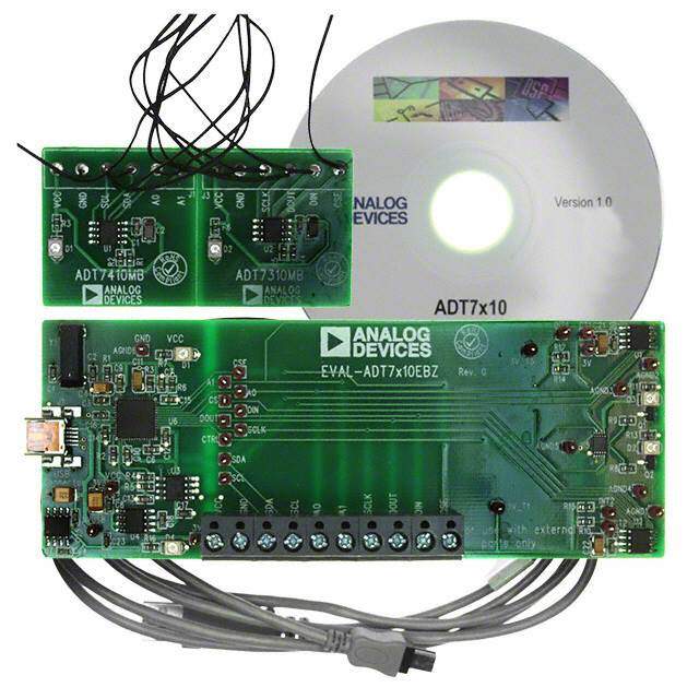
EVAL-ADT7X10EBZ产品简介:
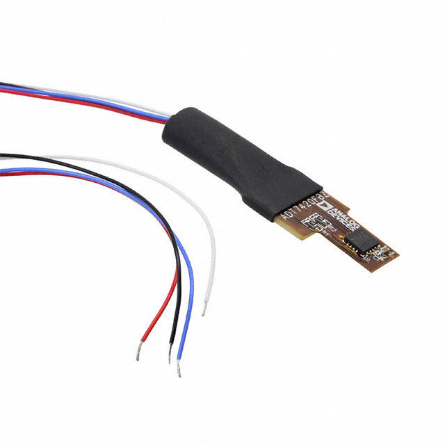
ICGOO电子元器件商城为您提供EVAL-ADT7X10EBZ由Analog设计生产,在icgoo商城现货销售,并且可以通过原厂、代理商等渠道进行代购。 EVAL-ADT7X10EBZ价格参考¥445.49-¥445.49。AnalogEVAL-ADT7X10EBZ封装/规格:评估板 - 传感器, ADT7410 - Temperature Sensor Evaluation Board。您可以下载EVAL-ADT7X10EBZ参考资料、Datasheet数据手册功能说明书,资料中有EVAL-ADT7X10EBZ 详细功能的应用电路图电压和使用方法及教程。
| 参数 | 数值 |
| 产品目录 | 编程器,开发系统半导体 |
| 描述 | BOARD EVAL FOR ADT7410温度传感器开发工具 EVAL BRD - ADT7410 |
| 产品分类 | |
| 品牌 | Analog Devices |
| 产品手册 | |
| 产品图片 |
|
| rohs | 符合RoHS无铅 / 符合限制有害物质指令(RoHS)规范要求 |
| 产品系列 | 传感器开发工具,温度传感器开发工具,Analog Devices EVAL-ADT7X10EBZ- |
| 数据手册 | |
| 产品型号 | EVAL-ADT7X10EBZ |
| 产品目录页面 | |
| 产品种类 | 温度传感器开发工具 |
| 传感器类型 | 温度 |
| 使用的IC/零件 | ADT7410 |
| 其它名称 | EVAL-ADT7410EBZ |
| 商标 | Analog Devices |
| 封装 | Bulk |
| 嵌入式 | 否 |
| 工作电源电压 | 2.7 V to 5.5 V |
| 工作电源电流 | 230 uA |
| 工具用于评估 | ADT7410 |
| 工厂包装数量 | 1 |
| 感应范围 | -55°C ~ 150°C |
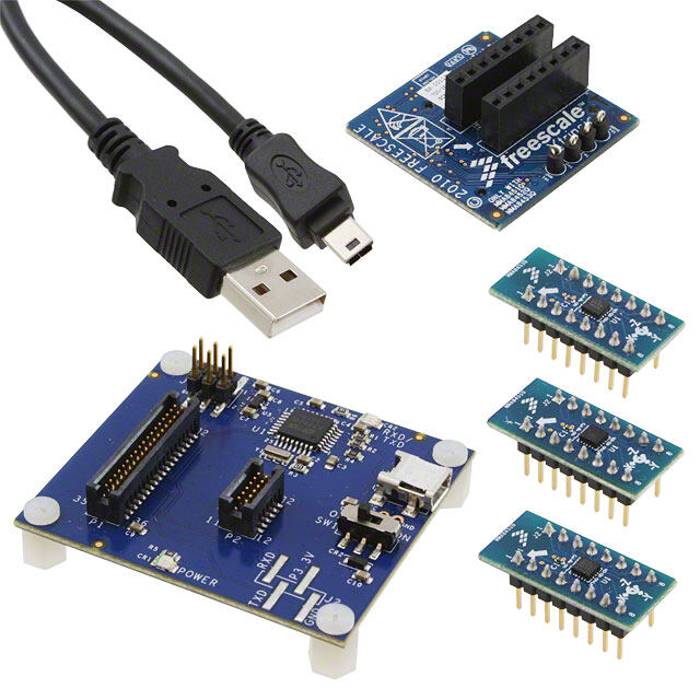
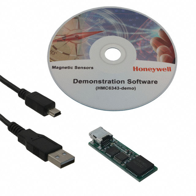
| 所含物品 | 2 板,线缆 |
| 接口 | I²C |
| 接口类型 | I2C |
| 最大工作温度 | + 150 C |
| 最小工作温度 | - 55 C |
| 标准包装 | 1 |
| 灵敏度 | ±0.5°C |
| 电压-电源 | 2.7 V ~ 5.5 V |
| 相关产品 | /product-detail/zh/ADT7410TRZ-REEL7/ADT7410TRZ-REEL7TR-ND/2056653/product-detail/zh/ADT7410TRZ-REEL/ADT7410TRZ-REELTR-ND/2056652/product-detail/zh/ADT7410TRZ/ADT7410TRZ-ND/2056175 |
| 系列 | ADT7410 |


- 商务部:美国ITC正式对集成电路等产品启动337调查
- 曝三星4nm工艺存在良率问题 高通将骁龙8 Gen1或转产台积电
- 太阳诱电将投资9.5亿元在常州建新厂生产MLCC 预计2023年完工
- 英特尔发布欧洲新工厂建设计划 深化IDM 2.0 战略
- 台积电先进制程称霸业界 有大客户加持明年业绩稳了
- 达到5530亿美元!SIA预计今年全球半导体销售额将创下新高
- 英特尔拟将自动驾驶子公司Mobileye上市 估值或超500亿美元
- 三星加码芯片和SET,合并消费电子和移动部门,撤换高东真等 CEO
- 三星电子宣布重大人事变动 还合并消费电子和移动部门
- 海关总署:前11个月进口集成电路产品价值2.52万亿元 增长14.8%

PDF Datasheet 数据手册内容提取
±0.5°C Accurate, 16-Bit Digital I2C Temperature Sensor Data Sheet ADT7410 FEATURES GENERAL DESCRIPTION High performance The ADT7410 is a high accuracy digital temperature sensor in a Temperature accuracy narrow SOIC package. It contains a band gap temperature reference ±0.5°C from −40°C to +105°C (2.7 V to 3.6 V) and a 13-bit ADC to monitor and digitize the temperature to a ±0.4°C from −40°C to +105°C (3.0 V) 0.0625°C resolution. The ADC resolution, by default, is set to 16-bit temperature resolution: 0.0078°C 13 bits (0.0625°C). This can be changed to 16 bits (0.0078°C) by Fast first temperature conversion on power-up of 6 ms setting Bit 7 in the configuration register (Register Address 0x03). Easy implementation The ADT7410 is guaranteed to operate over supply voltages from No temperature calibration/correction required by user 2.7 V to 5.5 V. Operating at 3.3 V, the average supply current is typi- No linearity correction required cally 210 μA. The ADT7410 has a shutdown mode that powers Low power down the device and offers a shutdown current of typically 2 μA. Power saving 1 sample per second (SPS) mode 700 µW typical at 3.3 V in normal mode The ADT7410 is rated for operation over the −55°C to +150°C 7 µW typical at 3.3 V in shutdown mode temperature range. Wide operating ranges Pin A0 and Pin A1 are available for address selection, giving the Temperature range: −55°C to +150°C ADT7410 four possible I2C addresses. The CT pin is an open- Voltage range: 2.7 V to 5.5 V drain output that becomes active when the temperature exceeds Programmable interrupts a programmable critical temperature limit. The default critical Critical overtemperature interrupt temperature limit is 147°C. The INT pin is also an open-drain Overtemperature/undertemperature interrupt output that becomes active when the temperature exceeds a I2C-compatible interface programmable limit. The INT and CT pins can operate in either 8-lead narrow SOIC RoHS-compliant package comparator or interrupt mode. APPLICATIONS Medical equipment Environmental control systems Computer thermal monitoring Thermal protection Industrial process control Power system monitors Hand-held applications FUNCTIONAL BLOCK DIAGRAM VDD 8 TEMPERATURE ADT7410 VALUE REGISTER INTERNAL OSCILLATOR 6 CT CONFIGURATION TCRIT REGISTER INTERNAL TCRIT REFERENCE REGISTER 5 INT RETGHIISGTHER TEMSPEENRSAOTRURE MODUΣ-LΔATOR THIGH TLOW REGISTER THYST POINTER FILTER TLOW REGISTER REGISTER LOGIC A0 3 I2C INTERFACE 1 SCL A1 4 2 SDA GN7D 06560-001 Figure 1. R ev. C Document Feedback Information furnished by Analog Devices is believed to be accurate and reliable. However, no responsibility is assumed by Analog Devices for its use, nor for any infringements of patents or other One Technology Way, P.O. Box 9106, Norwood, MA 02062-9106, U.S.A. rights of third parties that may result from its use. Specifications subject to change without notice. No license is granted by implication or otherwise under any patent or patent rights of Analog Devices. Tel: 781.329.4700 ©2009–2017 Analog Devices, Inc. All rights reserved. Trademarks and registered trademarks are the property of their respective owners. Technical Support www.analog.com
ADT7410 Data Sheet TABLE OF CONTENTS Temperature Value Registers .................................................... 13 Features .............................................................................................. 1 Applications ....................................................................................... 1 Status Register ............................................................................. 14 General Description ......................................................................... 1 Configuration Register .............................................................. 14 T Setpoint Registers ............................................................. 15 Functional Block Diagram .............................................................. 1 HIGH T Setpoint Registers .............................................................. 15 Revision History ............................................................................... 2 LOW T Setpoint Registers .............................................................. 15 Specifications ..................................................................................... 3 CRIT T Setpoint Register ............................................................... 16 I2C Timing Specifications ............................................................ 4 HYST Absolute Maximum Ratings ............................................................ 5 ID Register................................................................................... 16 ESD Caution .................................................................................. 5 Serial Interface ................................................................................ 17 Pin Configurations and Function Descriptions ........................... 6 Serial Bus Address ...................................................................... 17 Writing Data ............................................................................... 18 Typical Performance Characteristics ............................................. 7 Reading Data ............................................................................... 19 Theory of Operation ........................................................................ 9 Reset ............................................................................................. 19 Circuit Information ...................................................................... 9 General Call ................................................................................ 19 Converter Details .......................................................................... 9 Temperature Measurement ......................................................... 9 INT and CT Outputs ...................................................................... 21 One-Shot Mode .......................................................................... 10 Undertemperature and Overtemperature Detection ............ 21 Applications Information .............................................................. 23 1 SPS Mode .................................................................................. 10 Thermal Response Time ........................................................... 23 Shutdown ..................................................................................... 11 Supply Decoupling ..................................................................... 23 Fault Queue ................................................................................. 11 Temperature Monitoring ........................................................... 23 Temperature Data Format ......................................................... 12 Outline Dimensions ....................................................................... 24 Temperature Conversion Formulas ......................................... 12 Ordering Guide .......................................................................... 24 Registers ........................................................................................... 13 Address Pointer Register ........................................................... 13 REVISION HISTORY 9/2017—Rev. B to Rev. C Changes to Figure 21 ...................................................................... 22 Removed 16-Lead LFCSP ............................................. Throughout Updated Outline Dimensions ....................................................... 24 Changes to Table 3 ............................................................................ 5 Changes to Ordering Guide .......................................................... 24 Deleted Figure 5; Renumbered Sequentially ................................. 6 Changes to Table 4 ............................................................................ 6 12/2011—Rev. 0 to Rev. A Changes to Table 6 .......................................................................... 13 Changes to Features Section ............................................................ 1 Updated Outline Dimensions, Deleted Figure 24 ...................... 24 Changes to Table 1 ............................................................................. 3 Changes to Ordering Guide .......................................................... 24 Changes to Figure 5 ........................................................................... 7 Changes to One-Shot Mode Section and 1 SPS Mode 7/2016—Rev. A to Rev. B Section .............................................................................................. 10 Added 16-Lead LFCSP ....................................................... Universal Changes to Shutdown Section ...................................................... 11 Changes to Table 3 ............................................................................ 5 Changes to Table 8 and Table 9 .................................................... 13 Added Figure 5; Renumbered Sequentially .................................. 6 Changes to Table 10 and Table 11 ................................................ 14 Changes to Table 4 ............................................................................ 6 Changes to Ordering Guide .......................................................... 24 Changes to Table 9 .......................................................................... 13 Changes to Table 10 ........................................................................ 14 4/2009—Revision 0: Initial Version Changes to Interrupt Mode Section and Figure 20 .................... 21 Rev. C | Page 2 of 24
Data Sheet ADT7410 SPECIFICATIONS T = −55°C to +150°C, V = 2.7 V to 5.5 V, unless otherwise noted. A DD Table 1. Parameter Min Typ Max Unit Test Conditions/Comments TEMPERATURE SENSOR AND ADC Accuracy1 −0.05 ±0.42 °C T = −40°C to +105°C, V = 3.0 V A DD ±0.44 °C T = −40°C to +105°C, V = 2.7 V to 3.3 V A DD ±0.5 °C T = −55°C to +125°C, V = 3.0 V A DD ±0.5 °C T = −40°C to +105°C, V = 2.7 V to 3.6 V A DD ±0.7 °C T = −55°C to +150°C, V = 2.7 V to 3.6 V A DD ±0.8 °C T = −40°C to +105°C, V = 4.5 V to 5.5 V A DD ±1.0 °C T = −55°C to +150°C, V = 2.7 V to 5.5 V A DD ADC Resolution 13 Bits Twos complement temperature value of the sign bit plus 12 ADC bits (power-up default resolution) 16 Bits Twos complement temperature value of the sign bit plus 15 ADC bits (Bit 7 = 1 in the configuration register) Temperature Resolution 13-Bit 0.0625 °C 13-bit resolution (sign + 12-bit) 16-Bit 0.0078 °C 16-bit resolution (sign + 15-bit) Temperature Conversion Time 240 ms Continuous conversion and one-shot conversion modes Fast Temperature Conversion Time 6 ms First conversion on power-up only 1 SPS Conversion Time 60 ms Conversion time for 1 SPS mode Temperature Hysteresis ±0.002 °C Temperature cycle = 25°C to 125°C and back to 25°C Repeatability3 ±0.015 °C T = 25°C A DC PSRR 0.1 °C/V T = 25°C A DIGITAL OUTPUTS (OPEN DRAIN) High Output Leakage Current, I 0.1 5 µA CT and INT pins pulled up to 5.5 V OH Output High Current 1 mA V = 5.5 V OH Output Low Voltage, V 0.4 V I = 2 mA at 5.5 V, I = 1 mA at 3.3 V OL OL OL Output High Voltage, V 0.7 × V V OH DD Output Capacitance, C 3 pF OUT DIGITAL INPUTS Input Current ±1 µA V = 0 V to V IN DD Input Low Voltage, V 0.4 V IL Input High Voltage, V 0.7 × V V IH DD SCL, SDA Glitch Rejection 50 ns Input filtering suppresses noise spikes of less than 50 ns Pin Capacitance 5 10 pF POWER REQUIREMENTS Supply Voltage 2.7 5.5 V Supply Current At 3.3 V 210 250 µA Peak current while converting, I2C interface inactive At 5.5 V 250 300 µA Peak current while converting, I2C interface inactive 1 SPS Current At 3.3 V 46 µA V = 3.3 V, 1 SPS mode, T = 25°C DD A At 5.5 V 65 µA V = 5.5 V, 1 SPS mode, T = 25°C DD A Shutdown Current At 3.3 V 2.0 15 µA Supply current in shutdown mode At 5.5 V 5.2 25 µA Supply current in shutdown mode Power Dissipation Normal Mode 700 µW V = 3.3 V, normal mode at 25°C DD Power Dissipation 1 SPS 150 µW Power dissipated for V = 3.3 V, T = 25°C DD A 1 Accuracy includes lifetime drift. 2 The equivalent 3 σ limits are ±0.33°C. This 3 σ specification is provided to enable comparison with other vendors who use these limits. 3 Based on a floating average of 10 readings. Rev. C | Page 3 of 24
ADT7410 Data Sheet I2C TIMING SPECIFICATIONS T = −55°C to +150°C, V = 2.7 V to 5.5 V, unless otherwise noted. All input signals are specified with rise time (t ) = fall time (t) = 5 ns A DD R F (10% to 90% of V ) and timed from a voltage level of 1.6 V. DD Table 2. Parameter Min Typ Max Unit Test Conditions/Comments SERIAL INTERFACE1, 2 See Figure 2 SCL Frequency 0 400 kHz SCL High Pulse Width, t 0.6 µs HIGH SCL Low Pulse Width, t 1.3 µs LOW SCL, SDA Rise Time, t 0.3 µs R SCL, SDA Fall Time, t 0.3 µs F Hold Time (Start Condition), t 0.6 µs After this period, the first clock is generated HD;STA Setup Time (Start Condition), t 0.6 µs Relevant for repeated start condition SU;STA Data Setup Time, t 0.25 µs V ≥ 3.0 V SU;DAT DD 0.35 µs V < 3.0 V DD Setup Time (Stop Condition), t 0.6 µs SU;STO Data Hold Time, t (Master) 0 µs HD;DAT Bus-Free Time (Between Stop and Start Condition), t 1.3 µs BUF 1 Sample tested during initial release to ensure compliance. 2 All input signals are specified with input rise/fall times = 3 ns, measured between the 10% and 90% points. Timing reference points at 50% for inputs and outputs. Output load = 10 pF. Timing Diagram tLOW tR tF tHD:STA SCL tHD:STA tHD:DAT tHIGH tSU:DAT tSU:STA tSU:STO SDA PtBUF S S P 06560-002 Figure 2. Serial Interface Timing Diagram Rev. C | Page 4 of 24
Data Sheet ADT7410 ABSOLUTE MAXIMUM RATINGS Table 3. Stresses at or above those listed under Absolute Maximum Parameter Rating Ratings may cause permanent damage to the product. This is a V to GND −0.3 V to +7 V stress rating only; functional operation of the product at these DD SDA Voltage to GND −0.3 V to V + 0.3 V or any other conditions above those indicated in the operational DD SCL Output Voltage to GND −0.3 V to V + 0.3 V section of this specification is not implied. Operation beyond DD A0 Input Voltage to GND −0.3 V to V + 0.3 V the maximum operating conditions for extended periods may DD A1 Input Voltage to GND −0.3 V to V + 0.3 V affect product reliability. DD CT and INT Output Voltage to GND −0.3 V to V + 0.3 V DD 1.2 ESD Rating (Human Body Model) 2.0 kV Operating Temperature Range −55°C to +150°C W) 1.0 Storage Temperature Range −65°C to +160°C N ( O Maximum Junction Temperature, TJMAX 150°C TI 8-Lead SOIC-N (R-8) SIPA 0.8 S Power Dissipation1 WMAX = (TJMAX − TA2)/θJA R DI 0.6 Thermal Impedance3 E W O θJA, Junction-to-Ambient (Still Air) 121°C/W M P 0.4 θ , Junction-to-Case 56°C/W U JC M IR Reflow Soldering 220°C AXI M 0.2 Peak Temperature (RoHS-Compliant 260°C (0°C) MAX PD = 3.4mW AT 150°C Package) TRiammep a-tU Ppe Raakt Tee mperature 320°C s/esce ct om 4a0x ismecu m 0 –55–50–40–30–20–10010TE20MP30ER40AT50UR60E (70°C80) 90100110120130140150 06560-003 Ramp-Down Rate −6°C/sec maximum Figure 3. SOIC_N Maximum Power Dissipation vs. Temperature Time from 25°C to Peak Temperature 8 minutes maximum 1 Values relate to package being used on a standard 2-layer PCB. This gives a ESD CAUTION worst-case θJA and θJC. See Figure 3 for a plot of maximum power dissipation vs. ambient temperature (TA). 2 TA = ambient temperature. 3 Junction-to-case resistance is applicable to components featuring a preferential flow direction, for example, components mounted on a heat sink. Junction-to-ambient is more useful for air-cooled, PCB-mounted components. Rev. C | Page 5 of 24
ADT7410 Data Sheet PIN CONFIGURATIONS AND FUNCTION DESCRIPTIONS SCL 1 8 VDD SDA 2 ADT7410 7 GND AA01 34 (NToOt Pto V SIEcaWle) 65 CINTT 06560-005 Figure 4. Pin Configuration Table 4. Pin Function Descriptions Pin No. Mnemonic Description 1 SCL I2C Serial Clock Input. The serial clock is used to clock in and clock out data to and from any register of the ADT7410. Open-drain configuration. A pull-up resistor is required, typically 10 kΩ. 2 SDA I2C Serial Data Input/Output. Serial data to and from the part is provided on this pin. Open-drain configuration. A pull-up resistor is required, typically 10 kΩ. 3 A0 I2C Serial Bus Address Selection Pin. Logic input. Connect to GND or V to set an I2C address. DD 4 A1 I2C Serial Bus Address Selection Pin. Logic input. Connect to GND or V to set an I2C address. DD 5 INT Overtemperature and Undertemperature Indicator. Logic output. Power-up default setting is as an active low comparator interrupt. Open-drain configuration. A pull-up resistor is required, typically 10 kΩ. 6 CT Critical Overtemperature Indicator. Logic output. Power-up default polarity is active low. Open-drain configuration. A pull-up resistor is required, typically 10 kΩ. 7 GND Analog and Digital Ground. 8 V Positive Supply Voltage (2.7 V to 5.5 V). Decouple the supply with a 0.1 μF ceramic capacitor to DD ground. Rev. C | Page 6 of 24
Data Sheet ADT7410 TYPICAL PERFORMANCE CHARACTERISTICS 1.0 0.30 0.8 5.5V CONTINUOUS CONVERSION 0.25 0.6 OR (°C) 0.4 MAX ACCURACY LIMITS 0.20 3C.O0VN VCEORNSTIIONNUOUS RR 0.2 E A) URE 0 (mD0.15 AT–0.2 ID R MPE–0.4 0.10 TE MAX ACCURACY LIMITS 5.5V 1SPS –0.6 0.05 –0.8 3.0V 1SPS –1.0–60 –40 –20 0 T2E0MPE4R0ATU6R0E (°8C0) 100 120 140 160 06560-006 –0100 –50 0TEMPERA5T0URE (°C1)00 150 200 06560-007 Figure 5. Temperature Accuracy at 3 V Figure 7. Operating Supply Current vs. Temperature 1.0 30 0.8 MAX ACCURACY LIMITS 25 0.6 C) OR (° 0.4 µA) 20 RE ERR 0.20 WN I (DD 15 MPERATU––00..42 SHUTDO 10 5.5V E T 5.0V –0.6 MAX ACCURACY LIMITS 5 4.5V 3.3V –0.8 3.6V 3.0V 2.7V –1.0–60 –40 –20 0 T2E0MPE4R0ATU6R0E (°8C0) 100 120 140 160 06560-024 0–100 –50 0TEMPERA5T0URE (°C1)00 150 200 06560-025 Figure 6. Temperature Accuracy at 5 V Figure 8. Shutdown Current vs. Temperature Rev. C | Page 7 of 24
ADT7410 Data Sheet 0.30 160 0.25 IDD CONTINUOUS CONVERSION 140 120 0.20 C) E (° 100 I (mA)DD0.15 PERATUR 80 M 60 0.10 E T 40 IDD 1SPS 0.05 20 0 0 2.5 3.0 3.5SUPP4L.Y0 VOLT4A.5GE (V)5.0 5.5 6.0 06560-008 0 5 10 1T5IME (S2e0conds2)5 30 35 40 06560-011 Figure 9. Average Operating Supply Current vs. Supply Voltage at 25°C Figure 11. Response to Thermal Shock 8 7 6 A) µ (D 5 D WN I 4 O D UT 3 H S 2 1 0 2.5 3.0 3.5SUPP4L.Y0 VOLTA4.G5E (V) 5.0 5.5 6.0 06560-009 Figure 10. Shutdown Current vs. Supply Voltage at 25°C Rev. C | Page 8 of 24
Data Sheet ADT7410 THEORY OF OPERATION CIRCUIT INFORMATION TEMPERATURE MEASUREMENT The ADT7410 is a 13-bit digital temperature sensor that In normal mode, the ADT7410 runs an automatic conversion is extendable to 16 bits for greater resolution. An on-board sequence. During this automatic conversion sequence, a conversion temperature sensor generates a voltage proportional to absolute takes 240 ms to complete and the ADT7410 is continuously temperature, which is compared to an internal voltage reference converting. This means that as soon as one temperature conversion and input to a precision digital modulator. is completed, another temperature conversion begins. Each temperature conversion result is stored in the temperature value The on-board temperature sensor has excellent accuracy registers and is available through the I2C interface. In continuous and linearity over the entire rated temperature range without conversion mode, the read operation provides the most recent needing correction or calibration by the user. converted result. The sensor output is digitized by a Σ-Δ modulator, also known as On power-up, the first conversion is a fast conversion, taking the charge balance type analog-to-digital converter. This type of typically 6 ms. If the temperature exceeds 147°C, the CT pin converter uses time domain oversampling and a high accuracy asserts low. If the temperature exceeds 64°C, the INT pin asserts comparator to deliver 16 bits of resolution in an extremely low. Fast conversion temperature accuracy is typically within ±5°C. compact circuit. The conversion clock for the part is generated internally. No Configuration register functions consist of external clock is required except when reading from and Switching between 13-bit and 16-bit resolution writing to the serial port. Switching between normal operation and full power-down The measured temperature value is compared with a critical Switching between comparator and interrupt event modes temperature limit (stored in the 16-bit T setpoint read/write CRIT on the INT and CT pins register), a high temperature limit (stored in the 16-bit T set- HIGH Setting the active polarity of the CT and INT pins point read/write register), and a low temperature limit (stored in Setting the number of faults that activate CT and INT the 16-bit T setpoint read/write register). If the measured value LOW Enabling the standard one-shot mode and 1 SPS mode exceeds these limits, the INT pin is activated; and if it exceeds the CONVERTER DETAILS TCRIT limit, the CT pin is activated. The INT and CT pins are programmable for polarity via the configuration register, and the The Σ-Δ modulator consists of an input sampler, a summing INT and CT pins are also programmable for interrupt mode via network, an integrator, a comparator, and a 1-bit DAC. This the configuration register. architecture creates a negative feedback loop and minimizes the integrator output by changing the duty cycle of the comparator output in response to input voltage changes. The comparator samples the output of the integrator at a much higher rate than the input sampling frequency. This oversampling spreads the quantization noise over a much wider band than that of the input signal, improving overall noise performance and increasing accuracy. The modulated output of the comparator is encoded using a circuit technique that results in I2C temperature data. Σ-∆ MODULATOR INTEGRATOR COMPARATOR VOLTAGE REF AND VPTAT 1-BIT DAC 1-BIT GECNLEORACTKOR LPFF IDLTIGEIRTAL 13-BIT TERMEVPGAEIRLSUATETEURRE 06560-012 Figure 12. Σ-Δ Modulator Rev. C | Page 9 of 24
ADT7410 Data Sheet ONE-SHOT MODE CT and INT Operation in One-Shot Mode When one-shot mode is enabled, the ADT7410 immediately See Figure 13 for more information on one-shot CT pin completes a conversion and then goes into shutdown mode. The operation for TCRIT overtemperature events when one of the one-shot mode is useful when one of the circuit design priorities is limits is exceeded. Note that in interrupt mode, a read from to reduce power consumption. any register resets the INT and CT pins. To enable one-shot mode, set Bits[6:5] of the configuration For the INT pin in the comparator mode, if the temperature register (Register Address 0x03) to 01. drops below the THIGH − THYST value or goes above the TLOW + T value, a write to the one-shot bits (Bit 5 and Bit 6 of the After writing to the operation mode bits, wait at least 240 ms HYST configuration register, Register Address 0x03) resets the INT pin. before reading back the temperature from the temperature value register. This delay ensures that the ADT7410 has adequate time For the CT pin in the comparator mode, if the temperature to power up and complete a conversion. drops below the TCRIT − THYST value, a write to the one-shot bits (Bit 5 and Bit 6 of the configuration register, Register To obtain an updated temperature conversion, reset Bits[6:5] of the Address 0x03) resets the CT pin. See Figure 13. configuration register (Register Address 0x03) to 01. Note that when using one-shot mode, ensure that the refresh 1 SPS MODE rate is appropriate to the application being used. In this mode, the part performs one measurement per second. A conversion takes only 60 ms, and it remains in the idle state for the remaining 940 ms period. This mode is enabled by writing 1 to Bit 6 and 0 to Bit 5 of the configuration register (Register Address 0x03). TEMPERATURE 149°C 148°C 147°C TCRIT 146°C 145°C 144°C 143°C 142°C TCRIT– THYST 141°C 140°C CT PIN POLARITY =ACTIVE LOW CT PIN POLARITY =ACTIVE HIGH TIME WRITETO WRITETO WRITETO BIT 5AND BIT 6 OF BIT 5AND BIT 6 OF BIT 5AND BIT 6 OF CONFIGURATION CONFIGURATION CONFIGURATION REGISTER.* REGISTER.* REGISTER.* *THERE IS A 240ms DELAY BETWEEN WRITINGTO THE CONFIGURATION REGISTERTO START AC OSNTAVNERDSAIRODN O TNIMEE-S. HTOHET CDOELNAVYE IRSS 6IO0mNsA INND T THHEE C CATS EP IONF G AO 1IN SGPASC CTOIVNEV.E TRHSISIO INS. DUETO THE 06560-013 Figure 13. One-Shot CT Pin Rev. C | Page 10 of 24
Data Sheet ADT7410 SHUTDOWN FAULT QUEUE The ADT7410 can be placed in shutdown mode by writing 1 Bit 0 and Bit 1 of the configuration register (Register Address to Bit 6 and 1 to Bit 5 of the configuration register (Register 0x03) are used to set up a fault queue. The queue can facilitate up Address 0x03), in which case the entire IC is shut down and to four fault events to prevent false tripping of the INT and CT pins no further conversions are initiated until the ADT7410 is when the ADT7410 is used in a noisy temperature environment. taken out of shutdown mode. The ADT7410 can be taken The number of faults set in the queue must occur consecutively out of shutdown mode by writing 0 to Bit 6 and 0 to Bit 5 in the to set the INT and CT outputs. For example, if the number of configuration register (Register Address 0x03). The ADT7410 faults set in the queue is four, then four consecutive temperature typically takes 1 ms (with a 0.1 µF decoupling capacitor) to conversions must occur with each result exceeding a temperature come out of shutdown mode. The conversion result from the limit in any of the limit registers before the INT and CT pins are last conversion prior to shutdown can still be read from the activated. If two consecutive temperature conversions exceed a ADT7410 even when it is in shutdown mode. When the part is temperature limit and the third conversion does not, the fault taken out of shutdown mode, the internal clock is started and a count is reset back to zero. conversion is initiated. Rev. C | Page 11 of 24
ADT7410 Data Sheet TEMPERATURE DATA FORMAT TEMPERATURE CONVERSION FORMULAS One LSB of the ADC corresponds to 0.0625°C in 13-bit mode. 16-Bit Temperature Data Format The ADC can theoretically measure a temperature range of Positive Temperature = ADC Code (dec)/128 255°C, but the ADT7410 is guaranteed to measure a low value Negative Temperature = (ADC Code (dec) − 65,536)/128 temperature limit of −55°C to a high value temperature limit where ADC Code uses all 16 bits of the data byte, including the of +150°C. The temperature measurement result is stored in sign bit. the 16-bit temperature value register and is compared with the high temperature limits stored in the T setpoint register and Negative Temperature = (ADC Code (dec) − 32,768)/128 CRIT the THIGH setpoint register. It is also compared with the low where Bit 15 (sign bit) is removed from the ADC code. temperature limit stored in the T setpoint register. LOW 13-Bit Temperature Data Format Temperature data in the temperature value register, the TCRIT Positive Temperature = ADC Code (dec)/16 setpoint register, the T setpoint register, and the T HIGH LOW Negative Temperature = (ADC Code (dec) − 8192)/16 setpoint register are represented by a 13-bit twos complement where ADC Code uses the first 13 MSBs of the data byte, word. The MSB is the temperature sign bit. The three LSBs, Bit 0 including the sign bit. to Bit 2, on power-up, are not part of the temperature conver- sion result and are flag bits for TCRIT, THIGH, and TLOW. Table 5 Negative Temperature = (ADC Code (dec) − 4096)/16 shows the 13-bit temperature data format without Bit 0 to Bit 2. where Bit 15 (sign bit) is removed from the ADC code. The number of bits in the temperature data-word can be extended 10-Bit Temperature Data Format to 16 bits, twos complement, by setting Bit 7 to 1 in the confi- Positive Temperature = ADC Code (dec)/2 guration register (Register Address 0x03). When using a 16-bit Negative Temperature = (ADC Code (dec) − 1024)/2 temperature data value, Bit 0 to Bit 2 are not used as flag bits and are, instead, the LSB bits of the temperature value. The where ADC Code uses all 10 bits of the data byte, including the power-on default setting has a 13-bit temperature data value. sign bit. Reading back the temperature from the temperature value register Negative Temperature = (ADC Code (dec) − 512)/2 requires a 2-byte read. Designers that use a 9-bit temperature where Bit 9 (sign bit) is removed from the ADC code. data format can still use the ADT7410 by ignoring the last four 9-Bit Temperature Data Format LSBs of the 13-bit temperature value. These four LSBs are Bit 6 Positive Temperature = ADC Code (dec) to Bit 3 in Table 5. Negative Temperature = ADC Code (dec) − 512 Table 5. 13-Bit Temperature Data Format where ADC Code uses all nine bits of the data byte, including Digital Output Temperature (Binary) Bits[15:3] Digital Output (Hex) the sign bit. −55°C 1 1100 1001 0000 0x1C90 Negative Temperature = ADC Code (dec) − 256 −50°C 1 1100 1110 0000 0x1CE0 where Bit 8 (sign bit) is removed from the ADC code. −25°C 1 1110 0111 0000 0x1E70 −0.0625°C 1 1111 1111 1111 0x1FFF 0°C 0 0000 0000 0000 0x000 +0.0625°C 0 0000 0000 0001 0x001 +25°C 0 0001 1001 0000 0x190 +50°C 0 0011 0010 0000 0x320 +125°C 0 0111 1101 0000 0x7D0 +150°C 0 1001 0110 0000 0x960 Rev. C | Page 12 of 24
Data Sheet ADT7410 REGISTERS The ADT7410 contains 14 registers: ADDRESS POINTER REGISTER • Nine temperature registers This register is always the first register written to during a write • A status register to the ADT7410. It must be set to the address of the register • An ID register to which the write or read transaction is intended. Table 7 • A configuration register shows the register address of each register on the ADT7410. • An address pointer register The default value of the address pointer register is 0x00. • A software reset All registers are eight bits wide. The temperature value registers, Table 7. Address Pointer Register the status register, and the ID register are read-only. The software P7 P6 P5 P4 P3 P2 P1 P0 reset is a write-only register. On power-up, the address pointer ADD7 ADD6 ADD5 ADD4 ADD3 ADD2 ADD1 ADD0 register is loaded with 0x00 and points to the temperature value register MSB. TEMPERATURE VALUE REGISTERS Table 6. ADT7410 Registers The temperature value most significant byte (MSB) and tem- Register Power-On perature value least significant byte (LSB) registers store the Address Description Default temperature measured by the internal temperature sensor. 0x00 Temperature value most significant byte 0x00 The temperature is stored in twos complement format with 0x01 Temperature value least significant byte 0x00 the MSB being the temperature sign bit. When reading from 0x02 Status 0x00 these registers, the eight MSBs (Bit 7 to Bit 15) are read first 0x03 Configuration 0x00 from Register Address 0x00 and then the eight LSBs (Bit 0 to 0x04 T setpoint most significant byte 0x20 (64°C) HIGH Bit 7) are read from Register Address 0x01. Only the temperature 0x05 T setpoint least significant byte 0x00 (64°C) HIGH value most significant byte (Register Address 0x00) needs to be 0x06 T setpoint most significant byte 0x05 (10°C) LOW loaded into the address pointer register as the address pointer 0x07 T setpoint least significant byte 0x00 (10°C) LOW auto-increments to the temperature value least significant byte 0x08 T setpoint most significant byte 0x49 (147°C) CRIT address (Register Address 0x01). 0x09 T setpoint least significant byte 0x80 (147°C) CRIT 0x0A THYST setpoint 0x05 (5°C) Bit 0 to Bit 2 are event alarm flags for TCRIT, THIGH, and TLOW. When 0x0B ID 0xCX the ADC is configured to convert the temperature to a 16-bit 0x0C Reserved 0xXX digital value then Bit 0 to Bit 2 are no longer used as flag bits 0x0D Reserved 0xXX and are instead used as the LSB bits for the extended digital value. 0x2E Reserved 0xXX 0x2F Software reset 0xXX Table 8. Temperature Value MSB Register (Register Address 0x00) Bit Default Value Type Name Description [14:8] 0000000 R Temp Temperature value in twos complement format 15 0 R Sign Sign bit, indicates if the temperature value is negative or positive Table 9. Temperature Value LSB Register (Register Address 0x01) Bit Default Value Type Name Description 0 0 R T flag/LSB0 Flags a T event if the configuration register, Register Address 0x03[7] = 0 (13-bit resolution), LOW LOW and if comparator mode is selected through the configuration register, Register Address 0x03[4]. When the temperature value is below T , this bit it set to 1. LOW Contains the Least Significant Bit 0 of the 15-bit temperature value if the configuration register, Register Address 0x03[7] = 1 (16-bit resolution). 1 0 R T flag/LSB1 Flags a T event if the configuration register, Register Address 0x03[7] = 0 (13-bit resolution), HIGH HIGH and if comparator mode is selected through the configuration register, Register Address 0x03[4]. When the temperature value is above T , this bit it set to 1. HIGH Contains the Least Significant Bit 1 of the 15-bit temperature value if the configuration register, Register Address 0x03[7] = 1 (16-bit resolution). 2 0 R T flag/LSB2 Flags a T event if the configuration register, Register Address 0x03[7] = 0 (13-bit resolution), CRIT CRIT and if comparator mode is selected through the configuration register, Register Address 0x03[4]. When the temperature value exceeds T , this bit it set to 1. CRIT Contains the Least Significant Bit 2 of the 15-bit temperature value if the configuration register, Register Address 0x03[7] = 1 (16-bit resolution). [7:3] 00000 R Temp Temperature value in twos complement format. Rev. C | Page 13 of 24
ADT7410 Data Sheet STATUS REGISTER temperature value register. In one-shot and 1 SPS modes, the RDY bit is reset after a write to the one-shot bits. This 8-bit read-only register reflects the status of the overtempera- ture and undertemperature interrupts that can cause the CT and CONFIGURATION REGISTER INT pins to go active. It also reflects the status of a temperature This 8-bit read/write register stores various configuration modes conversion operation. The interrupt flags in this register are for the ADT7410, including shutdown, overtemperature and reset by a read operation to the status register and/or when undertemperature interrupts, one-shot, continuous conversion, the temperature value returns within the temperature limits, interrupt pins polarity, and overtemperature fault queues. including hysteresis. The RDY bit is reset after a read from the Table 10. Status Register (Register Address 0x02) Bit Default Value Type Name Description [3:0] 0000 R Unused Reads back 0. 4 0 R T Set this bit to 1 when the temperature goes below the T temperature limit, and if comparator LOW LOW mode is selected through the configuration register, Register Address 0x03[4]. The bit clears to 0 when the status register is read and/or when the temperature measured goes back above the limit set in the setpoint T + T registers. LOW HYST 5 0 R T Set this bit to 1 when the temperature goes above the T temperature limit, and if comparator HIGH HIGH mode is selected through the configuration register, Register Address 0x03[4]. The bit clears to 0 when the status register is read and/or when the temperature measured goes back below the limit set in the setpoint T − T registers. HIGH HYST 6 0 R T Set this bit to 1 when the temperature goes above the T temperature limit, and if comparator CRIT CRIT mode is selected through the configuration register, Register Address 0x03[4]. This bit clears to 0 when the status register is read and/or when the temperature measured goes back below the limit set in the setpoint T − T registers. CRIT HYST 7 1 R RDY This bit goes low when the temperature conversion result is written into the temperature value register. It is reset to 1 when the temperature value register is read. In one-shot and 1 SPS modes, this bit is reset after a write to the one-shot bits. Table 11. Configuration Register (Register Address 0x03) Bit Default Value Type Name Description [1:0] 00 R/W Fault queue These two bits set the number of undertemperature/overtemperature faults that can occur before setting the INT and CT pins. This helps to avoid false triggering due to temperature noise. 00 = 1 fault (default). 01 = 2 faults. 10 = 3 faults. 11 = 4 faults. 2 0 R/W CT pin polarity This bit selects the output polarity of the CT pin. 0 = active low. 1 = active high. 3 0 R/W INT pin polarity This bit selects the output polarity of the INT pin. 0 = active low. 1 = active high. 4 0 R/W INT/CT mode This bit selects between comparator mode and interrupt mode. 0 = interrupt mode 1 = comparator mode [6:5] 00 R/W Operation mode These two bits set the operational mode for the ADT7410. 00 = continuous conversion (default). When one conversion is finished, the ADT7410 starts another. 01 = one shot. Conversion time is typically 240 ms. 10 = 1 SPS mode. Conversion time is typically 60 ms. This operational mode reduces the average current consumption. 11 = shutdown. All circuitry except interface circuitry is powered down. 7 0 R/W Resolution This bit sets up the resolution of the ADC when converting. 0 = 13-bit resolution. Sign bit + 12 bits gives a temperature resolution of 0.0625°C. 1 = 16-bit resolution. Sign bit + 15 bits gives a temperature resolution of 0.0078°C. Rev. C | Page 14 of 24
Data Sheet ADT7410 T SETPOINT REGISTERS When reading from this register, the eight MSBs (Bit 15 to Bit 8) HIGH are read first from Register Address 0x06 and then the eight LSBs The T setpoint MSB and T setpoint LSB registers store HIGH HIGH (Bit 7 to Bit 0) are read from Register Address 0x07. Only the the overtemperature limit value. An overtemperature event Register Address 0x06 (T setpoint MSB) needs to be loaded occurs when the temperature value stored in the temperature LOW into the address pointer register as the address pointer auto- value register exceeds the value stored in this register. The INT pin increments to Register Address 0x07 (T setpoint LSB). is activated if an overtemperature event occurs. The temperature LOW is stored in twos complement format with the MSB being the The default setting for the TLOW setpoint is 10°C. temperature sign bit. T SETPOINT REGISTERS CRIT When reading from this register, the eight MSBs (Bit 15 to Bit 8) The T setpoint MSB and T setpoint LSB registers store CRIT CRIT are read first from Register Address 0x04 and then the eight the critical overtemperature limit value. A critical overtemperature LSBs (Bit 7 to Bit 0) are read from Register Address 0x05. Only event occurs when the temperature value stored in the Register Address 0x04 (T setpoint MSB) needs to be loaded HIGH temperature value register exceeds the value stored in this into the address pointer register as the address pointer auto- register. The CT pin is activated if a critical overtemperature increments to Register Address 0x05 (T setpoint LSB). HIGH event occurs. The temperature is stored in twos complement The default setting for the T setpoint is 64°C. format with the MSB being the temperature sign bit. HIGH T SETPOINT REGISTERS When reading from this register, the eight MSBs (Bit 15 to Bit 8) LOW are read first from Register Address 0x08 and then the eight The T setpoint MSB and T setpoint LSB registers store LOW LOW LSBs (Bit 7 to Bit 0) are read from Register Address 0x09. Only the undertemperature limit value. An undertemperature event the Register Address 0x08 (T setpoint MSB) needs to be occurs when the temperature value stored in the temperature CRIT loaded into the address pointer register as the address pointer value register is less than the value stored in this register. The auto-increments to Register Address 0x09 (T setpoint LSB). INT pin is activated if an undertemperature event occurs. The CRIT temperature is stored in twos complement format with the MSB The default setting for the TCRIT limit is 147°C. being the temperature sign bit. Table 12. T Setpoint MSB Register (Register Address 0x04) HIGH Bit Default Value Type Name Description [15:8] 0x20 R/W T MSB MSBs of the overtemperature limit, stored in twos complement format. HIGH Table 13. T Setpoint LSB Register (Register Address 0x05) HIGH Bit Default Value Type Name Description [7:0] 0x00 R/W T LSB LSBs of the overtemperature limit, stored in twos complement format. HIGH Table 14. T Setpoint MSB Register (Register Address 0x06) LOW Bit Default Value Type Name Description [15:8] 0x05 R/W T MSB MSBs of the undertemperature limit, stored in twos complement format. LOW Table 15. T Setpoint LSB Register (Register Address 0x07) LOW Bit Default Value Type Name Description [7:0] 0x00 R/W T LSB LSBs of the undertemperature limit, stored in twos complement format. LOW Table 16. T Setpoint MSB Register (Register Address 0x08) CRIT Bit Default Value Type Name Description [15:8] 0x49 R/W T MSB MSBs of the critical overtemperature limit, stored in twos complement format. CRIT Table 17. T Setpoint LSB Register (Register Address 0x09) CRIT Bit Default Value Type Name Description [7:0] 0x80 R/W T LSB LSBs of the critical overtemperature limit, stored in twos complement format. CRIT Rev. C | Page 15 of 24
ADT7410 Data Sheet T SETPOINT REGISTER ID REGISTER HYST This 8-bit read/write register stores the temperature hysteresis This 8-bit read-only register stores the manufacturer ID in Bit 3 value for the T , T , and T temperature limits. The to Bit 7 and the silicon revision in Bit 0 to Bit 2. HIGH LOW CRIT temperature hysteresis value is stored in straight binary format using four LSBs. Increments are possible in steps of 1°C from 0°C to 15°C. The value in this register is subtracted from the T and T values and added to the T value to implement HIGH CRIT LOW hysteresis. Table 18. T Setpoint Register (Register Address 0x0A) HYST Bit Default Value Type Name Description [3:0] 0101 R/W T Hysteresis value, from 0°C to 15°C. Stored in straight binary format. The default setting is 5°C. HYST [7:4] 0000 R/W N/A Not used. Table 19. ID Register (Register Address 0x0B) Bit Default Value Type Name Description [2:0] XXX R Revision ID Contains the silicon revision identification number [7:3] 11001 R Manufacture ID Contains the manufacturer identification number Rev. C | Page 16 of 24
Data Sheet ADT7410 SERIAL INTERFACE PULL-UP PULL-UP PULL-UP VDD VDD VDD VDD VDD 10kΩ 10kΩ 10kΩ 10kΩ ADT7410 0.1µF CT SCL INT SDA TOINTERRUPTPIN A0 ONMICROCONTROLLER A1 GND 06560-014 Figure 14. Typical I2C Interface Connection Control of the ADT7410 is carried out via the I2C-compatible 2. The peripheral with the address corresponding to the transmitted address responds by pulling the data line low serial interface. The ADT7410 is connected to this bus as a slave during the low period before the ninth clock pulse, known and is under the control of a master device. as the acknowledge bit. All other devices on the bus then Figure 14 shows a typical I2C interface connection. remain idle while the selected device waits for data to be SERIAL BUS ADDRESS read from or written to it. If the R/W bit is a 0, the master Like all I2C-compatible devices, the ADT7410 has a 7-bit serial writes to the slave device. If the R/W bit is a 1, the master address. The five MSBs of this address for the ADT7410 are set reads from the slave device. to 10010. Pin A1 and Pin A0 set the two LSBs. These pins can 3. Data is sent over the serial bus in sequences of nine clock be configured two ways, low and high, to give four different pulses, eight bits of data followed by an acknowledge bit address options. Table 20 shows the different bus address options from the receiver of data. Transitions on the data line must available. The recommended pull-up resistor value on the SDA occur during the low period of the clock signal and remain and SCL lines is 10 kΩ. stable during the high period as a low-to-high transition when the clock is high, which can be interpreted as a stop signal. Table 20. I2C Bus Address Options 4. When all data bytes have been read or written, stop conditions Binary are established. In write mode, the master pulls the data A6 A5 A4 A3 A2 A1 A0 Hex line high during the 10th clock pulse to assert a stop 1 0 0 1 0 0 0 0x48 condition. In read mode, the master device pulls the data 1 0 0 1 0 0 1 0x49 line high during the low period before the ninth clock 1 0 0 1 0 1 0 0x4A pulse. This is known as a no acknowledge. The master 1 0 0 1 0 1 1 0x4B takes the data line low during the low period before the 10th clock pulse, then high during the 10th clock pulse to The serial bus protocol operates as follows: assert a stop condition. 1. The master initiates data transfer by establishing a start It is not possible to mix read and write in one operation because condition, defined as a high-to-low transition on the serial the type of operation is determined at the beginning and cannot data line, SDA, while the serial clock line, SCL, remains subsequently be changed without starting a new operation. high. This indicates that an address/data stream is going to follow. All slave peripherals connected to the serial bus respond to the start condition and shift in the next eight bits, consisting of a 7-bit address (MSB first) plus a read/ write (R/W) bit. The R/W bit determines whether data is written to, or read from, the slave device. Rev. C | Page 17 of 24
ADT7410 Data Sheet WRITING DATA registers in the same write transaction. Writing two bytes of data to these registers requires the serial bus address, the data It is possible to write either a single byte of data or two bytes to register address of the MSB register written to the address the ADT7410, depending on which registers are to be written. pointer register, followed by the two data bytes written to the Writing a single byte of data requires the serial bus address, the selected data register. This is shown in Figure 16. data register address written to the address pointer register, If more than the required number of data bytes is written to a followed by the data byte written to the selected data register. register, the register ignores these extra data bytes. To write to This is shown in Figure 15. a different register, a start or repeated start is required. For the T setpoint, T setpoint, and T setpoint HIGH LOW CRIT registers, it is possible to write to both the MSB and the LSB 1 9 1 9 SCL SDA 1 0 0 1 0 A1 A0 R/W P7 P6 P5 P4 P3 P2 P1 P0 START BY ACK. BY ACK. BY MASTER ADT7410 ADT7410 FRAME 1 FRAME 2 SERIAL BUSADDRESS BYTE ADDRESS POINTER REGISTER BYTE 1 9 SCL (CONTINUED) SDA (CONTINUED) D7 D6 D5 D4 D3 D2 D1 D0 ACK. BY STOP BY ADT7410 MASTER DFARTAA MBEY T3E 06560-016 Figure 15. Writing to a Register Followed by a Single Byte of Data 1 9 1 9 SCL SDA 1 0 0 1 0 A1 A0 R/W P7 P6 P5 P4 P3 P2 P1 P0 START BY ACK. BY ACK. BY MASTER ADT7410 ADT7410 FRAME 1 FRAME 2 SERIAL BUSADDRESS BYTE ADDRESS POINTER REGISTER BYTE 1 9 1 9 SCL (CONTINUED) SDA (CONTINUED) D15 D14 D13 D12 D11 D10 D9 D8 D7 D6 D5 D4 D3 D2 D1 D0 ACK. BY ACK. BY STOP BY ADT7410 ADT7410 MASTER DFARTAA MBEY T3E DFARTAA MBEY T4E 06560-017 Figure 16. Writing to a Register Followed by Two Bytes of Data Rev. C | Page 18 of 24
Data Sheet ADT7410 READING DATA RESET Reading data from the ADT7410 is done in a single data byte To reset the ADT7410 without having to reset the entire I2C bus, operation for the configuration register, the status register, an explicit reset command is provided. This uses a particular the T register, and the ID register. A two data byte read address pointer word as a command word to reset the part and HYST operation is needed for the temperature value register, T upload all default settings. The ADT7410 does not respond to HIGH setpoint register, T setpoint register, and the T setpoint the I2C bus commands (do not acknowledge) during the default LOW CRIT register. Reading back the contents of an 8-bit register similar values upload for approximately 200 µs. to the configuration register is shown in Figure 17. Reading The reset command address word is 0x2F. back the contents of the temperature value register is shown GENERAL CALL in Figure 18. When a master issues a slave address consisting of seven 0s with Reading back from any register first requires a single-byte write the eighth bit (R/W bit) set to 0, this is known as the general call operation to the address pointer register to set up the address of the register that is going to be read from. In the case of reading address. The general call address is for addressing every device back from the 2-byte registers, the address pointer automatically connected to the I2C bus. The ADT7410 acknowledges this increments from the MSB register address to the LSB register address and reads in the following data byte. address. If the second byte is 0x06, the ADT7410 is reset, completely To read from another register, execute another write to the uploading all default values. The ADT7410 does not respond address pointer register to set up the relevant register address. to the I2C bus commands (do not acknowledge) while the Thus, block reads are not possible, that is, there is no I2C address default values upload for approximately 200 µs. pointer auto-increment except when reading back from a 16-bit The ADT7410 does not acknowledge any other general call register. If the address pointer register has previously been set commands. up with the address of the register that is going to receive a read command, there is no need to repeat a write operation to set up the register address again. 1 9 1 9 SCL SDA 1 0 0 1 0 A1 A0 R/W P7 P6 P5 P4 P3 P2 P1 P0 START BY ACK. BY ACK. BY MASTER ADT7410 ADT7410 FRAME 1 FRAME 2 SERIAL BUSADDRESS ADDRESS POINTER REGISTER BYTE BYTE 1 9 1 9 SCL SDA 1 0 0 1 0 A2 A0 R/W D7 D6 D5 D4 D3 D2 D1 D0 REPEAT START ACK. BY NOACK. BY STOP BY BY MASTER ADT7410 MASTER MASTER FRAME 3 FRAME 4 SERIAL BBUYSTEADDRESS DATA BYTE FRREOGMIS CTOENRFIGURATION 06560-018 Figure 17. Reading Back Data from the Configuration Register Rev. C | Page 19 of 24
ADT7410 Data Sheet 1 9 1 9 SCL SDA 1 0 0 1 0 A1 A0 R/W A7 A6 A1 A0 START ADT7410 DEVICEADDRESS ACK. BY REGISTERADDRESS[A7:A0] ACK. BY ADT7410 ADT7410 SR 1 9 1 9 SCL SDA 1 0 A1 A0 R/W D7 D6 D1 D0 D7 D6 D1 D0 REPEAT ADT7410 DEVICEADDRESS ACK. BY TEMPERATURE REGISTER ACK. BY TEMPERATURE REGISTER NO START ADT7410 MSB DATA MASTER LSB DATA ACK. BY MASTER NOTES 1. A START CONDITION AT THE BEGINNING IS DEFINED AS A HIGH-TO-LOW TRANSITION ON SDA WHILE SCLK REMAINS HIGH. 2. A STOP CONDITION AT THE END IS DEFINED AS A LOW-TO-HIGH TRANSITION ON SDA WHILE SCLK REMAINS HIGH. 345... TTTHEHMEE PMRE/AWRSA TBTEIUTR RI SGE ESRNEEETGR TISAOTT EAERS1 TMTOHS EBIN NDDOAIC TAAACT KAENN AOD R WTEELAMEDDPBGEAREC AAKTT UO TRPHEEE RR EAENTGDIOIS ONTF.E RT HLES BR EDAADTBAA ACRKE T AOL WSIAGYNSA LS ETPHAARTA ITT EDDO BEYS AN OLTO WW AANCTK A BDITD.ITIONAL DATA. 06560-023 Figure 18. Reading Back Data from the Temperature Value Register Rev. C | Page 20 of 24
Data Sheet ADT7410 INT AND CT OUTPUTS Comparator Mode The INT and CT pins are open-drain outputs, and both pins require a 10 kΩ pull-up resistor to V . In comparator mode, the INT pin returns to its inactive status DD when the temperature drops below the T − T limit or UNDERTEMPERATURE AND OVERTEMPERATURE HIGH HYST rises above the T + T limit. DETECTION LOW HYST Putting the ADT7410 into shutdown mode does not reset the The INT and CT pins have two undertemperature/ INT state in comparator mode. overtemperature modes: comparator mode and interrupt mode. Interrupt Mode The interrupt mode is the default power-up overtemperature mode. The INT output pin becomes active when the temperature In interrupt mode, the INT pin only goes inactive when the is greater than the temperature stored in the THIGH setpoint register ADT7410 register is read, that is, independently, when the or less than the temperature stored in the TLOW setpoint register. temperature has recovered and gotten back to within the limits How this pin reacts after this event depends on the overtemper- before Point C, as shown in Figure 20. when the INT pin is ature mode selected. reset, it only goes active again when the temperature goes from Figure 19 illustrates the comparator and interrupt modes for an overtemperature/undertemperature condition back to events exceeding the T limit with both pin polarity settings. a temperature within the limits or vice versa. HIGH Figure 20 illustrates the comparator and interrupt modes for As shown in Figure 19, the INT pin goes active when the events exceeding the TLOW limit with both pin polarity settings. temperature rises beyond the THIGH limit and resets the next time any register is read. When reset, it does not go active again until temperatures decrease back to below T − T (Point A), HIGH HYST and when reset, it goes active again when the T /T is HIGH LOW exceeded (Point B). TEMPERATURE 82°C 81°C B 80°C THIGH 79°C 78°C 77°C 76°C 75°C A THIGH –THYST 74°C 73°C INT PIN (COMPARATOR MODE) POLARITY =ACTIVE LOW INT PIN (INTERRUPT MODE) POLARITY =ACTIVE LOW INT PIN (COMPARATOR MODE) POLARITY =ACTIVE HIGH INT PIN (INTERRUPT MODE) POLARITY =ACTIVE HIGH READ READ READ TIME 06560-020 Figure 19. INT Output Temperature Response Diagram for THIGH Overtemperature Events Rev. C | Page 21 of 24
ADT7410 Data Sheet TEMPERATURE –13°C –14°C –15°C TLOW +THYST –16°C –17°C –18°C –19°C –20°C C TLOW –21°C –22°C INT PIN (COMPARATOR MODE) POLARITY =ACTIVE LOW INT PIN (INTERRUPT MODE) POLARITY =ACTIVE LOW INT PIN (COMPARATOR MODE) POLARITY =ACTIVE HIGH INT PIN (INTERRUPT MODE) POLARITY =ACTIVE HIGH READ READ READ TIME 06560-021 Figure 20. INT Output Temperature Response Diagram for TLOW Undertemperature Events Rev. C | Page 22 of 24
Data Sheet ADT7410 APPLICATIONS INFORMATION THERMAL RESPONSE TIME TEMPERATURE MONITORING The time required for a temperature sensor to settle to a specified The ADT7410 is ideal for monitoring the thermal environment accuracy is a function of the thermal mass of the sensor and within electronic equipment. For example, the surface-mounted the thermal conductivity between the sensor and the object package accurately reflects the exact thermal conditions that being sensed. Thermal mass is often considered equivalent to affect nearby integrated circuits. capacitance. Thermal conductivity is commonly specified using The ADT7410 measures and converts the temperature at the the symbol, Q, and can be thought of as thermal resistance. It surface of its own semiconductor chip. When the ADT7410 is is commonly specified in units of degrees per watt of power used to measure the temperature of a nearby heat source, the transferred across the thermal joint. The time required for thermal impedance between the heat source and the ADT7410 the part to settle to the desired accuracy is dependent on the must be considered. thermal contact established in a particular application and the equivalent power of the heat source. In most applications, it is When the thermal impedance is determined, the temperature best to determine the settling time empirically. of the heat source can be inferred from the ADT7410 output. As SUPPLY DECOUPLING much as 60% of the heat transferred from the heat source to the thermal sensor on the ADT7410 die is discharged via the copper Decouple the ADT7410 with a 0.1 µF ceramic capacitor between tracks, the package pins, and the bond pads. Of the pins on the V and GND. This is particularly important when the ADT7410 DD ADT7410, the GND pin transfers most of the heat. Therefore, to is mounted remotely from the power supply. Precision analog measure the temperature of a heat source, it is recommended products, such as the ADT7410, require a well-filtered power that the thermal resistance between the GND pin of the ADT7410 source. Because the ADT7410 operates from a single supply, it and the GND of the heat source be reduced as much as possible. might seem convenient to tap into the digital logic power supply. Unfortunately, the logic supply is often a switch-mode design, which generates noise in the 20 kHz to 1 MHz range. In addition, fast logic gates can generate glitches hundreds of millivolts in amplitude due to wiring resistance and inductance. If possible, the power ADT7410 directly from the system power supply. This arrangement, shown in Figure 21, isolates the analog section from the logic switching transients. Even if a separate power supply trace is not available, generous supply bypassing reduces supply-line induced errors. Local supply bypassing consisting of a 0.1 µF ceramic capacitor is critical for the temperature accuracy specifications to be achieved. This decoupling capacitor must be placed as close as possible to the V pin of the ADT7410. DD TTL/CMOS LOGIC CIRCUITS 0.1µF ADT7410 SPUOPWPELRY 06560-022 Figure 21. Use of Separate Traces to Reduce Power Supply Noise Rev. C | Page 23 of 24
ADT7410 Data Sheet OUTLINE DIMENSIONS 5.00(0.1968) 4.80(0.1890) 8 5 4.00(0.1574) 6.20(0.2441) 3.80(0.1497) 1 4 5.80(0.2284) 1.27(0.0500) 0.50(0.0196) BSC 1.75(0.0688) 0.25(0.0099) 45° 0.25(0.0098) 1.35(0.0532) 8° 0.10(0.0040) 0° COPLANARITY 0.51(0.0201) 0.10 SEATING 0.31(0.0122) 0.25(0.0098) 10..2470((00..00510507)) PLANE 0.17(0.0067) COMPLIANTTOJEDECSTANDARDSMS-012-AA C(RINEOFNPEATRRREOENNLCLTEIHNEOGSNDELISYM)AEANNRDSEIAORRNOESUNANORDETEDAIN-POMPFRIFLOLMPIMIRLELIATIMTEEERTFSEO;RIRNECUQHSUEDIVIINMAELDENENSSTIIOGSNNFS.OR 012407-A Figure 22. 8-Lead Standard Small Outline Package [SOIC_N] Narrow Body (R-8) Dimensions shown in millimeters and (inches) ORDERING GUIDE Model1 Temperature Range Temperature Accuracy2 Package Description Package Option ADT7410TRZ −55°C to +150°C ±0.5°C 8-Lead Standard Small Outline Package [SOIC_N] R-8 ADT7410TRZ-REEL −55°C to +150°C ±0.5°C 8-Lead Standard Small Outline Package [SOIC_N] R-8 ADT7410TRZ-REEL7 −55°C to +150°C ±0.5°C 8-Lead Standard Small Outline Package [SOIC_N] R-8 EVAL-ADT7X10EBZ Evaluation Board 1 Z = RoHS Compliant Part. 2 Maximum accuracy over the −40°C to +105°C temperature range. I2C refers to a communications protocol originally developed by Philips Semiconductors (now NXP Semiconductors). ©2009–2017 Analog Devices, Inc. All rights reserved. Trademarks and registered trademarks are the property of their respective owners. D06560-0-9/17(C) Rev. C | Page 24 of 24
Mouser Electronics Authorized Distributor Click to View Pricing, Inventory, Delivery & Lifecycle Information: A nalog Devices Inc.: EVAL-ADT7X10EBZ ADT7410TRZ-REEL7 ADT7410TRZ-REEL ADT7410TRZ