ICGOO在线商城 > 开发板,套件,编程器 > 评估和演示板和套件 > EVAL-ADG2128EBZ

 Datasheet下载
- 型号: EVAL-ADG2128EBZ
- 制造商: Analog
- 库位|库存: xxxx|xxxx
- 要求:
| 数量阶梯 | 香港交货 | 国内含税 |
| +xxxx | $xxxx | ¥xxxx |
查看当月历史价格
查看今年历史价格
EVAL-ADG2128EBZ产品简介:
ICGOO电子元器件商城为您提供EVAL-ADG2128EBZ由Analog设计生产,在icgoo商城现货销售,并且可以通过原厂、代理商等渠道进行代购。 EVAL-ADG2128EBZ价格参考。AnalogEVAL-ADG2128EBZ封装/规格:评估和演示板和套件, ADG2128 交叉点开关/多路复用器 接口 Evaluation Board。您可以下载EVAL-ADG2128EBZ参考资料、Datasheet数据手册功能说明书,资料中有EVAL-ADG2128EBZ 详细功能的应用电路图电压和使用方法及教程。
| 参数 | 数值 |
| 产品目录 | 编程器,开发系统 |
| 描述 | BOARD EVAL FOR ADG2128 |
| 产品分类 | |
| 品牌 | Analog Devices Inc |
| 数据手册 | |
| 产品图片 |
|
| 产品型号 | EVAL-ADG2128EBZ |
| PCN设计/规格 | |
| rohs | 无铅 / 符合限制有害物质指令(RoHS)规范要求 |
| 产品系列 | - |
| 主要属性 | 8 x 12 模拟多路复用器,8 ~ 12V 或 +/- 5V |
| 主要用途 | 接口,交叉点开关/多路复用器 |
| 使用的IC/零件 | ADG2128 |
| 其它名称 | EVALADG2128EBZ |
| 嵌入式 | 否 |
| 所含物品 | 板 |
| 标准包装 | 1 |
| 相关产品 | /product-detail/zh/ADG2128BCPZ-REEL7/ADG2128BCPZ-REEL7TR-ND/1218200/product-detail/zh/ADG2128BCPZ-REEL/ADG2128BCPZ-REEL-ND/1218199/product-detail/zh/ADG2128YCPZ-HS-RL7/ADG2128YCPZ-HS-RL7DKR-ND/1120095/product-detail/zh/ADG2128BCPZ-HS-RL7/ADG2128BCPZ-HS-RL7DKR-ND/1120094/product-detail/zh/ADG2128YCPZ-HS-RL7/ADG2128YCPZ-HS-RL7CT-ND/1120075/product-detail/zh/ADG2128BCPZ-HS-RL7/ADG2128BCPZ-HS-RL7CT-ND/1120074/product-detail/zh/ADG2128YCPZ-HS-RL7/ADG2128YCPZ-HS-RL7TR-ND/1120011/product-detail/zh/ADG2128BCPZ-HS-RL7/ADG2128BCPZ-HS-RL7TR-ND/1120010/product-detail/zh/ADG2128YCPZ-REEL7/ADG2128YCPZ-REEL7TR-ND/1040672/product-detail/zh/ADG2128YCPZ-REEL/ADG2128YCPZ-REEL-ND/1040671 |
| 辅助属性 | 图形用户界面 |


- 商务部:美国ITC正式对集成电路等产品启动337调查
- 曝三星4nm工艺存在良率问题 高通将骁龙8 Gen1或转产台积电
- 太阳诱电将投资9.5亿元在常州建新厂生产MLCC 预计2023年完工
- 英特尔发布欧洲新工厂建设计划 深化IDM 2.0 战略
- 台积电先进制程称霸业界 有大客户加持明年业绩稳了
- 达到5530亿美元!SIA预计今年全球半导体销售额将创下新高
- 英特尔拟将自动驾驶子公司Mobileye上市 估值或超500亿美元
- 三星加码芯片和SET,合并消费电子和移动部门,撤换高东真等 CEO
- 三星电子宣布重大人事变动 还合并消费电子和移动部门
- 海关总署:前11个月进口集成电路产品价值2.52万亿元 增长14.8%


PDF Datasheet 数据手册内容提取
I2C® CMOS 8 × 12 Unbuffered Analog Switch Array With Dual/Single Supplies Data Sheet ADG2128 FEATURES GENERAL DESCRIPTION I2C-compatible interface 3.4 MHz high speed I2C option The ADG2128 is an analog cross point switch with an 32-lead LFCSP_VQ (5 mm × 5 mm) array size of 8 × 12. The switch array is arranged so that Double-buffered input logic there are eight columns by 12 rows, for a total of 96 switch Simultaneous update of multiple switches channels. The array is bidirectional, and the rows and columns Up to 300 MHz bandwidth can be configured as either inputs or outputs. Each of the 96 Fully specified at dual ±5 V/single +12 V operation switches can be addressed and configured through the I2C- On resistance 35 Ω maximum compatible interface. Standard, full speed, and high speed Low quiescent current < 20 µA (3.4 MHz) I2C interfaces are supported. Any simultaneous Qualified for automotive applications switch combination is allowed. An additional feature of the ADG2128 is that switches can be updated simultaneously, APPLICATIONS using the LDSW command. In addition, a RESET option AV switching in TV allows all of the switch channels to be reset/off. At power-on, Automotive infotainment all switches are in the off condition. The device is packaged AV receivers in a 32-lead, 5 mm × 5 mm LFCSP_VQ. CCTV Ultrasound applications KVM switching Telecom applications Test equipment/instrumentation PBX systems FUNCTIONAL BLOCK DIAGRAM VDD VSS VL ADG2128 1 1 SCL INPUT REGISTER SDA AND LATCHES 8 × 12 SWITCH ARRAY X0 TO X11 (I/O) 7 TO 96 DECODER 96 96 LDSW LDSW A2 A1 A0 GND Y0 TO Y7 (I/O) 05464-001 Figure 1. Rev. D Document Feedback Information furnished by Analog Devices is believed to be accurate and reliable. However, no responsibility is assumed by Analog Devices for its use, nor for any infringements of patents or other One Technology Way, P.O. Box 9106, Norwood, MA 02062-9106, U.S.A. rights of third parties that may result from its use. Specifications subject to change without notice. No license is granted by implication or otherwise under any patent or patent rights of Analog Devices. Tel: 781.329.4700 ©2006–2012 Analog Devices, Inc. All rights reserved. Trademarks and registered trademarks are the property of their respective owners. Technical Support www.analog.com
ADG2128 Data Sheet TABLE OF CONTENTS Features .............................................................................................. 1 Load Switch (LDSW) ................................................................. 18 Applications ....................................................................................... 1 Readback ..................................................................................... 18 General Description ......................................................................... 1 Serial Interface ................................................................................ 19 Functional Block Diagram .............................................................. 1 High Speed I2C Interface ........................................................... 19 Revision History ............................................................................... 2 Serial Bus Address ...................................................................... 19 Specifications ..................................................................................... 3 Writing to the ADG2128 ............................................................... 20 I2C Timing Specifications ............................................................ 7 Input Shift Register .................................................................... 20 Timing Diagram ........................................................................... 8 Write Operation.......................................................................... 22 Absolute Maximum Ratings ............................................................ 9 Read Operation........................................................................... 22 ESD Caution .................................................................................. 9 Evaluation Board ............................................................................ 24 Pin Configuration and Function Descriptions ........................... 10 Using the ADG2128 Evaluation Board ................................... 24 Typical Performance Characteristics ........................................... 11 Power Supply ............................................................................... 24 Test Circuits ..................................................................................... 15 Schematics ................................................................................... 25 Terminology .................................................................................... 17 Outline Dimensions ....................................................................... 27 Theory of Operation ...................................................................... 18 Ordering Guide .......................................................................... 27 RESET/Power-On Reset ............................................................ 18 Automotive Products ................................................................. 27 REVISION HISTORY 10/12—Rev. C to Rev. D 5/06—Rev. 0 to Rev. A Changes to Ordering Guide .......................................................... 27 Added I2C Information ...................................................... Universal Changes to Table 1 ............................................................................. 3 8/12—Rev. B to Rev. C Changes to Table 2 ............................................................................. 5 Updated Outline Dimensions (Changed CP-32-1 to CP-32-7) ...... 27 Changes to Table 4 ............................................................................. 9 Changes to Ordering Guide .......................................................... 27 Changes to Figure 24 ...................................................................... 14 Changes to Terminology Section ................................................. 17 11/11—Rev. A to Rev. B Changes to Figure 35 ...................................................................... 23 Changes to Features Section ........................................................... 1 Changes to the Ordering Guide ................................................... 27 Changes to Schematics Section .................................................... 25 Updated Outline Dimensions ....................................................... 27 1/06—Revision 0: Initial Version Changes to the Ordering Guide .................................................... 27 Added Automotive Products Section........................................... 27 Rev. D | Page 2 of 28
Data Sheet ADG2128 SPECIFICATIONS V = 12 V ± 10%, V = 0 V, V = 5 V, GND = 0 V, all specifications T to T unless otherwise noted.1 DD SS L MIN MAX, Table 1. B Version Y Version −40°C to −40°C to Parameter +25°C +85°C +25°C +125°C Unit Conditions ANALOG SWITCH Analog Signal Range V − 2 V V − 2 V V max DD DD On Resistance, R 30 30 Ω typ V = +10.8 V, V = 0 V, I = −10 mA ON DD IN S 35 40 35 42 Ω max 32 32 Ω typ V = +10.8 V, V = +1.4 V, I = −10 mA DD IN S 37 42 37 47 Ω max 45 45 Ω typ V = +10.8 V, V = +5.4 V, I = −10 mA DD IN S 50 57 50 62 Ω max On Resistance Matching 4.5 4.5 Ω typ V = +10.8 V, V = 0 V, I = −10 mA DD IN S Between Channels, ∆R 8 9 8 10 Ω max ON On Resistance Flatness, R 2.3 2.3 Ω typ V = 10.8 V, V = 0 V to +1.4 V, I = −10 mA FLAT(ON) DD IN S 3.5 4 3.5 5 Ω max 14.5 14.5 Ω typ V = 10.8 V, V = 0 V to +5.4 V, I = −10 mA DD IN S 18 20 18 22 Ω max LEAKAGE CURRENTS V = 13.2 V DD Channel Off Leakage, I ±0.03 ±0.03 µA typ V = 7 V/1 V, V = 1 V/7 V OFF X Y Channel On Leakage, I ±0.03 ±0.03 µA typ V = V = 1 V or 7 V ON X Y DYNAMIC CHARACTERISTICS2 C 11 11 pF typ OFF C 18.5 18.5 pF typ ON t 170 170 ns typ R = 300 Ω, C = 35 pF ON L L 185 190 185 195 ns max t 210 210 ns typ R = 300 Ω, C = 35 pF OFF L L 250 255 250 260 ns max THD + N 0.04 0.04 % typ R = 10 kΩ, f = 20 Hz to 20 kHz, L V = 1 V p-p S PSRR 90 dB typ f = 20 kHz; without decoupling; see Figure 24 −3 dB Bandwidth 210 210 MHz typ Individual inputs to outputs 16.5 16.5 MHz typ 8 inputs to 1 output Off Isolation −69 −69 dB typ R = 75 Ω, C = 5 pF, f = 5 MHz L L Channel-to-Channel Crosstalk R = 75 Ω, C = 5 pF, f = 5 MHz L L Adjacent Channels −63 −63 dB typ Nonadjacent Channels −76 −76 dB typ Differential Gain 0.4 0.4 % typ R = 75 Ω, C = 5 pF, f = 5 MHz L L Differential Phase 0.6 0.6 ° typ R = 75 Ω, C = 5 pF, f = 5 MHz L L Charge Injection −3.5 −3.5 pC typ V = 4 V, R = 0 Ω, C = 1 nF S S L LOGIC INPUTS (Ax, RESET)2 Input High Voltage, V 2.0 2.0 V min INH Input Low Voltage, V 0.8 0.8 V max INL Input Leakage Current, I 0.005 0.005 µA typ IN ±1 ±1 µA max Input Capacitance, C 7 7 pF typ IN Rev. D | Page 3 of 28
ADG2128 Data Sheet B Version Y Version −40°C to −40°C to Parameter +25°C +85°C +25°C +125°C Unit Conditions LOGIC INPUTS (SCL, SDA)2 Input High Voltage, V 0.7 V 0.7 V V min INH L L V + 0.3 V + 0.3 V max L L Input Low Voltage, V −0.3 −0.3 V min INL 0.3 V 0.3 V V max L L Input Leakage Current, I 0.005 0.005 µA typ V = 0 V to V IN IN L ±1 ±1 µA max Input Hysteresis 0.05 V 0.05 V V min L L Input Capacitance, C 7 7 pF typ IN LOGIC OUTPUT (SDA)2 Output Low Voltage, V 0.4 0.4 V max I = 3 mA OL SINK 0.6 0.6 V max I = 6 mA SINK Floating State Leakage Current ±1 ±1 µA max POWER REQUIREMENTS I 0.05 0.05 µA typ Digital inputs = 0 V or V DD L 1 1 µA max I 0.05 0.05 µA typ Digital inputs = 0 V or V SS L 1 1 µA max I Digital inputs = 0 V or V L L Interface Inactive 0.3 0.3 µA typ 2 2 µA max Interface Active: 400 kHz f 0.1 0.1 mA typ SCL 0.2 0.2 mA max Interface Active: 3.4 MHz f 0.4 0.4 mA typ -HS model only SCL 1.2 1.7 mA max 1 Temperature range is as follows: B version: −40°C to +85°C; Y version: −40°C to +125°C. 2 Guaranteed by design, not subject to production test. Rev. D | Page 4 of 28
Data Sheet ADG2128 V = +5 V ± 10%, V = −5 V ± 10%, V = 5 V, GND = 0 V, all specifications T to T , unless otherwise noted.1 DD SS L MIN MAX Table 2. B Version Y Version −40°C to −40°C to Parameter +25°C +125°C +25°C +125°C Unit Conditions ANALOG SWITCH Analog Signal Range V − 2 V V max DD On Resistance, R 34 34 Ω typ V = +4.5 V, V = −4.5 V, V = V , I = −10 mA ON DD SS IN SS S 40 45 40 50 Ω max 50 50 Ω typ V = +4.5 V, V = −4.5 V, V = 0 V, I = −10 mA DD SS IN S 55 65 55 70 Ω max 66 66 Ω typ V = +4.5 V, V = −4.5 V, V = +1.4 V, I = −10 mA DD SS IN S 75 85 75 95 Ω max On Resistance Matching 4.5 4.5 Ω typ V = +4.5 V, V = −4.5 V, V = V , I = −10 mA DD SS IN SS S Between Channels, ∆R 8 9 8 10 Ω max ON On Resistance Flatness, R 17 17 Ω typ V = +4.5 V, V = −4.5 V, V = V to 0 V, I = −10 mA FLAT(ON) DD SS IN SS S 20 23 20 25 Ω max 34 34 Ω typ V = +4.5 V, V = −4.5 V, V = V to +1.4 V, I = −10 mA DD SS IN SS S 42 45 42 48 Ω max LEAKAGE CURRENTS V = 5.5 V, V = 5.5 V DD SS Channel Off Leakage, I ±0.03 ±0.03 µA typ V = +4.5 V/−2 V, V = −2 V/+4.5 V OFF X Y Channel On Leakage, I ±0.03 ±0.03 µA typ V = V = −2 V or +4.5 V ON X Y DYNAMIC CHARACTERISTICS2 C 6 6 pF typ OFF C 9.5 9.5 pF typ ON t 170 170 ns typ R = 300 Ω, C = 35 pF ON L L 200 215 200 220 ns max t 210 210 ns typ R = 300 Ω, C = 35 pF OFF L L 250 255 250 260 ns max THD + N 0.04 0.04 % typ R = 10 kΩ, f = 20 Hz to 20 kHz, V = 1 V p-p L S PSRR 90 dB typ f = 20 kHz; without decoupling; see Figure 24 −3 dB Bandwidth 300 300 MHz typ Individual inputs to outputs 18 18 MHz typ 8 inputs to 1 output Off Isolation −66 −64 dB typ R = 75 Ω, C = 5 pF, f = 5 MHz L L Channel-to-Channel Crosstalk R = 75 Ω, C = 5 pF, f = 5 MHz L L Adjacent Channels −62 −62 dB typ Nonadjacent Channels −79 −79 dB typ Differential Gain 1.5 1.5 % typ R = 75 Ω, C = 5 pF, f = 5 MHz L L Differential Phase 1.8 1.8 ° typ R = 75 Ω, C = 5 pF, f = 5 MHz L L Charge Injection −3 −3 pC typ V = 0 V, R = 0 Ω, C = 1 nF S S L LOGIC INPUTS (Ax, RESET)2 Input High Voltage, V 2.0 2.0 V min INH Input Low Voltage, V 0.8 0.8 V max INL Input Leakage Current, I 0.005 0.005 µA typ IN ±1 ±1 µA max Input Capacitance, C 7 7 pF typ IN LOGIC INPUTS (SCL, SDA)2 Input High Voltage, V 0.7 V 0.7 V V min INH L L V + 0.3 V + 0.3 V max L L Input Low Voltage, V −0.3 −0.3 V min INL 0.3 V 0.3 V V max L L Rev. D | Page 5 of 28
ADG2128 Data Sheet B Version Y Version −40°C to −40°C to Parameter +25°C +125°C +25°C +125°C Unit Conditions Input Leakage Current, I 0.005 0.005 µA typ V = 0 V to V IN IN L ±1 ±1 µA max Input Hysteresis 0.05 V 0.05 V V min L L Input Capacitance, C 7 7 pF typ IN LOGIC OUTPUT (SDA)2 Output Low Voltage, V 0.4 0.4 V max I = 3 mA OL SINK 0.6 0.6 V max I = 6 mA SINK Floating State Leakage Current ±1 ±1 µA max POWER REQUIREMENTS I 0.05 0.005 µA typ Digital inputs = 0 V or V DD L 1 1 µA max I 0.05 0.005 µA typ Digital inputs = 0 V or V SS L 1 1 µA max I Digital inputs = 0 V or V L L Interface Inactive 0.3 0.3 µA typ 2 2 µA max Interface Active: 400 kHz f 0.1 0.1 mA typ SCL 0.1 0.1 mA max Interface Active: 3.4 MHz f 0.4 0.4 mA typ -HS model only SCL 0.3 0.3 mA max 1 Temperature range is as follows: B version: –40°C to +85°C; Y version: –40°C to +125°C. 2 Guaranteed by design, not subject to production test. Rev. D | Page 6 of 28
Data Sheet ADG2128 I2C TIMING SPECIFICATIONS V = 5 V to 12 V; V = −5 V to 0 V; V = 5 V; GND = 0 V; T = T to T , unless otherwise noted (see Figure 2). DD SS L A MIN MAX Table 3. ADG2108 Limit at T , T MIN MAX Parameter1 Conditions Min Max Unit Description f Standard mode 100 kHz Serial clock frequency SCL Fast mode 400 kHz High speed mode2 C = 100 pF maximum 3.4 MHz B C = 400 pF maximum 1.7 MHz B t Standard mode 4 µs t , SCL high time 1 HIGH Fast mode 0.6 µs High speed mode2 C = 100 pF maximum 60 ns B C = 400 pF maximum 120 ns B t Standard mode 4.7 µs t , SCL low time 2 LOW Fast mode 1.3 µs High speed mode2 C = 100 pF maximum 160 ns B C = 400 pF maximum 320 ns B t Standard mode 250 ns t , data setup time 3 SU;DAT Fast mode 100 ns High speed mode2 10 ns t 3 Standard mode 0 3.45 µs t , data hold time 4 HD;DAT Fast mode 0 0.9 µs High speed mode2 C = 100 pF maximum 0 70 ns B C = 400 pF maximum 0 150 ns B t Standard mode 4.7 µs t , setup time for a repeated start condition 5 SU;STA Fast mode 0.6 µs High speed mode2 160 ns t Standard mode 4 µs t , hold time for a repeated start condition 6 HD;STA Fast mode 0.6 µs High speed mode2 160 ns t Standard mode 4.7 µs t , bus free time between a stop and a start condition 7 BUF Fast mode 1.3 µs t Standard mode 4 µs t , setup time for a stop condition 8 SU;STO Fast mode 0.6 µs High speed mode2 160 ns t Standard mode 1000 ns t , rise time of SDA signal 9 RDA Fast mode 20 + 0.1 C 300 ns B High speed mode2 C = 100 pF maximum 10 80 ns B C = 400 pF maximum 20 160 ns B t Standard mode 300 ns t , fall time of SDA signal 10 FDA Fast mode 20 + 0.1 C 300 ns B High speed mode2 C = 100 pF maximum 10 80 ns B C = 400 pF maximum 20 160 ns B Rev. D | Page 7 of 28
ADG2128 Data Sheet ADG2108 Limit at T , T MIN MAX Parameter1 Conditions Min Max Unit Description t Standard mode 1000 ns t , rise time of SCL signal 11 RCL Fast mode 20 + 0.1 C 300 ns B High speed mode2 C = 100 pF maximum 10 40 ns B C = 400 pF maximum 20 80 ns B t Standard mode 1000 ns t , rise time of SCL signal after a repeated start 11A RCL1 Fast mode 20 + 0.1 C 300 ns condition and after an acknowledge bit B High speed mode2 C = 100 pF maximum 10 80 ns B C = 400 pF maximum 20 160 ns B t Standard mode 300 ns t , fall time of SCL signal 12 FCL Fast mode 20 + 0.1 C 300 ns B High speed mode2 C = 100 pF maximum 10 40 ns B C = 400 pF maximum 20 80 ns B t Fast mode 0 50 ns Pulse width of suppressed spike SP High speed mode2 0 10 ns 1 Guaranteed by initial characterization. All values measured with input filtering enabled. C refers to capacitive load on the bus line; t and t are measured between B R F 0.3 V and 0.7 V . DD DD 2 High speed I2C is available only in -HS models. 3 A device must provide a data hold time for SDA to bridge the undefined region of the SCL falling edge. TIMING DIAGRAM t11 t12 t2 t6 SCL t6 t4 t3 t5 t8 t1 t10 t9 SDA t7 P S S P SP == SSTTAORPT C COONNDDITITIOIONN 05464-002 Figure 2. Timing Diagram for 2-Wire Serial Interface Rev. D | Page 8 of 28
Data Sheet ADG2128 ABSOLUTE MAXIMUM RATINGS T = 25°C, unless otherwise noted. A Table 4. Stresses above those listed under Absolute Maximum Ratings Parameter Rating may cause permanent damage to the device. This is a stress VDD to VSS 15 V rating only; functional operation of the device at these or any VDD to GND −0.3 V to +15 V other conditions above those indicated in the operational VSS to GND +0.3 V to −7 V section of this specification is not implied. Exposure to absolute VL to GND −0.3 V to +7 V maximum rating conditions for extended periods may affect Analog Inputs VSS − 0.3 V to VDD + 0.3 V device reliability. Digital Inputs −0.3 V to V + 0.3 V or 30 mA, L whichever occurs first Continuous Current 10 V on Input; Single Input 65 mA Connected to Single Output 1 V on Input; Single Input 90 mA Connected to Single Output 10 V on Input; Eight Inputs 25 mA Connected to Eight Outputs Operating Temperature Range Industrial (B Version) –40°C to +85°C Automotive (Y Version) –40°C to +125°C Storage Temperature Range –65°C to +150°C Junction Temperature 150°C 32-Lead LFCSP_VQ θ Thermal Impedance 108.2°C/W JA Reflow Soldering (Pb Free) Peak Temperature 260°C (+0/–5) Time at Peak Temperature 10 sec to 40 sec ESD CAUTION ESD (electrostatic discharge) sensitive device. Electrostatic charges as high as 4000 V readily accumulate on the human body and test equipment and can discharge without detection. Although this product features proprietary ESD protection circuitry, permanent damage may occur on devices subjected to high energy electrostatic discharges. Therefore, proper ESD precautions are recommended to avoid performance degradation or loss of functionality. Rev. D | Page 9 of 28
ADG2128 Data Sheet PIN CONFIGURATION AND FUNCTION DESCRIPTIONS T E D S L A GN RE A2 A1 A0 SC SD VL 32 31 30 29 28 27 26 25 VSS 1 24 VDD PIN 1 NC 2 INDICATOR 23 NC X0 3 22 X11 ADG2128 X1 4 21 X10 12 × 8 X2 5 TOP VIEW 20 X9 (Not to Scale) X3 6 19 X8 X4 7 18 X7 X5 8 17 X6 9 10 11 12 13 14 15 16 0 1 2 3 4 5 6 7 Y Y Y Y Y Y Y Y 2N1..O NTTHCEE S= ENXOP OCOSENDN EPCATD.D DLOE NISO STO CLODNENREECDT T TOO V TSHS.IS PIN. 05464-003 Figure 3. Pin Configuration Table 5. Pin Function Descriptions1 Pin No. Mnemonic Description 1 V Negative Power Supply in a Dual-Supply Application. For single-supply applications, this pin should be tied to GND. SS 2, 23 NC This pin is not connected internally (see Figure 3). 3 to 8, X0 to X11 Can be inputs or outputs. 17 to 22 9 to 16 Y0 to Y7 Can be inputs or outputs. 24 V Positive Power Supply Input. DD 25 V Logic Power Supply Input. L 26 SDA Digital I/O. Bidirectional open drain data line. External pull-up resistor required. 27 SCL Digital Input, Serial Clock Line. Open drain input that is used in conjunction with SDA to clock data into the device. External pull-up resistor required. 28 A0 Logic Input. Address pin that sets the least significant bit of the 7-bit slave address. 29 A1 Logic Input. Address pin that sets the second least significant bit of the 7-bit slave address. 30 A2 Logic Input. Address pin that sets the third least significant bit of the 7-bit slave address. 31 RESET Active Low Logic Input. When this pin is low, all switches are open, and appropriate registers are cleared to 0. 32 GND Ground Reference Point for All Circuitry on the ADG2128. EPAD Exposed Pad. The exposed paddle is soldered to V . SS 1 It is recommended that the exposed paddle be soldered to V to improve heat dissipation and crosstalk. SS Rev. D | Page 10 of 28
Data Sheet ADG2128 TYPICAL PERFORMANCE CHARACTERISTICS 90 210800 TIDAS == 2150°mCA ITDAS == 2150°mCA 80 160 VDD = 7.2V 140 VSS = 0V 70 120 VSS = –5V VDD = +8V Ω) VDD = 8V (Ω)ON100 VDD = +5V R (ON 60 R 80 50 60 VDD = 8.8V 42000 VDVD S=S +=1 20VV 05464-007 43000 0.5 1.0 1.5 2.0 2.5 3.0 3.5 4.0 4.5 5.005464-025 –5 –4 –3 –2 –1 0 1 2 3 4 5 6 7 8 9 10 11 12 SOURCE VOLTAGE (V) SOURCE VOLTAGE (V) Figure 4. Signal Range Figure 7. R vs. Source Voltage, V = 8 V ± 10% ON DD 85 80 75 ITDAS == 2150°mCA 70 VIVDDSSSD = == 1 –+055mVVA TA = +125°C VDD/VSS = ±4.5V 60 TA = +85°C 65 Ω) VDD/VSS = ±5V Ω) 50 (N 55 (N 40 O O R R TA = +25°C 30 45 TA = –40°C 20 VDD/VSS = ±5.5V 35 25 05464-017 100 05464-026 –5.5 –4.5 –3.5 –2.5 –1.5 –0.5 0.5 1.5 –5 –4 –3 –2 –1 0 1 SOURCE VOLTAGE (V) SOURCE VOLTAGE (V) Figure 5. R vs. Source Voltage, Dual ±5 V Supplies Figure 8. R vs. Temperature, Dual ±5 V Supplies ON ON 70 60 TA = 25°C VDD = 12V 65 IDS = 10mA VSS = 0V TA = +125°C VDD = 10.8V 50 IDS = 10mA 60 TA = +85°C 55 40 VDD = 12V 50 (Ω)N 45 (Ω)N 30 TA = +25°C O O R R 40 TA = –40°C 20 35 VDD = 13.2V 30 10 2250 05464-018 0 05464-027 0 1 2 3 4 5 6 7 8 0 1 2 3 4 5 6 SOURCE VOLTAGE (V) SOURCE VOLTAGE (V) Figure 6. R vs. Supplies, V = 12 V ± 10% Figure 9. R vs. Temperature, V = 12 V ON DD ON DD Rev. D | Page 11 of 28
ADG2128 Data Sheet 80 18 70 VIVDDSSSD = == 1 080VVmA TA = +125°C 1164 VVDSSD == 01V2V Y CHANNELS, VBIAS = 7V 60 A) X CHANNELS, VBIAS = 7V TA = +85°C S (n 12 Ω) 50 RENT 10 (N 40 UR 8 RO 30 TA = +25°C AGE C 6 Y CHANNELS, VBIAS = 1V TA = –40°C AK 4 E 20 L 2 100 05464-013 –20 05464-011 0 0.5 1.0 1.5 2.0 2.5 3.0 3.5 4.0 0 20 40 60 80 100 120 SOURCE VOLTAGE (V) TEMPERATURE (°C) Figure 10. R vs. Temperature, V = 8 V Figure 13. On Leakage vs. Temperature, 12 V Single Supply ON DD 16 9 VDD = +5V VDD = 12V VSS = –5V 8 VSS = 0V 14 X, Y CHANNELS; A) 12 A) 7 V1VB IAOSN = Y 7 CVH OANN NX ECLHANNEL; S (n S (n 6 ENT 10 X CHANNELS, ENT 5 RR VBIAS = +4V RR U 8 U 4 C C KAGE 6 Y CHANNELS, KAGE 3 X, Y CHANNELS; LEA 4 VBIAS = –2V LEA 2 V7VB IAOSN = Y 1 CVH OANN NX ECLHANNEL; 1 20 05464-014 –10 05464-012 0 20 40 60 80 100 120 0 20 40 60 80 100 120 TEMPERATURE (°C) TEMPERATURE (°C) Figure 11. On Leakage vs. Temperature, Dual ±5 V Supplies Figure 14. Off Leakage vs. Temperature, 12 V Single Supply 12 0 VDD = 5V VSS = –5V –0.5 10 –1.0 RENTS (nA) 86 XV–2,B VIYA OSC NH= A+YN4 CVNH EOALNNS NX;E CLHANNEL; CTION (pC)––12..50 UR JE–2.5 C N GE 4 X, Y CHANNELS; GE I–3.0 LEAKA 2 V+4BVIA SO N= –Y2 CVH OANN XN ECLHANNEL; CHAR–3.5 VDD=+5V,VSS=–5V –4.0 VDD=+12V,VSS=0V 0 –2 05464-015 ––45..50 05464-030 0 20 40 60 80 100 120 –5 –3 –1 1 3 5 7 9 11 TEMPERATURE (°C) SUPPLYVOLTAGE(V) Figure 12. Off Leakage vs. Temperature, Dual ±5 V Supplies Figure 15. Charge Injection vs. Supply Voltage Rev. D | Page 12 of 28
Data Sheet ADG2128 0 240 –1 220 –2 TOFF B) 200 d s) S ( –3 n S (OFF180 VDD=5V,VSS=0V N LO –4 T/TON160 TON VDD=12V,VSS=0V ERTIO –5 S N 140 I –6 110200 05464-029 ––87 VTVADSS D= = =2 5–+°55CVV 05464-022 –40 –20 0 20 40 60 80 100 120 10 1k 100k 10M 1G 10G TEMPERATURE(°C) FREQUENCY (Hz) Figure 16. T /T Times vs. Temperature Figure 19. One Input to Eight Outputs Bandwidth, 5 V Dual Supply ON OFF –2 –10 VDD = +5V TO +12V –20 VSS = –5V TO 0V –3 TA = 25°C –30 B) B) –40 SS (d –4 SS (d –50 O O L L N –5 N –60 O O RTI RTI –70 E E S –6 S N N –80 I I –90 –7 –8 VTVADSS D= = =2 5–+°55CVV 05464-020 ––111000 05464-023 10 1k 100k 10M 1G 10G 10 1k 100k 10M 1G FREQUENCY (Hz) FREQUENCY (Hz) Figure 17. Individual Inputs to Individual Outputs Bandwidth, Figure 20. Off Isolation vs. Frequency Dual ±5 V Supply –1 VDD = +5V TO +12V –20 VSS = –5V TO 0V –2 TA = 25°C dB) –3 dB) –40 ADJACENT S ( S ( CHANNELS LOS –4 LOS –60 N N O O TI –5 TI R R E E –80 S S N N NON-ADJACENT I –6 I CHANNELS –100 ––87 VTVADSS D= = =2 501°V2CV 05464-021 –120 05464-024 10 1k 100k 10M 1G 10G 10 1k 100k 10M 1G FREQUENCY (Hz) FREQUENCY (Hz) Figure 18. Individual Inputs to Individual Outputs Bandwidth, Figure 21. Crosstalk vs. Frequency 12 V Single Supply Rev. D | Page 13 of 28
ADG2128 Data Sheet 0.35 0 VDD = +5V VDD = 5V/12V VSS = –5V VSS = –5V/0V 0.30 TA = 25°C VL = 5V –20 0.2V p-p RIPPLE SWITCH ON, 0.25 WITHOUT DECOUPLING –40 B) SWITCH OFF, mA)0.20 R (d WITHOUT DECOUPLING (L SR –60 I0.15 P C A –80 WITH DECOUPLING 0.10 VL = 3V 0.05 –100 0 05464-016 –120 05464-028 0 0.5 1.0 1.5 2.0 2.5 3.0 100 1k 10k 100k 1M 10M 100M 1G FREQUENCY (MHz) FREQUENCY (Hz) Figure 22. Digital Current (I) vs. Frequency Figure 24. ACPSRR L 1.8 1.6 1.4 VL = 5V 1.2 A) 1.0 m I (L 0.8 0.6 0.4 VL = 3V 0.20 05464-019 0 1 2 3 4 5 6 VLOGIC (V) Figure 23. Digital Current (I) vs. V for Varying Digital Supply Voltage L LOGIC Rev. D | Page 14 of 28
Data Sheet ADG2128 TEST CIRCUITS The test circuits show measurements on one channel for clarity, but the circuit applies to any of the switches in the matrix. IDS V1 IOFF IOFF X Y X Y A A ION X Y VS RON = V1/IDS 05464-031 VX VY 05464-032 NC A VY 05464-033 Figure 25. On Resistance Figure 26. Off Leakage Figure 27. On Leakage VDD VSS 0.1µF 0.1µF 9TH DATA BIT 50% VDD VSS VOUT X Y 90% RL CL VOUT VX 300Ω 35pF tOFFANDtON05464-034 GND Figure 28. Switching Times, t , t ON OFF VDD VSS 0.1µF 0.1µF SW ON SW OFF VDD VSS RX X Y DATA BIT VOUT VX 1CnLF GND VOUT QINJ=CL ×ΔVOUT ΔVOUT 05464-035 Figure 29. Charge Injection VDD VSS VDD VSS 0.1µF 0.1µF 0.1µF 0.1µF NETWORK NETWORK VDD VSS ANALYZER VDD VSS ANALYZER X 50Ω X 50Ω 50Ω VX VX Y Y V RL VOUT V RL VOUT 50Ω 50Ω GND GND OFF ISOLATION = 20 log VVOSUT 05464-036 INSERTION LOSS = 20 logVOVUOTU WT IWTHITOHU STW SIWTCITHCH 05464-037 Figure 30. Off Isolation Figure 31. Bandwidth Rev. D | Page 15 of 28
ADG2128 Data Sheet VDD VSS 0.1µF 0.1µF NETWORK ANALYZER VDD VSS VOUT RL Y1 X1 R 50Ω 50Ω X2 Y2 R 50Ω 50Ω VX DATA BIT GND CHANNEL-TO-CHANNEL CROSSTALK = 20 log VVOSUT 05464-038 Figure 32. Channel-to-Channel Crosstalk Rev. D | Page 16 of 28
Data Sheet ADG2128 TERMINOLOGY On Resistance (R ) Total Harmonic Distortion + Noise (THD + N) ON The series on-channel resistance measured between the The ratio of the harmonic amplitudes plus noise of a signal to X input/output and the Y input/output. the fundamental. On Resistance Match (∆R ) −3 dB Bandwidth ON The channel-to-channel matching of on resistance when The frequency at which the output is attenuated by 3 dB. channels are operated under identical conditions. Off Isolation On Resistance Flatness (R ) The measure of unwanted signal coupling through an off switch. FLAT(ON) The variation of on resistance over the specified range produced Crosstalk by the specified analog input voltage change with a constant The measure of unwanted signal that is coupled through from load current. one channel to another as a result of parasitic capacitance. Channel Off Leakage (I ) OFF Differential Gain The sum of leakage currents into or out of an off channel input. The measure of how much color saturation shift occurs when Channel On Leakage (I ) the luminance level changes. Both attenuation and amplification ON The current loss/gain through an on-channel resistance, can occur; therefore, the largest amplitude change between any creating a voltage offset across the device. two levels is specified and is expressed as a percentage of the largest chrominance amplitude. Input Leakage Current (I ) IN The current flowing into a digital input when a specified low Differential Phase level or high level voltage is applied to that input. The measure of how much hue shift occurs when the luminance level changes. It can be a negative or positive value and is Input Off Capacitance (C ) OFF expressed in degrees of subcarrier phase. The capacitance between an analog input and ground when the switch channel is off. Charge Injection The measure of the glitch impulse transferred from the digital Input/Output On Capacitance (C ) ON input to the analog output during on/off switching. The capacitance between the inputs or outputs and ground when the switch channel is on. Input High Voltage (V ) INH The minimum input voltage for Logic 1. Digital Input Capacitance (C ) IN The capacitance between a digital input and ground. Input Low Voltage (V ) INL The maximum input voltage for Logic 0. Output On Switching Time (t ) ON The time required for the switch channel to close. The time is Output Low Voltage (V ) OL measured from 50% of the logic input change to the time the The minimum input voltage for Logic 1. output reaches 10% of the final value. Input Low Voltage (V ) INL Output Off Switching Time (t ) The maximum output voltage for Logic 0. OFF The time required for the switch to open. This time is measured I from 50% of the logic input change to the time the output DD Positive supply current. reaches 90% of the switch off condition. I SS Negative supply current. Rev. D | Page 17 of 28
ADG2128 Data Sheet THEORY OF OPERATION The ADG2128 is an analog cross point switch with an array size LOAD SWITCH (LDSW) of 8 × 12. The 12 rows are referred to as the X input/output lines, LDSW is an active high command that allows a number of while the eight columns are referred to as the Y input/output switches to be simultaneously updated. This is useful in lines. The device is fully flexible in that it connects any X line or applications where it is important to have synchronous number of X lines with any Y line when turned on. Similarly, it transmission of signals. There are two LDSW modes: the connects any X line with any number of Y lines when turned on. transparent mode and the latched mode. Control of the ADG2128 is carried out via an I2C interface. The Transparent Mode device can be operated from single supplies of up to 13.2 V or from dual ±5 V supplies. The ADG2128 has many attractive In this mode, the switch position changes after the new word features, such as the ability to reset all the switches, the ability to is written in. LDSW is set to 1. update many switches at the same time, and the option of Latched Mode reading back the status of any switch. All of these features are described in more detail here in the Theory of Operation In this mode, the switch positions are not updated at the same section. time that the input registers are written to. This is achieved by setting LDSW to 0 for each word (apart from the last word) RESET/POWER-ON RESET written to the device. Then, setting LDSW to 1 for the last word The ADG2128 offers the ability to reset all of the 96 switches to allows all of the switches in that sequence to be simultaneously the off state. This is done through the RESET pin. When the updated. RESET pin is low, all switches are open (off), and appropriate READBACK registers are cleared. Note that the ADG2128 also has a power- on reset block. This ensures that all switches are in the off Readback of the switch array conditions is also offered when in condition on power-up of the device. In addition, all internal standard mode and fast mode. Readback enables the user to registers are filled with 0s and remain so until a valid write to check the status of the switches of the ADG2128. This is very the ADG2128 takes place. useful when debugging a system. Rev. D | Page 18 of 28
Data Sheet ADG2128 SERIAL INTERFACE The ADG2128 is controlled via an I2C-compatible serial bus. 2. The peripheral whose address corresponds to the trans- The parts are connected to this bus as a slave device (no clock mitted address responds by pulling the SDA line low is generated by the switch). during the ninth clock pulse, known as the acknowledge bit. At this stage, all other devices on the bus remain idle HIGH SPEED I2C INTERFACE while the selected device waits for data to be written to or In addition to standard and full speed I2C, the ADG2188 also read from its serial register. If the R/W bit is 1 (high), the supports the high speed (3.4 MHz) I2C interface. Only the -HS master reads from the slave device. If the R/W bit is 0 models provide this added performance. See the Ordering (low), the master writes to the slave device. Guide for details. 3. Data is transmitted over the serial bus in sequences of SERIAL BUS ADDRESS nine clock pulses: eight data bits followed by an acknowl- The ADG2128 has a 7-bit slave address. The four MSBs are edge bit from the receiver of the data. Transitions on the hard coded to 1110, and the three LSBs are determined by the SDA line must occur during the low period of the clock state of Pin A0, Pin A1, and Pin A2. By offering the facility to signal, SCL, and remain stable during the high period of hardware configure Pin A0, Pin A1, and Pin A2, up to eight SCL, because a low-to-high transition when the clock is of these devices can be connected to a single serial bus. high can be interpreted as a stop signal. The 2-wire serial bus protocol operates as follows: 4. When all data bits have been read or written, a stop condition is established by the master. A stop condition 1. The master initiates data transfer by establishing a start is defined as a low-to-high transition on the SDA line condition, defined as when a high-to-low transition on the while SCL is high. In write mode, the master pulls the SDA SDA line occurs while SCL is high. This indicates that an line high during the 10th clock pulse to establish a stop address/data stream follows. All slave peripherals connected condition. In read mode, the master issues a no acknowledge to the serial bus respond to the start condition and shift in for the ninth clock pulse (that is, the SDA line remains the next eight bits, consisting of a 7-bit address (MSB first) high). The master then brings the SDA line low before the plus an R/W bit that determines the direction of the data 10th clock pulse and then high during the 10th clock pulse transfer, that is, whether data is written to or read from the to establish a stop condition. slave device. Refer to Figure 33 and Figure 34 for a graphical explanation of the serial data transfer protocol. Rev. D | Page 19 of 28
ADG2128 Data Sheet WRITING TO THE ADG2128 INPUT SHIFT REGISTER The input shift register is 24 bits wide. A 3-byte write is necessary when writing to this register and is done under the control of the serial clock input, SCL. The contents of the three bytes of the input shift register are shown in Figure 33 and described in Table 6. DB23(MSB) DB16(LSB) DB15(MSB) DB8(LSB) DB7(MSB) DB0(LSB) 1 1 D1EVIC0EADDAR2ESSA1 A0 R/W DATA AX3 AX2 DAAXT1ABAIXT0S AY2 AY1 AY0 X X X DAXTABIXTS X X LDSW 05464-004 Figure 33. Data-Words Table 6. Input Shift Register Bit Function Descriptions Bit Mnemonic Description DB23 to DB17 1110xxx The MSBs of the ADG2128 are set to 1110. The LSBs of the address byte are set by the state of the three address pins, Pin A0, Pin A1, and Pin A2. DB16 R/W Controls whether the ADG2128 slave device is read from or written to. If R/W = 1, the ADG2128 is being read from. If R/W = 0, the ADG2128 is being written to. DB15 Data Controls whether the switch is to be open (off) or closed (on). If Data = 0, the switch is open/off. If Data = 1, the switch is closed/on. DB14 to DB11 AX3 to AX0 Controls I/Os X0 to X11. See Table 7 for the decode truth table. DB10 to DB8 AY2 to AY0 Controls I/Os Y0 to Y7. See Table 7 for the decode truth table. DB7 to DB1 X Don’t care. DB0 LDSW This bit is useful when a number of switches need to be simultaneously updated. If LDSW = 1, the switch position changes after the new word is read. If LDSW = 0, the input data is latched, but the switch position is not changed. As shown in Table 6, Bit DB11 to Bit DB14 control the X input/output lines, while Bit DB8 to Bit DB10 control the Y input/output lines. Table 7 shows the truth table for these bits. Note the full coding sequence is written out for Channel Y0, and Channel Y1 to Channel Y7 follow a similar pattern. Note also that the RESET pin must be high when writing to the device. Table 7. Address Decode Truth Table DB15 DB14 DB13 DB12 DB11 DB10 DB9 DB8 DATA AX3 AX2 AX1 AX0 AY2 AY1 AY0 Switch Configuration 1 0 0 0 0 0 0 0 X0 to Y0 (on) 0 0 0 0 0 0 0 0 X0 to Y0 (off) 1 0 0 0 1 0 0 0 X1 to Y0 (on) 0 0 0 0 1 0 0 0 X1 to Y0 (off) 1 0 0 1 0 0 0 0 X2 to Y0 (on) 0 0 0 1 0 0 0 0 X2 to Y0 (off) 1 0 0 1 1 0 0 0 X3 to Y0 (on) 0 0 0 1 1 0 0 0 X3 to Y0 (off) 1 0 1 0 0 0 0 0 X4 to Y0 (on) 0 0 1 0 0 0 0 0 X4 to Y0 (off) 1 0 1 0 1 0 0 0 X5 to Y0 (on) 0 0 1 0 1 0 0 0 X5 to Y0 (off) X 0 1 1 0 0 0 0 Reserved X 0 1 1 1 0 0 0 Reserved 1 1 0 0 0 0 0 0 X6 to Y0 (on) 0 1 0 0 0 0 0 0 X6 to Y0 (off) 1 1 0 0 1 0 0 0 X7 to Y0 (on) 0 1 0 0 1 0 0 0 X7 to Y0 (off) 1 1 0 1 0 0 0 0 X8 to Y0 (on) 0 1 0 1 0 0 0 0 X8 to Y0 (off) Rev. D | Page 20 of 28
Data Sheet ADG2128 DB15 DB14 DB13 DB12 DB11 DB10 DB9 DB8 DATA AX3 AX2 AX1 AX0 AY2 AY1 AY0 Switch Configuration 1 1 0 1 1 0 0 0 X9 to Y0 (on) 0 1 0 1 1 0 0 0 X9 to Y0 (off) 1 1 1 0 0 0 0 0 X10 to Y0 (on) 0 1 1 0 0 0 0 0 X10 to Y0 (off) 1 1 1 0 1 0 0 0 X11 to Y0 (on) 0 1 1 0 1 0 0 0 X11 to Y0 (off) X 1 1 1 0 0 0 0 Reserved X 1 1 1 1 0 0 0 Reserved 1 0 0 0 0 0 0 1 X0 to Y1 (on) 0 0 0 0 0 0 0 1 X0 to Y1 (off) .. .. .. .. .. .. .. 1 1 1 0 1 0 0 1 X11 to Y1 (on) 1 0 0 0 0 0 1 0 X0 to Y2 (on) 0 0 0 0 0 0 1 0 X0 to Y2 (off) .. .. .. .. .. .. .. .. 1 1 1 0 1 0 1 0 X11 to Y2 (on) 1 0 0 0 0 0 1 1 X0 to Y3 (on) 0 0 0 0 0 0 1 1 X0 to Y3 (off) .. .. .. .. .. .. .. .. 1 1 1 0 1 0 1 1 X11 to Y3 (on) 1 0 0 0 0 1 0 0 X0 to Y4 (on) 0 0 0 0 0 1 0 0 X0 to Y4 (off) .. .. .. .. .. .. .. .. 1 1 1 0 1 1 0 0 X11 to Y4 (on) 1 0 0 0 0 1 0 1 X0 to Y5 (on) 0 0 0 0 0 1 0 1 X0 to Y5 (off) .. .. .. .. .. .. .. .. 1 1 1 0 1 1 0 1 X11 to Y5 (on) 1 0 0 0 0 1 1 0 X0 to Y6 (on) 0 0 0 0 0 1 1 0 X0 to Y6 (off) .. .. .. .. .. .. .. .. 1 1 1 0 1 1 1 0 X11 to Y6 (on) 1 0 0 0 0 1 1 1 X0 to Y7 (on) 0 0 0 0 0 1 1 1 X0 to Y7 (off) .. .. .. .. .. .. .. .. 1 1 1 0 1 1 1 1 X11 to Y7 (on) Rev. D | Page 21 of 28
ADG2128 Data Sheet WRITE OPERATION b. Enter the readback address for the X line of interest, the addresses of which are shown in Table 8. Note that When writing to the ADG2128, the user must begin with an the ADG2128 is expecting a 2-byte write; therefore, be address byte and R/W bit, after which the switch acknowledges sure to enter another byte of don’t cares. (see Figure 35). that it is prepared to receive data by pulling SDA low. This address byte is followed by the two 8-bit words. The write c. The ADG2128 then places the status of those eight operations for the switch array are shown in Figure 34. Note switches in a register that can be read back. that it is only the condition of the switch corresponding to the 2. The second step involves reading back from the register bits in the data bytes that changes state. All other switches retain that holds the status of the eight switches associated with their previous condition. your X line of choice. READ OPERATION a. As before, enter the I2C address of the ADG2128. This Readback on the ADG2128 has been designed to work as a tool time, set the R/W bit to 1 to indicate that you would for debug and can be used to output the status of any of the 96 like to read back from the device. switches of the device. The readback function is a 2-step sequence that works as follows: b. As with a write to the device, the ADG2128 outputs a 2-byte sequence during readback. Therefore, the first 1. Select the relevant X line that you wish to read back from. eight bits of data out that are read back are all 0s. The Note that there are eight switches connecting that X line to next eight bits of data that come back are the status of the eight Y lines. The next step involves writing to the the eight Y lines attached to that particular X line. If ADG2128 to tell the part that you would like to know the the bit is a 1, then the switch is closed (on); similarly, status of those eight switches. if it is a 0, the switch is open (off). a. Enter the I2C address of the ADG2128, and set the The entire read sequence is shown in Figure 35. R/W bit to 0 to indicate that you are writing to the device. SCL SDA A2 A1 A0 R/W DATA AX3 AX2 AX1 AX0 AY2 AY1 AY0 x x x x x x x LDSW MSCATOBSAYNTREDTR ADDRESS BYTE SWABCITYKCH DATA BYTE SWABCITYKCH DATA BYTE SWABCITYKCH MCSAOTBSOYNTEPDR 05464-005 Figure 34. Write Operation Table 8. Readback Addresses for Each X Line X Line RB7 RB6 RB5 RB4 RB3 RB2 RB1 RB0 X0 0 0 1 1 0 1 0 0 X1 0 0 1 1 1 1 0 0 X2 0 1 1 1 0 1 0 0 X3 0 1 1 1 1 1 0 0 X4 0 0 1 1 0 1 0 1 X5 0 0 1 1 1 1 0 1 X6 0 1 1 1 0 1 0 1 X7 0 1 1 1 1 1 0 1 X8 0 0 1 1 0 1 1 0 X9 0 0 1 1 1 1 1 0 X10 0 1 1 1 0 1 1 0 X11 0 1 1 1 1 1 1 0 Rev. D | Page 22 of 28
Data Sheet ADG2128 SCL SDA A2 A1 A0 R/W RB7 RB6 RB5 RB4 RB3 RB2 RB1 RB0 x x x x x x x x START ACK ACK NO ACK STOP COND ADDRESS BYTE BY DATA BYTE BY DATA BYTE BY COND BY SWITCH SWITCH SWITCH BY MASTER MASTER SCL SDA A2 A1 A0 R/W Y7 Y6 Y5 Y4 Y3 Y2 Y1 Y0 START ACK ACK NO ACK STOP COND ADDRESS BYTE BY DUMMY READBACK BYTE BY READBACK BYTE BY COND BY SWITCH MASTER MASTER BY MASTER MASTER 05464-006 Figure 35. Read Operation Rev. D | Page 23 of 28
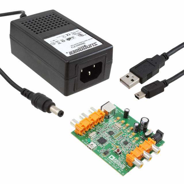
ADG2128 Data Sheet EVALUATION BOARD The ADG2128 evaluation board allows designers to evaluate the USING THE ADG2128 EVALUATION BOARD high performance ADG2128 8 × 12 switch array with minimum The ADG2128 evaluation kit is a test system designed to effort. simplify the evaluation of the ADG2128. Each input/output of the part comes with a socket specifically chosen for easy The evaluation kit includes a populated, tested ADG2128 audio/video evaluation. An application note is also available printed circuit board. The evaluation board interfaces to the with the evaluation board and gives full information on USB port of a PC, or it can be used as a standalone evaluation operating the evaluation board. board. Software is available with the evaluation board that allows the user to easily program the ADG2128 through the USB POWER SUPPLY port. Schematics of the evaluation board are shown in Figure 36 The ADG2128 evaluation board can be operated with both and Figure 37. The software runs on any PC that has Microsoft® single and dual supplies. V and V are supplied externally by Windows® 2000 or Windows XP installed. DD SS the user. The V supply can be applied externally, or the USB L port can be used to power the digital circuitry. Rev. D | Page 24 of 28
Data Sheet ADG2128 SCHEMATICS T3 930-46450 T2 T1 C1022PF +3.3V C220.1UF 24LC648A0VCC7A1WP6A2SCL5VSSSDA U2 SDA SCL XTAL1 24 MHZC1722PF 1234 V +3.3 18192021222324254546474849505152 293031 1615 4 5 +3.3V R70R +3.3VC18C23 FFUU12..02 27351732453711 CCCCCCCCCCCCCCCCPB0/FD0VVVVVVVVAPB1/FD1PB2/FD242PB3/FD3RESET44PB4/FD4*WAKEUPPB5/FD5PB6/FD654CLKOUTPB7/FD7PD0/FD8PD1/FD99U3D-PD2/FD108CY7C68013-CSPD+PD3/FD11PD4/FD12PD5/FD1333PA0/INT0PD6/FD1434PD7/FD15PA1/INT135PA2/*SLOE36PA3/*WU237CTL0/*FLAGAPA4/FIFOADR038PA5/FIFOADR1CTL1/*FLAGB39PA6/*PKTENDCTL2/*FLAGC40PA7/*FLD/SLCS SDA1RDY0/*SLRDSCL2RDY1/*SLWR13XTALOUTIFCLK14RSVDDXTALINDNDDDDDDNNNNNNNGGGGGGGGA 626081361212455R1010K +3.3V R111KUF D43.3V +3.3V R675 C90.1UF C21C19C20 0.1UF0.1UF0.1UF C15C1410UF0.1 +3.3V R575 C410UF DGND +3.3V C7C8C6C5 0.1UF0.1UF0.1UF0.1UF 126C160.1UF3 J1USB-MINI-B1VBUS2D-3D+4IO5GND ADP3303-3.38OUT1IN17OUT2IN25ERRORSDNRGNDU54 D EL HI S C3 0.1UF B C1310UF S U 5V Figure 36. EVAL-ADG2128EB Schematic, USB Controller Section Rev. D | Page 25 of 28
ADG2128 Data Sheet VL 040-46450 J2-1 J2-2 J2-3 J2-4 D D S +3.3V 5K AVD AGN C276V310UFAVS VL C316V310UF + AVDD C216V10UF C260.1UF +0.1UFC30 + D1 C10.1UF SB SCL SDA U V 5 D DGND SCL SDA AVDD AGN AVSS VL T4 T5 10K 10K 10K 10K C2510UF6V3 + R28 R29 R30 R31 C240.1UF ET K1 K2 K3 S E R D D V A B A 2K2 2K2 C2910UF16V X10_X11- 4 X10_X11- 3 X8_X9-B 4 X8_X9-A 3 X6_X7-B 4 X6_X7-A 3 2 1 2 1 2 1 R9 R8 +C280.1UF R22 R23 R24 R25 R26 R27 D N G A 32 31 30 29 28 27 26 25 24 23 22 21 20 19 18 17 GND ESET A2 A1 A0 SCL SDA VL VDD NC X11 X10 X9 X8 X7 X6 P R C Y U1G2128 D VSS A NC X0 X1 X2 X3 X4 X5 Y0 Y1 Y2 Y3 Y4 Y5 Y6 Y7 AGND 1 2 3 4 5 6 7 8 9 10 11 12 13 14 15 16 VSS 6V310UFC12 + C110.1UF R1 R2 R3 R4 R12 R13 R14 R15 R16 R17 R18 R19 R20 R21 D N G D 1 2 1 2 1 2 1 2 1 2 1 2 1 2 A B 3 4 3 4 3 4 3 4 3 4 3 4 3 4 K4 X0_X1-A X0_X1-B X2_X3-A X2_X3-B X4_X5-A X4_X5-B Y0_Y1-A Y0_Y1-B Y2_Y3-A Y2_Y3-B Y4_Y5-A Y4_Y5-B Y6_Y7-A Y6_Y7-B S S AV Figure 37. EVAL-ADG2128EB Schematic, Chip Section Rev. D | Page 26 of 28
Data Sheet ADG2128 OUTLINE DIMENSIONS 5.10 0.30 5.00 SQ 0.25 PIN 1 4.90 0.18 INDICATOR PIN 1 25 32 INDICATOR 24 1 0.50 BSC EXPOSED 3.25 PAD 3.10 SQ 2.95 17 8 0.50 16 9 0.25 MIN TOP VIEW 0.40 BOTTOM VIEW 0.30 FOR PROPER CONNECTION OF 0.80 THE EXPOSED PAD, REFER TO 0.75 THE PIN CONFIGURATION AND 0.05 MAX FUNCTION DESCRIPTIONS 0.70 0.02 NOM SECTION OF THIS DATA SHEET. COPLANARITY 0.08 SEATING 0.20 REF PLANE COMPLIANT TO JEDEC STANDARDS MO-220-WHHD. 112408-A Figure 38. 32-Lead Lead Frame Chip Scale Package [LFCSP_WQ] 5 mm x 5 mm Body, Very Very Thin Quad (CP-32-7) Dimensions shown in millimeters ORDERING GUIDE Temperature Package Model1, 2 Range I2C Speed Package Description Option ADG2128BCPZ-REEL −40°C to +85°C 100 kHz, 400 kHz 32-Lead Lead Frame Chip Scale Package [LFCSP_WQ] CP-32-7 ADG2128BCPZ-REEL7 −40°C to +85°C 100 kHz, 400 kHz 32-Lead Lead Frame Chip Scale Package [LFCSP_WQ] CP-32-7 ADG2128BCPZ-HS-RL7 –40°C to +85°C 100 kHz, 400 kHz, 3.4 MHz 32-Lead Lead Frame Chip Scale Package [LFCSP_WQ] CP-32-7 ADG2128WBCPZ-REEL7 −40°C to +85°C 100 kHz, 400 kHz 32-Lead Lead Frame Chip Scale Package [LFCSP_WQ] CP-32-7 ADG2128YCPZ-REEL −40°C to +125°C 100 kHz, 400 kHz 32-Lead Lead Frame Chip Scale Package [LFCSP_WQ] CP-32-7 ADG2128YCPZ-REEL7 −40°C to +125°C 100 kHz, 400 kHz 32-Lead Lead Frame Chip Scale Package [LFCSP_WQ] CP-32-7 ADG2128YCPZ-HS-RL7 –40°C to +125°C 100 kHz, 400 kHz, 3.4 MHz 32-Lead Lead Frame Chip Scale Package [LFCSP_WQ] CP-32-7 EVAL-ADG2128EBZ Evaluation Board 1 Z = RoHS Compliant Part. 2 W = Qualified for Automotive Applications. AUTOMOTIVE PRODUCTS The ADG2128W models are available with controlled manufacturing to support the quality and reliability requirements of automotive applications. Note that these automotive models may have specifications that differ from the commercial models; therefore, designers should review the Specifications section of this data sheet carefully. Only the automotive grade products shown are available for use in automotive applications. Contact your local Analog Devices account representative for specific product ordering information and to obtain the specific Automotive Reliability reports for these models. Rev. D | Page 27 of 28
ADG2128 Data Sheet NOTES Purchase of licensed I2C components of Analog Devices or one of its sublicensed Associated Companies conveys a license for the purchaser under the Philips I2C Patent Rights to use these components in an I2C system, provided that the system conforms to the I2C Standard Specification as defined by Philips. ©2006–2012 Analog Devices, Inc. All rights reserved. Trademarks and registered trademarks are the property of their respective owners. D05464-0-10/12(D) Rev. D | Page 28 of 28