ICGOO在线商城 > 射频/IF 和 RFID > RF 评估和开发套件,板 > EVAL-ADF5002EB2Z
 Datasheet下载
- 型号: EVAL-ADF5002EB2Z
- 制造商: Analog
- 库位|库存: xxxx|xxxx
- 要求:
| 数量阶梯 | 香港交货 | 国内含税 |
| +xxxx | $xxxx | ¥xxxx |
查看当月历史价格
查看今年历史价格
EVAL-ADF5002EB2Z产品简介:
ICGOO电子元器件商城为您提供EVAL-ADF5002EB2Z由Analog设计生产,在icgoo商城现货销售,并且可以通过原厂、代理商等渠道进行代购。 EVAL-ADF5002EB2Z价格参考。AnalogEVAL-ADF5002EB2Z封装/规格:RF 评估和开发套件,板, 。您可以下载EVAL-ADF5002EB2Z参考资料、Datasheet数据手册功能说明书,资料中有EVAL-ADF5002EB2Z 详细功能的应用电路图电压和使用方法及教程。
| 参数 | 数值 |
| 产品目录 | |
| 描述 | BOARD EVALUATION FOR ADF5002时钟和定时器开发工具 EVAL BRD ADF5002 |
| 产品分类 | |
| 品牌 | Analog Devices |
| 产品手册 | |
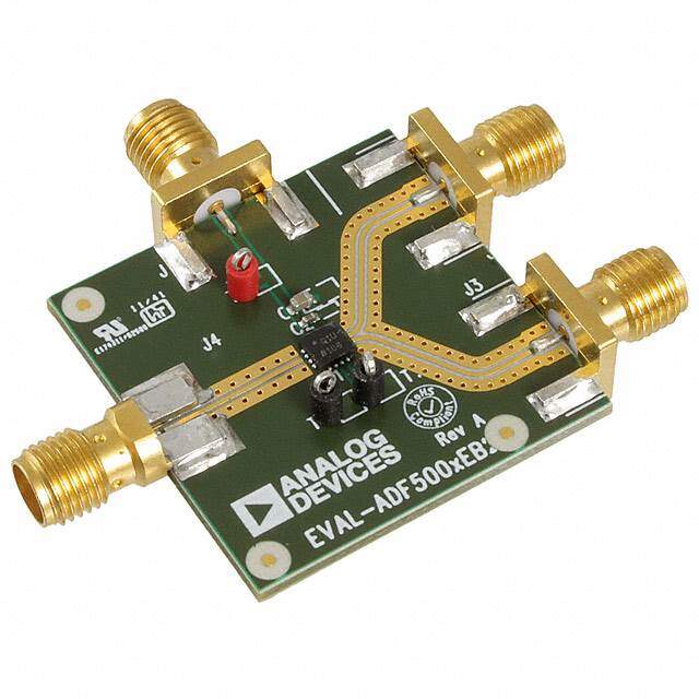
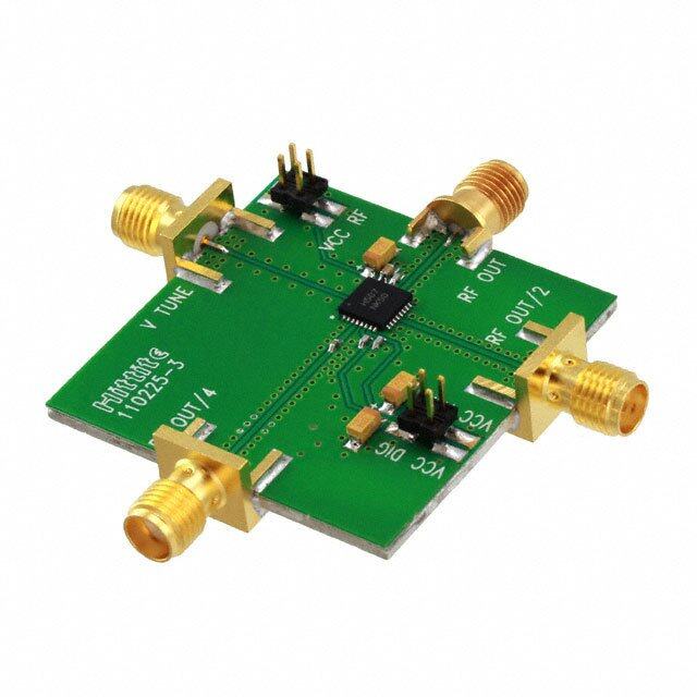
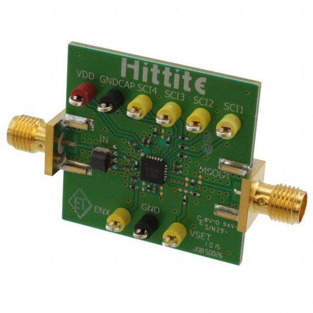
| 产品图片 |
|
| rohs | 符合RoHS无铅 / 符合限制有害物质指令(RoHS)规范要求 |
| 产品系列 | 模拟与数字IC开发工具,时钟和定时器开发工具,Analog Devices EVAL-ADF5002EB2Z- |
| 数据手册 | |
| 产品型号 | EVAL-ADF5002EB2Z |
| 产品 | Evaluation Boards |
| 产品种类 | 时钟和定时器开发工具 |
| 其它名称 | EVALADF5002EB2Z |
| 商标 | Analog Devices |
| 封装 | Bulk |
| 工作电源电压 | 3.3 V |
| 工作电源电流 | 30 mA |
| 工具用于评估 | ADF5002 |
| 工厂包装数量 | 1 |
| 所含物品 | 板 |
| 描述/功能 | RF prescaler |
| 标准包装 | 1 |
| 类型 | Clock Distributions |
| 视频文件 | http://www.digikey.cn/classic/video.aspx?PlayerID=1364138032001&width=640&height=505&videoID=2245193150001 |
| 设计资源 | http://www.analog.com/static/imported-files/eval_boards/EVAL-ADF500xEB2Z_RevA_Gerbers.zip |
| 配套使用产品/相关产品 | ADF5002 |
| 频率 | 18 GHz |


PDF Datasheet 数据手册内容提取
4 GHz to 18 GHz Divide-by-8 Prescaler ADF5002 FEATURES FUNCTIONAL BLOCK DIAGRAM Divide-by-8 prescaler CE High frequency operation: 4 GHz to 18 GHz ADF5002 Integrated RF decoupling capacitors BIAS VDDx Low power consumption Active mode: 30 mA 100Ω 100Ω Power-down mode: 7 mA 1pF Low phase noise: −153 dBc/Hz 3pF DIVIDE RFOUT RFIN BY 8 Single dc supply: 3.3 V compatible with ADF4xxx PLLs RFOUT 1pF Temperature range: −40°C to +105°C 50Ω Small package: 3 mm × 3 mm LFCSP APPLICATIONS GND 08753-001 Figure 1. PLL frequency range extender Point-to-point radios VSAT radios Communications test equipment GENERAL DESCRIPTION The ADF5002 prescaler is a low noise, low power, fixed RF divider block that can be used to divide down frequencies as high as 18 GHz to a lower frequency suitable for input to a PLL IC, such as the ADF4156 or the ADF4106. The ADF5002 provides a divide-by-8 function. The ADF5002 operates from a 3.3 V supply and has differential 100 Ω RF outputs to allow direct interface to the differential RF inputs of PLLs such as the ADF4156 and ADF4106. Rev. 0 Information furnished by Analog Devices is believed to be accurate and reliable. However, no responsibility is assumed by Analog Devices for its use, nor for any infringements of patents or other One Technology Way, P.O. Box 9106, Norwood, MA 02062-9106, U.S.A. rights of third parties that may result from its use. Specifications subject to change without notice. No license is granted by implication or otherwise under any patent or patent rights of Analog Devices. Tel: 781.329.4700 www.analog.com Trademarks and registered trademarks are the property of their respective owners. Fax: 781.461.3113 ©2010 Analog Devices, Inc. All rights reserved.
ADF5002 TABLE OF CONTENTS Features .............................................................................................. 1 Pin Configuration and Function Descriptions ..............................5 Applications ....................................................................................... 1 Typical Performance Characteristics ..............................................6 General Description ......................................................................... 1 Evaluation Board PCB ......................................................................7 Functional Block Diagram .............................................................. 1 PCB Material Stack-Up ................................................................7 Revision History ............................................................................... 2 Bill of Materials ..............................................................................7 Specifications ..................................................................................... 3 Application Circuit ............................................................................8 Absolute Maximum Ratings ............................................................ 4 Outline Dimensions ..........................................................................9 ESD Caution .................................................................................. 4 Ordering Guide .............................................................................9 REVISION HISTORY 6/10—Revision 0: Initial Version Rev. 0 | Page 2 of 12
ADF5002 SPECIFICATIONS VDD1 = VDD2 = 3.3 V ± 10%, GND = 0 V; dBm referred to 50 Ω; T = T to T , unless otherwise noted. Operating temperature A MIN MAX range is −40°C to +105°C. Table 1. Parameter Min Typ Max Unit Test Conditions/Comments RF CHARACTERISTICS Input Frequency 4 18 GHz RF Input Sensitivity −10 +10 dBm 4 GHz to 18 GHz Output Power −10 −5 dBm Single-ended output connected into a 50 Ω load −7 −2 dBm Differential outputs connected into a 100 Ω differential load Output Voltage Swing 200 330 mV p-p Peak-to-peak voltage swing on each single-ended output, connected into a 50 Ω load 400 660 mV p-p Peak-to-peak voltage swing on differential output, connected into a 100 Ω differential load 1000 mV p-p Peak-to-peak voltage swing on each single-ended output, no load condition Phase Noise −153 dBc/Hz Input frequency (f ) = 12 GHz, offset = 100 kHz IN Reverse Leakage −60 dBm RF input power (P ) = 0 dBm, RF = 4 GHz IN OUT Second Harmonic Content −38 dBc Third Harmonic Content −12 dBc Fourth Harmonic Content −20 dBc Fifth Harmonic Content −19 dBc CE INPUT Input High Voltage, V 2.2 V IH Input Low Voltage, V 0.3 V IL POWER SUPPLIES Voltage Supply 3.0 3.3 3.6 V I (I + I ) DD DD1 DD2 Active 30 60 mA CE is high Power-Down 7 25 mA CE is low Rev. 0 | Page 3 of 12
ADF5002 ABSOLUTE MAXIMUM RATINGS Table 2. This device is a high performance RF integrated circuit with Parameter Rating an ESD rating of 2 kV, human body model (HBM), and is ESD VDDx to GND −0.3 V to +3.9 V sensitive. Proper precautions should be taken for handling and RFIN 10 dBm assembly. Operating Temperature Range Industrial (B Version) −40°C to +105°C ESD CAUTION Storage Temperature Range −65°C to +150°C Maximum Junction Temperature 150°C LFCSP Thermal Impedance Junction-to-Ambient (θ ) 90°C/W JA Junction-to-Case (θ ) 30°C/W JC Peak Temperature 260°C Time at Peak Temperature 40 sec Stresses above those listed under Absolute Maximum Ratings may cause permanent damage to the device. This is a stress rating only; functional operation of the device at these or any other conditions above those indicated in the operational section of this specification is not implied. Exposure to absolute maximum rating conditions for extended periods may affect device reliability. Rev. 0 | Page 4 of 12
ADF5002 PIN CONFIGURATION AND FUNCTION DESCRIPTIONS D 1D 2D D N D D N G V V G 6 5 4 3 1 1 1 1 PIN 1 GND 1 INDICATOR 12GND RFIN 2 ADF5002 11RFOUT GND 3 TOP VIEW 10RFOUT GND 4 (Not to Scale) 9 GND 5 6 7 8 D C E D N N C N G G NOTES 12 .. TNCHCOE N= NE NEXOCP OTCEOSDENDNTOEPCA GTDN.DDL.E MUST BE 08753-002 Figure 2. Pin Configuration Table 3. Pin Function Descriptions Pin No. Mnemonic Description 1, 3, 4, 5, 8, 9, GND RF Ground. All ground pins should be tied together. 12, 13, 16 2 RFIN Single-Ended 50 Ω Input to the RF Prescaler. This pin is ac-coupled internally via a 3 pF capacitor. 6 NC No Connect. This pin can be left unconnected. 7 CE Chip Enable. This pin is active high. When CE is brought low, the part enters power-down mode. If this functionality is not required, the pin can be left unconnected because it is pulled up internally through a weak pull-up resistor. 10 RFOUT Divided-Down Output of the Prescaler. This pin has an internal 100 Ω load resistor tied to VDD2 and an ac-coupling capacitor of 1 pF. 11 RFOUT Complementary Divided-Down Output of the Prescaler. This pin has an internal 100 Ω load resistor tied to VDD2 and an ac-coupling capacitor of 1 pF. 14 VDD2 Voltage Supply for the Output Stage. This pin should be decoupled to ground with a 0.1 μF capacitor in parallel with a 10 pF capacitor and can be tied directly to VDD1. 15 VDD1 Voltage Supply for the Input Stage and Divider Block. This pin should be decoupled to ground with a 0.1 μF capacitor in parallel with a 10 pF capacitor. EPAD The LFCSP has an exposed paddle that must be connected to GND. Rev. 0 | Page 5 of 12
ADF5002 TYPICAL PERFORMANCE CHARACTERISTICS 0 –5 –10 –10 m) –15 B m) WER (d –20 ER (dB –20 O W –25 MINIMUM INPUT P ––4300 VVVDDDDDD === 333...036VVV HARMONIC PO –––343005 FTFIHIRFITSRHTD HHHAAARRRMMMOOONNNIIICCC –50 SEVENTH HARMONIC –45 EIGHTH HARMONIC NINTH HARMONIC ELEVENTH HARMONIC –60 –50 0 5 IN1P0UTFREQ1U5ENCY(G2H0z) 25 30 8753-0030 2.4 2.7 VDD3.x0 (V) 3.3 3.6 08753-006 Figure 3. RF Input Sensitivity Figure 6. RF Output Harmonic Content vs. VDDx 40 0 IDD_IN –1 35 IDD_OUT –2 fIN= 10GHz, VDD= 3.3V 30 m) –3 B I (mA)DDx2250 T POWER (d –––456 15 U P UT –7 10 O –8 5 fIN= 10GHz, PIN= 0dBm –9 02.5 2.7 2.9 3.1VDDx3 (.V3) 3.5 3.7 3.9 08753-004 –100 5 IN1P0UT FREQ1U5ENCY (G2H0z) 25 30 8753-0070 Figure 4. IDD1 and IDD2 vs. VDDx, fIN = 10 GHz, PIN = 0 dBm Figure 7. RF Output Power vs. RF Input Frequency, fIN = 10 GHz, VDD = 3.3 V 0 –2 –4 m) –6 B d R ( –8 E W O –10 P UT –12 P T OU –14 –16 –18 fIN= 10GHz, PIN= 0dBm –20 2.5 2.7 2.9 3.1VDDx3 (.V3) 3.5 3.7 3.9 08753-005 Figure 5. RF Output Power (Single-Ended) vs. VDDx, fIN = 10 GHz, PIN = 0 dBm Rev. 0 | Page 6 of 12
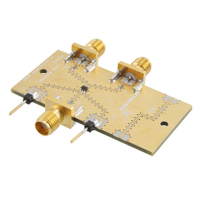
ADF5002 EVALUATION BOARD PCB The evaluation board has four connectors as shown in Figure 8. PCB MATERIAL STACK-UP The RF input connector (J4) is a high frequency precision SMA The evaluation board is built using Rogers RO4003C material connector from Emerson. This connector is mechanically (0.008 inch). RF track widths are 0.015 inch to achieve a controlled compatible with SMA, 3.5 mm, and 2.92 mm cables. 50 Ω characteristic impedance. The complete PCB stack-up is shown in Figure 9. 1.5oz (53µm) FINISHED COPPER ROGERS RO4003C LAMINATE 0.008” εr = 3.38. STARTING COPPER WEIGHT 0.5oz/0.5oz 0.5oz (18µm) FINISHED COPPER 0.062” ± 0.003” FR4 PREPREG COPPER TO COPPER 0.0372” 08753-008 Figure 8. Evaluation Board Silkscreen—Top View 0.5oz (18µm) FINISHED COPPER The evaluation board is powered from a single 3.0 V to 3.6 V supply, which should be connected to the J1 SMA connector. ROGERS RO4003C LAMINATE 0.008” The power supply can also be connected using the T3 (VDDx) εr = 3.38. STARTING COPPER WEIGHT 0.5oz/0.5oz and T2 (GND) test points. The differential RF outputs are brought out on the J2 and J3 1.5oz (53µm) FINISHED COPPER 08753-009 SMA connectors. If only one of the outputs is being used, the Figure 9. Evaluation Board PCB Layer Stack-Up unused output should be correctly terminated using a 50 Ω SMA termination. The chip enable (CE) pin can be controlled using the T1 test point. If this function is not required, the test point can be left unconnected. BILL OF MATERIALS Table 4. Qty Reference Designator Description Supplier Part Number 1 C1 0.1 μF, 0603 capacitor Murata GRM188R71H104KA93D 1 C2 10 pF, 0402 capacitor Murata GRM1555C1H100JZ01D 3 J1, J2, J3 SMA RF connector Emerson 142-0701-851 1 J4 SMA RF connector Emerson 142-0761-801 3 T1, T2, T3 Test points Vero 20-2137 1 U1 ADF5002 RF prescaler Analog Devices, Inc. ADF5002BCPZ Rev. 0 | Page 7 of 12
ADF5002 APPLICATION CIRCUIT The ADF5002 can be connected either single-ended or differ- The positive input pin of the OP184 is biased at half the ADF4156 entially to any of the Analog Devices PLL family of ICs. It is charge pump supply (V ). This can be easily achieved using a P recommended that a differential connection be used for best simple resistor divider, ensuring sufficient decoupling close to performance and to achieve maximum power transfer. The the +IN A pin of the OP184. This configuration, in turn, allows application circuit shown in Figure 10 shows the ADF5002 the use of a single positive supply for the op amp. Alternatively, used as the RF prescaler in a microwave 16 GHz PLL loop. The to optimize performance by ensuring a clean bias voltage, a low ADF5002 divides the 16 GHz RF signal down to 2 GHz, which noise regulator such as the ADP150 can be used to power the is input differentially into the ADF4156 PLL. An active filter resistor divider network or the +IN A pin directly. topology, using the OP184 op amp, is used to provide the wide tuning ranges typically required by microwave VCOs. 1.8nF 10pF 0.1µF 330Ω 47nF VDD1 VDD2 ADF4156 DECOUPLING PLL INTEGRATED ADF5002 RFOUT RFINA 220Ω RFIN PRESCALER CP OP184 1kΩ RFOUT RFINB 820pF VP/2 OP AMP GND 1µF 1.8nF MICROWAVE 6dB ATTENUATION PAD VCO 18Ω RFOUT VTUNE 37Ω 150Ω 150Ω 18Ω 16GHz OUT 08753-010 Figure 10. ADF5002 Used as the RF Prescaler in a Microwave 16 GHz PLL Loop Rev. 0 | Page 8 of 12
ADF5002 OUTLINE DIMENSIONS 3.10 0.30 3.00 SQ 0.25 PIN 1 2.90 0.18 INDICATOR PIN 1 0.50 13 16 INDICATOR BSC 12 1 EXPOSED 1.60 PAD 1.50 SQ 1.40 9 4 0.45 8 5 0.25 MIN TOP VIEW 0.40 BOTTOM VIEW 0.35 0.80 FOR PROPER CONNECTION OF 0.75 THE EXPOSED PAD, REFER TO 0.05 MAX THE PIN CONFIGURATION AND 0.70 0.02 NOM FUNCTION DESCRIPTIONS SECTION OF THIS DATA SHEET. COPLANARITY SEATING 0.08 PLANE 0.20 REF COMPLIANTTOJEDEC STANDARDS MO-220-WEED-6. 111808-A Figure 11. 16-Lead Lead Frame Chip Scale Package [LFCSP_WQ] 3 mm × 3 mm Body, Very Very Thin Quad (CP-16-18) Dimensions shown in millimeters ORDERING GUIDE Model1 Temperature Range Package Description Package Option Branding ADF5002BCPZ −40°C to +105°C 16-Lead Lead Frame Chip Scale Package (LFCSP_WQ) CP-16-18 Q1U ADF5002BCPZ-RL7 −40°C to +105°C 16-Lead Lead Frame Chip Scale Package (LFCSP_WQ), CP-16-18 Q1U 7” Tape and Reel EVAL-ADF5002EB2Z Evaluation Board 1 Z = RoHS Compliant Part. Rev. 0 | Page 9 of 12
ADF5002 NOTES Rev. 0 | Page 10 of 12
ADF5002 NOTES Rev. 0 | Page 11 of 12
ADF5002 NOTES ©2010 Analog Devices, Inc. All rights reserved. Trademarks and registered trademarks are the property of their respective owners. D08753-0-6/10(0) Rev. 0 | Page 12 of 12
Mouser Electronics Authorized Distributor Click to View Pricing, Inventory, Delivery & Lifecycle Information: A nalog Devices Inc.: ADF5002BCPZ EVAL-ADF5002EB2Z ADF5002BCPZ-RL7