ICGOO在线商城 > 开发板,套件,编程器 > 评估和演示板和套件 > EVAL-ADF4351EB1Z
- 型号: EVAL-ADF4351EB1Z
- 制造商: Analog
- 库位|库存: xxxx|xxxx
- 要求:
| 数量阶梯 | 香港交货 | 国内含税 |
| +xxxx | $xxxx | ¥xxxx |
查看当月历史价格
查看今年历史价格
EVAL-ADF4351EB1Z产品简介:
ICGOO电子元器件商城为您提供EVAL-ADF4351EB1Z由Analog设计生产,在icgoo商城现货销售,并且可以通过原厂、代理商等渠道进行代购。 EVAL-ADF4351EB1Z价格参考。AnalogEVAL-ADF4351EB1Z封装/规格:评估和演示板和套件, ADF4351 Frequency Synthesizer Timing Evaluation Board。您可以下载EVAL-ADF4351EB1Z参考资料、Datasheet数据手册功能说明书,资料中有EVAL-ADF4351EB1Z 详细功能的应用电路图电压和使用方法及教程。
| 参数 | 数值 |
| 产品目录 | 编程器,开发系统嵌入式解决方案 |
| 描述 | BOARD 1 EVAL FOR ADF4351时钟和定时器开发工具 EVAL BRD - ADF4351 |
| 产品分类 | |
| 品牌 | Analog Devices |
| 产品手册 | |
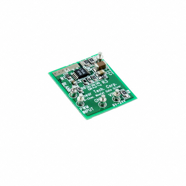
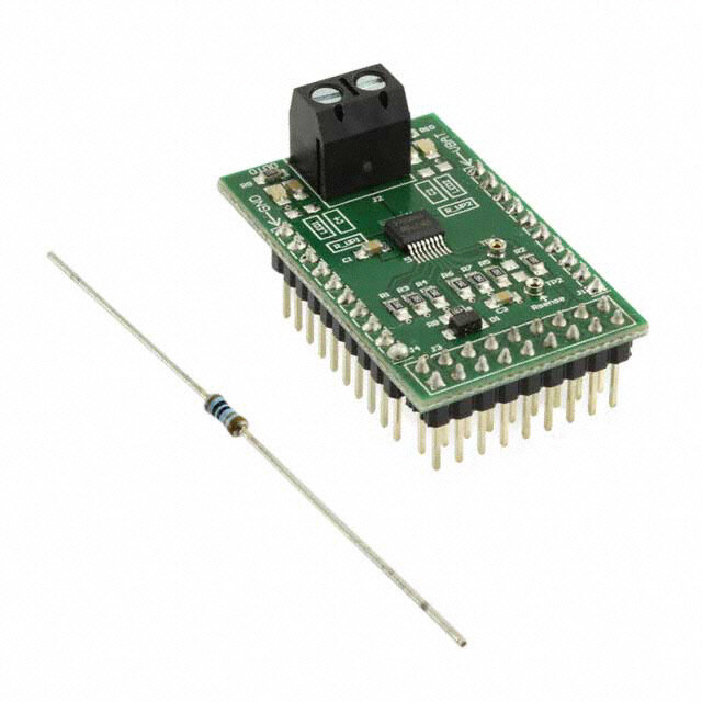
| 产品图片 |
|
| rohs | 符合RoHS不受无铅要求限制 / 不受限制有害物质指令(RoHS)规范要求限制 |
| 产品系列 | 模拟与数字IC开发工具,时钟和定时器开发工具,Analog Devices EVAL-ADF4351EB1Z- |
| 数据手册 | |
| 产品型号 | EVAL-ADF4351EB1Z |
| 主要属性 | 单路分数-N PLL |
| 主要用途 | 计时,频率合成器 |
| 产品 | Evaluation Boards |
| 产品种类 | 时钟和定时器开发工具 |
| 使用的IC/零件 | ADF4351 |
| 其它名称 | EVALADF4351EB1Z |
| 商标 | Analog Devices |
| 封装 | Bulk |
| 嵌入式 | 否 |
| 工作电源电压 | 3.75 V to 5.5 V |
| 工作电源电流 | 110 mA |
| 工具用于评估 | ADF4351 |
| 工厂包装数量 | 1 |
| 所含物品 | 板,线缆,软件 |
| 接口类型 | USB |
| 描述/功能 | Self contained board including PLL, VCO, loop filter 35 kHz, 25 MHz TCXO reference |
| 标准包装 | 1 |
| 特色产品 | http://www.digikey.cn/product-highlights/zh/cn0285-direct-conversion-transmitters/50283 |
| 类型 | PLL Synthesizers / Multipliers / Dividers |
| 视频文件 | http://www.digikey.cn/classic/video.aspx?PlayerID=1364138032001&width=640&height=505&videoID= 2474683249001 |
| 辅助属性 | - |
| 频率 | 250 MHz, 4.4 GHz |




- 商务部:美国ITC正式对集成电路等产品启动337调查
- 曝三星4nm工艺存在良率问题 高通将骁龙8 Gen1或转产台积电
- 太阳诱电将投资9.5亿元在常州建新厂生产MLCC 预计2023年完工
- 英特尔发布欧洲新工厂建设计划 深化IDM 2.0 战略
- 台积电先进制程称霸业界 有大客户加持明年业绩稳了
- 达到5530亿美元!SIA预计今年全球半导体销售额将创下新高
- 英特尔拟将自动驾驶子公司Mobileye上市 估值或超500亿美元
- 三星加码芯片和SET,合并消费电子和移动部门,撤换高东真等 CEO
- 三星电子宣布重大人事变动 还合并消费电子和移动部门
- 海关总署:前11个月进口集成电路产品价值2.52万亿元 增长14.8%
PDF Datasheet 数据手册内容提取
Wideband Synthesizer with Integrated VCO Data Sheet ADF4351 FEATURES GENERAL DESCRIPTION Output frequency range: 35 MHz to 4400 MHz The ADF4351 allows implementation of fractional-N or integer-N Fractional-N synthesizer and integer-N synthesizer phase-locked loop (PLL) frequency synthesizers when used with Low phase noise VCO an external loop filter and external reference frequency. Programmable divide-by-1/-2/-4/-8/-16/-32/-64 output The ADF4351 has an integrated voltage controlled oscillator (VCO) Typical jitter: 0.3 ps rms with a fundamental output frequency ranging from 2200 MHz to Typical EVM at 2.1 GHz: 0.4% 4400 MHz. In addition, divide-by-1/-2/-4/-8/-16/-32/-64 circuits Power supply: 3.0 V to 3.6 V allow the user to generate RF output frequencies as low as 35 MHz. Logic compatibility: 1.8 V For applications that require isolation, the RF output stage can be Programmable dual-modulus prescaler of 4/5 or 8/9 muted. The mute function is both pin- and software-controllable. Programmable output power level An auxiliary RF output is also available, which can be powered RF output mute function down when not in use. 3-wire serial interface Analog and digital lock detect Control of all on-chip registers is through a simple 3-wire interface. Switched bandwidth fast lock mode The device operates with a power supply ranging from 3.0 V to Cycle slip reduction 3.6 V and can be powered down when not in use. APPLICATIONS Wireless infrastructure (W-CDMA, TD-SCDMA, WiMAX, GSM, PCS, DCS, DECT) Test equipment Wireless LANs, CATV equipment Clock generation FUNCTIONAL BLOCK DIAGRAM SDVDD AVDD DVDD VP RSET VVCO MULTIPLEXER MUXOUT 10-BIT R ÷2 ×2 COUNTER DIVIDER REFIN DOUBLER LOCK DETECT FA SSWT ILTOCHCK SW CLK LD DATA DATA REGISTER FUNCTION CHARGE LE LATCH PUMP CPOUT PHASE COMPARATOR VTUNE VREF VCO VCOM INTEGER FRACTION MODULUS CORE TEMP VALUE VALUE VALUE RFOUTA+ THIRD-ORDER ÷1/2/4/8/16/ OUTPUT INFTREARCPTOIOLANTAOLR 32/64 STAGE RFOUTA– ER PDBRF X E N COUNTER LTIPL OSUTTAPGUET RRFFOOUUTTBB+– U M MULTIPLEXER ADF4351 CE AGND DGND CPGND SDGND AGNDVCO 09800-001 Figure 1. Rev. A Document Feedback Information furnished by Analog Devices is believed to be accurate and reliable. However, no responsibility is assumed by Analog Devices for its use, nor for any infringements of patents or other One Technology Way, P.O. Box 9106, Norwood, MA 02062-9106, U.S.A. rights of third parties that may result from its use. Specifications subject to change without notice. No license is granted by implication or otherwise under any patent or patent rights of Analog Devices. Tel: 781.329.4700 ©2012–2017 Analog Devices, Inc. All rights reserved. Trademarks and registered trademarks are the property of their respective owners. Technical Support www.analog.com
ADF4351 Data Sheet TABLE OF CONTENTS Features .............................................................................................. 1 Register 1 ..................................................................................... 18 Applications ....................................................................................... 1 Register 2 ..................................................................................... 18 General Description ......................................................................... 1 Register 3 ..................................................................................... 19 Functional Block Diagram .............................................................. 1 Register 4 ..................................................................................... 20 Revision History ............................................................................... 2 Register 5 ..................................................................................... 20 Specifications ..................................................................................... 3 Register Initialization Sequence ............................................... 20 Timing Characteristics ................................................................ 5 RF Synthesizer—A Worked Example ...................................... 21 Absolute Maximum Ratings ............................................................ 6 Reference Doubler and Reference Divider ............................. 21 Transistor Count ........................................................................... 6 12-Bit Programmable Modulus ................................................ 21 Thermal Resistance ...................................................................... 6 Cycle Slip Reduction for Faster Lock Times ........................... 22 ESD Caution .................................................................................. 6 Spurious Optimization and Fast Lock ..................................... 22 Pin Configuration and Function Descriptions ............................. 7 Fast Lock Timer and Register Sequences ................................ 22 Typical Performance Characteristics ............................................. 9 Fast Lock Example ..................................................................... 22 Circuit Description ......................................................................... 11 Fast Lock Loop Filter Topology ................................................ 23 Reference Input Section ............................................................. 11 Spur Mechanisms ....................................................................... 23 RF N Divider ............................................................................... 11 Spur Consistency and Fractional Spur Optimization ........... 24 Phase Frequency Detector (PFD) and Charge Pump ............ 11 Phase Resync ............................................................................... 24 MUXOUT and Lock Detect ...................................................... 12 Applications Information .............................................................. 25 Input Shift Registers ................................................................... 12 Direct Conversion Modulator .................................................. 25 Program Modes .......................................................................... 12 Interfacing to the ADuC70xx and the ADSP-BF527 ............. 26 VCO.............................................................................................. 12 PCB Design Guidelines for a Chip Scale Package ................. 26 Output Stage ................................................................................ 13 Output Matching ........................................................................ 27 Register Maps .................................................................................. 14 Outline Dimensions ....................................................................... 28 Register 0 ..................................................................................... 18 Ordering Guide .......................................................................... 28 REVISION HISTORY 1/2017—Rev. 0 to Rev. A Changed CP-32-2 to CP-32-7 ...................................... Throughout Change to Figure 3 ........................................................................... 7 Updated Outline Dimension ......................................................... 28 Changes to Ordering Guide .......................................................... 28 5/2012—Revision 0: Initial Version Rev. A | Page 2 of 28
Data Sheet ADF4351 SPECIFICATIONS AV = DV = V = SDV = V = 3.3 V ± 10%; AGND = DGND = 0 V; T = T to T , unless otherwise noted. Operating DD DD VCO DD P A MIN MAX temperature range is −40°C to +85°C. Table 1. Parameter Min Typ Max Unit Test Conditions/Comments REF CHARACTERISTICS IN Input Frequency 10 250 MHz For f < 10 MHz, ensure slew rate > 21 V/µs Input Sensitivity 0.7 AV V p-p Biased at AV /2; ac coupling ensures AV /2 bias DD DD DD Input Capacitance 10 pF Input Current ±60 µA PHASE FREQUENCY DETECTOR (PFD) Phase Detector Frequency 32 MHz Fractional-N 45 MHz Integer-N (band select enabled) 90 MHz Integer-N (band select disabled) CHARGE PUMP I Sink/Source1 R = 5.1 kΩ CP SET High Value 5 mA Low Value 0.312 mA R Range 3.9 10 kΩ SET Sink and Source Current Matching 2 % 0.5 V ≤ V ≤ 2.5 V CP I vs. V 1.5 % 0.5 V ≤ V ≤ 2.5 V CP CP CP I vs. Temperature 2 % V = 2.0 V CP CP LOGIC INPUTS Input High Voltage, V 1.5 V INH Input Low Voltage, V 0.6 V INL Input Current, I /I ±1 µA INH INL Input Capacitance, C 3.0 pF IN LOGIC OUTPUTS Output High Voltage, V DV − 0.4 V CMOS output selected OH DD Output High Current, I 500 µA OH Output Low Voltage, V 0.4 V I = 500 µA OL OL POWER SUPPLIES AV 3.0 3.6 V DD DV , V , SDV , V AV These voltages must equal AV DD VCO DD P DD DD DI + AI 2 21 27 mA DD DD Output Dividers 6 to 36 mA Each output divide-by-2 consumes 6 mA I 2 70 80 mA VCO I 2 21 26 mA RF output stage is programmable RFOUT Low Power Sleep Mode 7 10 µA RF OUTPUT CHARACTERISTICS VCO Output Frequency 2200 4400 MHz Fundamental VCO mode Minimum VCO Output Frequency 34.375 MHz 2200 MHz fundamental output and Using Dividers divide-by-64 selected VCO Sensitivity, K 40 MHz/V V Frequency Pushing (Open-Loop) 1 MHz/V Frequency Pulling (Open-Loop) 90 kHz Into 2.00 VSWR load Harmonic Content (Second) −19 dBc Fundamental VCO output −20 dBc Divided VCO output Harmonic Content (Third) −13 dBc Fundamental VCO output −10 dBc Divided VCO output Rev. A | Page 3 of 28
ADF4351 Data Sheet Parameter Min Typ Max Unit Test Conditions/Comments Minimum RF Output Power3 −4 dBm Programmable in 3 dB steps Maximum RF Output Power3 5 dBm Output Power Variation ±1 dB Minimum VCO Tuning Voltage 0.5 V Maximum VCO Tuning Voltage 2.5 V NOISE CHARACTERISTICS VCO Phase Noise Performance VCO noise is measured in open-loop conditions −89 dBc/Hz 10 kHz offset from 2.2 GHz carrier −114 dBc/Hz 100 kHz offset from 2.2 GHz carrier −134 dBc/Hz 1 MHz offset from 2.2 GHz carrier −148 dBc/Hz 5 MHz offset from 2.2 GHz carrier −86 dBc/Hz 10 kHz offset from 3.3 GHz carrier −111 dBc/Hz 100 kHz offset from 3.3 GHz carrier −134 dBc/Hz 1 MHz offset from 3.3 GHz carrier −145 dBc/Hz 5 MHz offset from 3.3 GHz carrier −83 dBc/Hz 10 kHz offset from 4.4 GHz carrier −110 dBc/Hz 100 kHz offset from 4.4 GHz carrier −131 dBc/Hz 1 MHz offset from 4.4 GHz carrier −145 dBc/Hz 5 MHz offset from 4.4 GHz carrier Normalized Phase Noise Floor PLL loop BW = 500 kHz (PN )4 SYNTH −220 dBc/Hz ABP = 6 ns −221 dBc/Hz ABP = 3 ns Normalized 1/f Noise (PN )5 10 kHz offset; normalized to 1 GHz 1_f −116 dBc/Hz ABP = 6 ns −118 dBc/Hz ABP = 3 ns In-Band Phase Noise −100 dBc/Hz 3 kHz from 2111.28 MHz carrier Integrated RMS Jitter6 0.27 ps Spurious Signals Due to PFD −80 dBc Frequency Level of Signal with RF Mute Enabled −40 dBm 1 ICP is internally modified to maintain constant loop gain over the frequency range. 2 TA = 25°C; AVDD = DVDD = VVCO = 3.3 V; prescaler = 8/9; fREFIN = 100 MHz; fPFD = 25 MHz; fRF = 4.4 GHz. 3 Using 50 Ω resistors to VVCO, into a 50 Ω load. Power measured with auxiliary RF output disabled. The current consumption of the auxiliary output is the same as for the main output. 4 The synthesizer phase noise floor is estimated by measuring the in-band phase noise at the output of the VCO and subtracting 20 log N (where N is the N divider value) and 10 log fPFD. To calculate in-band phase noise performance as seen at the VCO output, use the following formula: PNSYNTH = PNTOT − 10 log(fPFD) − 20 log N. 5 The PLL phase noise is composed of flicker (1/f) noise plus the normalized PLL noise floor. The formula for calculating the 1/f noise contribution at an RF frequency (fRF) and at a frequency offset (f) is given by PN = PN1_f + 10 log(10 kHz/f) + 20 log(fRF/1 GHz). Both the normalized phase noise floor and flicker noise are modeled in ADIsimPLL. 6 fREFIN = 122.88 MHz; fPFD = 30.72 MHz; VCO frequency = 4222.56 MHz; RFOUT = 2111.28 MHz; N = 137; loop BW = 60 kHz; ICP = 2.5 mA; low noise mode. The noise was measured with an EVAL-ADF4351EB1Z and the Rohde & Schwarz FSUP signal source analyzer. Rev. A | Page 4 of 28
Data Sheet ADF4351 TIMING CHARACTERISTICS AV = DV = V = SDV = V = 3.3 V ± 10%; AGND = DGND = 0 V; 1.8 V and 3 V logic levels used; T = T to T , unless DD DD VCO DD P A MIN MAX otherwise noted. Table 2. Parameter Limit Unit Description t 20 ns min LE setup time 1 t 10 ns min DATA to CLK setup time 2 t 10 ns min DATA to CLK hold time 3 t 25 ns min CLK high duration 4 t 25 ns min CLK low duration 5 t 10 ns min CLK to LE setup time 6 t 20 ns min LE pulse width 7 Timing Diagram t t 4 5 CLK t t 2 3 DB2 DB1 DB0 (LSB) DATA DB31 (MSB) DB30 (CONTROL BIT C3) (CONTROL BIT C2) (CONTROL BIT C1) t 7 LE t1 t6 LE 09800-002 Figure 2. Timing Diagram Rev. A | Page 5 of 28
ADF4351 Data Sheet ABSOLUTE MAXIMUM RATINGS T = 25°C, unless otherwise noted. This device is a high performance RF integrated circuit with an A ESD rating of <1.5 kV and is ESD sensitive. Proper precautions Table 3. should be taken for handling and assembly. Parameter Rating TRANSISTOR COUNT AV to GND1 −0.3 V to +3.9 V DD AVDD to DVDD −0.3 V to +0.3 V The transistor count for the ADF4351 is 36,955 (CMOS) and VVCO to GND1 −0.3 V to +3.9 V 986 (bipolar). V to AV −0.3 V to +0.3 V VCO DD THERMAL RESISTANCE Digital I/O Voltage to GND1 −0.3 V to V + 0.3 V DD Analog I/O Voltage to GND1 −0.3 V to VDD + 0.3 V Thermal impedance (θJA) is specified for a device with the REF to GND1 −0.3 V to V + 0.3 V exposed pad soldered to GND. IN DD Operating Temperature Range −40°C to +85°C Table 4. Thermal Resistance Storage Temperature Range −65°C to +125°C Package Type θ Unit JA Maximum Junction Temperature 150°C 32-Lead LFCSP (CP-32-7) 27.3 °C/W Reflow Soldering Peak Temperature 260°C Time at Peak Temperature 40 sec ESD CAUTION 1 GND = AGND = DGND = CPGND = SDGND = AGNDVCO = 0 V. Stresses at or above those listed under Absolute Maximum Ratings may cause permanent damage to the product. This is a stress rating only; functional operation of the product at these or any other conditions above those indicated in the operational section of this specification is not implied. Operation beyond the maximum operating conditions for extended periods may affect product reliability. Rev. A | Page 6 of 28
Data Sheet ADF4351 PIN CONFIGURATION AND FUNCTION DESCRIPTIONS T DVDDDGNDUXOUEFINVDDGNDDBRFD SSMRDDPL 21098765 33322222 CLK 1 24 VREF DATA 2 23 VCOM LE 3 ADF4351 22 RSET CE 4 TOP VIEW 21 AGNDVCO SW 5 (Not to Scale) 20 VTUNE VP 6 19 TEMP CPOUT 7 18 AGNDVCO CPGND 8 17 VVCO 910111213141516 D D O+−+− O AGNAVD NDVCAOUTAOUTBOUTBOUTVVC GFFFF ARRRR N1 . O TMTHUEESS TL FBCES CPO HNANSE ACNT EEDX PTOOS GENDD P.AD THAT 09800-003 Figure 3. Pin Configuration Table 5. Pin Function Descriptions Pin No. Mnemonic Description 1 CLK Serial Clock Input. Data is clocked into the 32-bit shift register on the CLK rising edge. This input is a high impedance CMOS input. 2 DATA Serial Data Input. The serial data is loaded MSB first with the three LSBs as the control bits. This input is a high impedance CMOS input. 3 LE Load Enable. When LE goes high, the data stored in the 32-bit shift register is loaded into the register that is selected by the three control bits. This input is a high impedance CMOS input. 4 CE Chip Enable. A logic low on this pin powers down the device and puts the charge pump into three-state mode. A logic high on this pin powers up the device, depending on the status of the power-down bits. 5 SW Fast Lock Switch. A connection should be made from the loop filter to this pin when using the fast lock mode. 6 V Charge Pump Power Supply. V must have the same value as AV . Place decoupling capacitors to the ground P P DD plane as close to this pin as possible. 7 CP Charge Pump Output. When enabled, this output provides ±I to the external loop filter. The output of the OUT CP loop filter is connected to V to drive the internal VCO. TUNE 8 CP Charge Pump Ground. This output is the ground return pin for CP . GND OUT 9 AGND Analog Ground. Ground return pin for AV . DD 10 AV Analog Power Supply. This pin ranges from 3.0 V to 3.6 V. Place decoupling capacitors to the analog ground DD plane as close to this pin as possible. AV must have the same value as DV . DD DD 11, 18, 21 A VCO Analog Ground. Ground return pins for the VCO. GNDVCO 12 RF A+ VCO Output. The output level is programmable. The VCO fundamental output or a divided-down version is OUT available. 13 RF A− Complementary VCO Output. The output level is programmable. The VCO fundamental output or a divided- OUT down version is available. 14 RF B+ Auxiliary VCO Output. The output level is programmable. The VCO fundamental output or a divided-down OUT version is available. 15 RF B− Complementary Auxiliary VCO Output. The output level is programmable. The VCO fundamental output or a OUT divided-down version is available. 16, 17 V Power Supply for the VCO. This pin ranges from 3.0 V to 3.6 V. Place decoupling capacitors to the analog VCO ground plane as close to these pins as possible. V must have the same value as AV . VCO DD 19 TEMP Temperature Compensation Output. Place decoupling capacitors to the ground plane as close to this pin as possible. 20 V Control Input to the VCO. This voltage determines the output frequency and is derived from filtering the CP TUNE OUT output voltage. Rev. A | Page 7 of 28
ADF4351 Data Sheet Pin No. Mnemonic Description 22 R Connecting a resistor between this pin and ground sets the charge pump output current. The nominal voltage SET bias at the R pin is 0.55 V. The relationship between I and R is as follows: SET CP SET I = 25.5/R CP SET where: R = 5.1 kΩ. SET I = 5 mA. CP 23 V Internal Compensation Node. Biased at half the tuning range. Place decoupling capacitors to the ground plane COM as close to this pin as possible. 24 V Reference Voltage. Place decoupling capacitors to the ground plane as close to this pin as possible. REF 25 LD Lock Detect Output Pin. A logic high output on this pin indicates PLL lock. A logic low output indicates loss of PLL lock. 26 PDB RF Power-Down. A logic low on this pin mutes the RF outputs. This function is also software controllable. RF 27 DGND Digital Ground. Ground return pin for DV . DD 28 DV Digital Power Supply. DV must have the same value as AV . Place decoupling capacitors to the ground DD DD DD plane as close to this pin as possible. 29 REF Reference Input. This CMOS input has a nominal threshold of AV /2 and a dc equivalent input resistance of IN DD 100 kΩ. This input can be driven from a TTL or CMOS crystal oscillator, or it can be ac-coupled. 30 MUXOUT Multiplexer Output. The multiplexer output allows the lock detect value, the N divider value, or the R counter value to be accessed externally. 31 SD Digital Σ-Δ Modulator Ground. Ground return pin for the Σ-Δ modulator. GND 32 SDV Power Supply Pin for the Digital Σ-Δ Modulator. SDV must have the same value as AV . Place decoupling DD DD DD capacitors to the ground plane as close to this pin as possible. EP Exposed Pad Exposed Pad. The LFCSP has an exposed pad that must be connected to GND. Rev. A | Page 8 of 28
Data Sheet ADF4351 TYPICAL PERFORMANCE CHARACTERISTICS –40 –90 DIV1 –50 DIV2 –100 DIV4 –60 DIV8 –70 –110 DIV16 Bc/Hz) –80 Bc/Hz) –120 DDIIVV3624 d –90 d E ( E ( S –100 S –130 OI OI SE N –110 SE N –140 A –120 A H H P –130 P –150 –140 –160 –150 –1601k 10k FRE1Q00UkENCY (Hz)1M 10M 09800-104 –1701k 10k FRE1Q00UkENCY (Hz)1M 10M 09800-107 Figure 4. Open-Loop VCO Phase Noise, 2.2 GHz Figure 7. Closed-Loop Phase Noise, Fundamental VCO and Dividers, VCO = 2.2 GHz, PFD = 25 MHz, Loop Filter Bandwidth = 63 kHz –40 –90 DIV1 –50 DIV2 –100 DIV4 –60 DIV8 –70 –110 DIV16 Bc/Hz) –80 Bc/Hz) –120 DDIIVV3624 d –90 d E ( E ( S –100 S –130 OI OI SE N –110 SE N –140 A –120 A H H P P –130 –150 –140 –160 –150 –160 –170 1k 10k FRE1Q00UkENCY (Hz)1M 10M 09800-105 1k 10k FRE1Q00UkENCY (Hz)1M 10M 09800-108 Figure 5. Open-Loop VCO Phase Noise, 3.3 GHz Figure 8. Closed-Loop Phase Noise, Fundamental VCO and Dividers, VCO = 3.3 GHz, PFD = 25 MHz, Loop Filter Bandwidth = 63 kHz –40 –90 DIV1 –50 DIV2 –100 DIV4 –60 DIV8 –70 –110 DIV16 Bc/Hz) –80 Bc/Hz) –120 DDIIVV3624 d –90 d E ( E ( S –100 S –130 OI OI SE N –110 SE N –140 A –120 A H H P –130 P –150 –140 –160 –150 –160 –170 1k 10k FRE1Q00UkENCY (Hz)1M 10M 09800-106 1k 10k FRE1Q00UkENCY (Hz)1M 10M 09800-109 Figure 6. Open-Loop VCO Phase Noise, 4.4 GHz Figure 9. Closed-Loop Phase Noise, Fundamental VCO and Dividers, VCO = 4.4 GHz, PFD = 25 MHz, Loop Filter Bandwidth = 63 kHz Rev. A | Page 9 of 28
ADF4351 Data Sheet –60 –60 –70 –70 –80 –80 Hz) –90 Hz) –90 c/ c/ dB –100 dB –100 E ( E ( OIS –110 OIS –110 N N E –120 E –120 S S A A PH –130 PH –130 –140 –140 –150 –150 –1601k 10k FRE1Q00UkENCY (Hz)1M 10M 09800-110 –1601k 10k FRE1Q00UkENCY (Hz)1M 10M 09800-113 Figure 10. Fractional-N Spur Performance, Low Noise Mode, W-CDMA Band; Figure 13. Fractional-N Spur Performance, Low Noise Mode, LTE Band; RFOUT = 2111.28 MHz, REFIN = 122.88 MHz, PFD = 30.72 MHz, Output Divide-by-2 RFOUT = 2646.96 MHz, REFIN = 122.88 MHz, PFD = 30.72 MHz; Loop Filter Selected; Loop Filter Bandwidth = 60 kHz, Channel Spacing = 240 kHz; Bandwidth = 60 kHz, Channel Spacing = 240 kHz; Phase Word = 9, RMS Phase Error = 0.21°, RMS Jitter = 0.27 ps, EVM = 0.37% RMS Phase Error = 0.28°, RMS Jitter = 0.29 ps, EVM = 0.49% –60 –60 –70 –70 –80 –80 Hz) –90 Hz) –90 c/ c/ dB –100 dB –100 E ( E ( OIS –110 OIS –110 N N E –120 E –120 S S A A PH –130 PH –130 –140 –140 –150 –150 –1601k 10k FRE1Q00UkENCY (Hz)1M 10M 09800-111 –1601k 10k FRE1Q00UkENCY (Hz)1M 10M 09800-114 Figure 11. Fractional-N Spur Performance, Low Spur Mode, W-CDMA Band; Figure 14. Fractional-N Spur Performance, Low Spur Mode, LTE Band; RFOUT = 2111.28 MHz, REFIN = 122.88 MHz, PFD = 30.72 MHz, Output Divide-by-2 RFOUT = 2646.96 MHz, REFIN = 122.88 MHz, PFD = 30.72 MHz; Selected; Loop Filter Bandwidth = 60 kHz, Channel Spacing = 240 kHz; Loop Filter Bandwidth = 60 kHz, Channel Spacing = 240 kHz; RMS Phase Error = 0.37°, RMS Jitter = 0.49 ps, EVM = 0.64% RMS Phase Error = 0.56°, RMS Jitter = 0.59 ps, EVM = 0.98% –60 –60 –70 –70 –80 –80 Hz) –90 Hz) –90 c/ c/ dB –100 dB –100 E ( E ( OIS –110 OIS –110 N N E –120 E –120 S S A A PH –130 PH –130 –140 –140 –150 –150 –1601k 10k FRE1Q00UkENCY (Hz)1M 10M 09800-112 –1601k 10k FRE1Q00UkENCY (Hz)1M 10M 09800-115 Figure 12. Fractional-N Spur Performance, Low Noise Mode, W-CDMA Band; Figure 15. Fractional-N Spur Performance, Low Noise Mode, W-CDMA Band; RFOUT = 2111.28 MHz, REFIN = 122.88 MHz, PFD = 30.72 MHz, Output Divide-by-2 RFOUT = 2646.96 MHz, REFIN = 122.88 MHz, PFD = 30.72 MHz; Selected; Loop Filter Bandwidth = 20 kHz, Channel Spacing = 240 kHz; Loop Filter Bandwidth = 20 kHz, Channel Spacing = 240 kHz; RMS Phase Error = 0.25°, RMS Jitter = 0.32 ps, EVM = 0.44% RMS Phase Error = 0.35°, RMS Jitter = 0.36 ps, EVM = 0.61% Rev. A | Page 10 of 28
Data Sheet ADF4351 CIRCUIT DESCRIPTION REFERENCE INPUT SECTION The PFD frequency (f ) equation is PFD The reference input stage is shown in Figure 16. The SW1 and fPFD = REFIN × [(1 + D)/(R × (1 + T))] (2) SW2 switches are normally closed. The SW3 switch is normally where: open. When power-down is initiated, SW3 is closed, and SW1 REF is the reference input frequency. IN and SW2 are opened. In this way, no loading of the REF pin IN D is the REF doubler bit (0 or 1). IN occurs during power-down. R is the preset divide ratio of the binary 10-bit programmable POWER-DOWN reference counter (1 to 1023). CONTROL T is the REF divide-by-2 bit (0 or 1). IN NC 100kΩ Integer-N Mode SW2 REFIN NC TO R COUNTER If FRAC = 0 and the DB8 (LDF) bit in Register 2 is set to 1, the BUFFER SW1 synthesizer operates in integer-N mode. The DB8 bit in Register 2 NO SW3 09800-005 should be set to 1 for integer-N digital lock detect. R Counter Figure 16. Reference Input Stage RF N DIVIDER The 10-bit R counter allows the input reference frequency (REF ) to be divided down to produce the reference clock IN The RF N divider allows a division ratio in the PLL feedback to the PFD. Division ratios from 1 to 1023 are allowed. path. The division ratio is determined by the INT, FRAC, and PHASE FREQUENCY DETECTOR (PFD) AND MOD values, which build up this divider (see Figure 17). CHARGE PUMP RF N DIVIDER N = INT + FRAC/MOD FROM The phase frequency detector (PFD) takes inputs from the VCO OUTPUT/ OUTPUT DIVIDERS TO PFD R counter and N counter and produces an output proportional N COUNTER to the phase and frequency difference between them. Figure 18 THIRD-ORDER is a simplified schematic of the phase frequency detector. FRACTIONAL INTERPOLATOR UP HIGH D1 Q1 INT FRAC MOD U1 VALUE VALUE VALUE +IN CLR1 Figure 17. RF N Divider 09800-006 DELAY U3 CHPUAMRGPE CPOUT INT, FRAC, MOD, and R Counter Relationship The INT, FRAC, and MOD values, in conjunction with the CLR2 DOWN R counter, make it possible to generate output frequencies that HIGH D2 Q2 atiroen s,p saecee dth bey R fFra Scytinotnhse osifz tehre— PAF DW forerkqeude nEcxya. mFoprl em soercet iionnfo. rma- –IN U2 09800-007 Figure 18. PFD Simplified Schematic The RF VCO frequency (RF ) equation is OUT The PFD includes a programmable delay element that sets the RF = f × (INT + (FRAC/MOD)) (1) OUT PFD width of the antibacklash pulse (ABP). This pulse ensures that where: there is no dead zone in the PFD transfer function. Bit DB22 in RFOUT is the output frequency of the voltage controlled oscillator Register 3 (R3) is used to set the ABP as follows: (VCO). When Bit DB22 is set to 0, the ABP width is programmed to INT is the preset divide ratio of the binary 16-bit counter (23 to 6 ns, the recommended value for fractional-N applications. 65,535 for the 4/5 prescaler; 75 to 65,535 for the 8/9 prescaler). FRAC is the numerator of the fractional division (0 to MOD − 1). When Bit DB22 is set to 1, the ABP width is programmed to 3 ns, the recommended value for integer-N applications. MOD is the preset fractional modulus (2 to 4095). For integer-N applications, the in-band phase noise is improved by enabling the shorter pulse width. The PFD frequency can operate up to 90 MHz in this mode. To operate with PFD frequencies higher than 45 MHz, VCO band select must be dis- abled by setting the phase adjust bit (DB28) to 1 in Register 1. Rev. A | Page 11 of 28
ADF4351 Data Sheet MUXOUT AND LOCK DETECT PROGRAM MODES The multiplexer output on the ADF4351 allows the user to access Table 6 and Figure 23 through Figure 29 show how the program various internal points on the chip. The state of MUXOUT is modes are set up in the ADF4351. controlled by the M3, M2, and M1 bits in Register 2 (see Figure 26). The following settings in the ADF4351 are double buffered: phase Figure 19 shows the MUXOUT section in block diagram form. value, modulus value, reference doubler, reference divide-by-2, DVDD R counter value, and charge pump current setting. Before the part uses a new value for any double-buffered setting, the following THREE-STATE OUTPUT two events must occur: DVDD 1. The new value is latched into the device by writing to the DGND appropriate register. R COUNTER OUTPUT MUX CONTROL 2. A new write is performed on Register 0 (R0). N DIVIDER OUTPUT MUXOUT ANALOG LOCK DETECT For example, any time that the modulus value is updated, DIGITAL LOCK DETECT Register 0 (R0) must be written to, to ensure that the modulus RESERVED value is loaded correctly. The divider select value in Register 4 DGND 09800-008 (RRe4g)is itse ar l2so ( Rd2o)u ibsl es ebtu tfof e1r.e d, but only if the DB13 bit of Figure 19. MUXOUT Schematic VCO INPUT SHIFT REGISTERS The VCO core in the ADF4351 consists of three separate VCOs, The ADF4351 digital section includes a 10-bit RF R counter, each of which uses 16 overlapping bands, as shown in Figure 20, a 16-bit RF N counter, a 12-bit FRAC counter, and a 12-bit to allow a wide frequency range to be covered without a large modulus counter. Data is clocked into the 32-bit shift register VCO sensitivity (KV) and resultant poor phase noise and spur- on each rising edge of CLK. The data is clocked in MSB first. ious performance. Data is transferred from the shift register to one of six latches 3.0 on the rising edge of LE. The destination latch is determined by the state of the three control bits (C3, C2, and C1) in the shift 2.5 register. As shown in Figure 2, the control bits are the three LSBs: DB2, DB1, and DB0. Table 6 shows the truth table for these bits. 2.0 Figure 23 summarizes how the latches are programmed. V) (NE 1.5 U Table 6. Truth Table for the C3, C2, and C1 Control Bits VT Control Bits 1.0 C3 C2 C1 Register 0 0 0 Register 0 (R0) 0.5 0 0 1 Register 1 (R1) 00 11 01 RReeggiisstteerr 23 ((RR23)) 02.0 2.5 FR3E.0QUENCY (3G.5Hz) 4.0 4.5 09800-120 1 0 0 Register 4 (R4) Figure 20. VTUNE vs. Frequency 1 0 1 Register 5 (R5) The correct VCO and band are selected automatically by the VCO and band select logic at power-up or whenever Register 0 (R0) is updated. VCO and band selection take 10 PFD cycles multiplied by the value of the band select clock divider. The VCO V is discon- TUNE nected from the output of the loop filter and is connected to an internal reference voltage. Rev. A | Page 12 of 28
Data Sheet ADF4351 The R counter output is used as the clock for the band select OUTPUT STAGE logic. A programmable divider is provided at the R counter The RF A+ and RF A− pins of the ADF4351 are connected OUT OUT output to allow division by an integer from 1 to 255; the divider to the collectors of an NPN differential pair driven by buffered value is set using Bits[DB19:DB12] in Register 4 (R4). When the outputs of the VCO, as shown in Figure 22. required PFD frequency is higher than 125 kHz, the divide ratio RFOUTA+ RFOUTA– should be set to allow enough time for correct band selection. Band selection takes 10 cycles of the PFD frequency, equal to 80 µs. If faster lock times are required, Bit DB23 in Register 3 BUFFER/ (R3) must be set to 1. This setting allows the user to select a VCO DIVIDE-BY-1/-2/-4/-8/ -16/-32/-64 higher band select clock frequency of up to 500 kHz, which speeds up the minimum band select time to 20 µs. For phase adjustments and small (<1 MHz) frequency adjustments, the 09800-010 user can disable VCO band selection by setting Bit DB28 in Figure 22. Output Stage Register 1 (R1) to 1. This setting selects the phase adjust feature. To allow the user to optimize the power dissipation vs. the After band selection, normal PLL action resumes. The nominal output power requirements, the tail current of the differential value of K is 40 MHz/V when the N divider is driven from the V pair is programmable using Bits[DB4:DB3] in Register 4 (R4). VCO output or from this value divided by D. D is the output Four current levels can be set. These levels give output power divider value if the N divider is driven from the RF divider output levels of −4 dBm, −1 dBm, +2 dBm, and +5 dBm, using a 50 Ω (selected by programming Bits[DB22:DB20] in Register 4). The resistor to AV and ac coupling into a 50 Ω load. Alternatively, DD ADF4351 contains linearization circuitry to minimize any vari- both outputs can be combined in a 1 + 1:1 transformer or a 180° ation of the product of I and K to keep the loop bandwidth CP V microstrip coupler (see the Output Matching section). constant. If the outputs are used individually, the optimum output stage The VCO shows variation of K as the V varies within the V TUNE consists of a shunt inductor to V . The unused complementary VCO band and from band to band. For wideband applications cover- output must be terminated with a similar circuit to the used output. ing a wide frequency range (and changing output dividers), a An auxiliary output stage exists on the RF B+ and RF B− value of 40 MHz/V provides the most accurate K because this OUT OUT V pins, providing a second set of differential outputs that can be value is closest to an average value. Figure 21 shows how K V used to drive another circuit. The auxiliary output stage can be varies with fundamental VCO frequency, along with an average used only if the primary outputs are enabled. If the auxiliary value for the frequency band. Users may prefer this figure when output stage is not used, it can be powered down. using narrow-band designs. Another feature of the ADF4351 is that the supply current to 80 the RF output stage can be shut down until the part achieves 70 lock, as measured by the digital lock detect circuitry. This feature is enabled by setting the mute till lock detect (MTLD) V) 60 Hz/ bit in Register 4 (R4). M Y ( 50 T TIVI 40 SI N SE 30 O C V 20 10 0 2.0 2.5 FR3E.0QUENCY (G3.H5z) 4.0 4.5 09800-121 Figure 21. VCO Sensitivity (KV) vs. Frequency Rev. A | Page 13 of 28
ADF4351 Data Sheet REGISTER MAPS REGISTER 0 D E V R E S RE 16-BIT INTEGER VALUE (INT) 12-BIT FRACTIONAL VALUE (FRAC) COBNITTRSOL DB31 DB30 DB29 DB28 DB27 DB26 DB25 DB24 DB23 DB22 DB21 DB20 DB19 DB18 DB17 DB16 DB15 DB14 DB13 DB12 DB11 DB10 DB9 DB8 DB7 DB6 DB5 DB4 DB3 DB2 DB1 DB0 0 N16 N15 N14 N13 N12 N11 N10 N9 N8 N7 N6 N5 N4 N3 N2 N1 F12 F11 F10 F9 F8 F7 F6 F5 F4 F3 F2 F1 C3(0) C2(0) C1(0) REGISTER 1 R E EST CAL RESERVED PHASADJU PRES 12-BIT PHASE VALUE (PHASE) DBR1 12-BIT MODULUS VALUE (MOD) DBR1 COBNITTRSOL DB31 DB30 DB29 DB28 DB27 DB26 DB25 DB24 DB23 DB22 DB21 DB20 DB19 DB18 DB17 DB16 DB15 DB14 DB13 DB12 DB11 DB10 DB9 DB8 DB7 DB6 DB5 DB4 DB3 DB2 DB1 DB0 0 0 0 PH1 PR1 P12 P11 P10 P9 P8 P7 P6 P5 P4 P3 P2 P1 M12 M11 M10 M9 M8 M7 M6 M5 M4 M3 M2 M1 C3(0) C2(0) C1(1) REGISTER 2 RESERVED NLOOMWILOSO EDSW EPASUNRD MUXOUT REFERENCE1DOUBLERDBR 1RDIV2DBR 10-BIT R COUNTER DBR1 DOUBLEBUFFER CCSUEHPRTUARTMRIEGNPNGET DBR1 LDF LDP PDPOLARITY POWER-DOWN CP THREE-STATE COUNTERRESET COBNITTRSOL DB31 DB30 DB29 DB28 DB27 DB26 DB25 DB24 DB23 DB22 DB21 DB20 DB19 DB18 DB17 DB16 DB15 DB14 DB13 DB12 DB11 DB10 DB9 DB8 DB7 DB6 DB5 DB4 DB3 DB2 DB1 DB0 0 L2 L1 M3 M2 M1 RD2 RD1 R10 R9 R8 R7 R6 R5 R4 R3 R2 R1 D1 CP4 CP3 CP2 CP1 U6 U5 U4 U3 U2 U1 C3(0) C2(1) C1(0) REGISTER 3 RESERVED BAND SELECTCLOCK MODE ABP CHARGECANCEL RESERVED CSR RESERVED MCDOLIDVKE 12-BIT CLOCK DIVIDER VALUE COBNITTRSOL DB31 DB30 DB29 DB28 DB27 DB26 DB25 DB24 DB23 DB22 DB21 DB20 DB19 DB18 DB17 DB16 DB15 DB14 DB13 DB12 DB11 DB10 DB9 DB8 DB7 DB6 DB5 DB4 DB3 DB2 DB1 DB0 0 0 0 0 0 0 0 0 F4 F3 F2 0 0 F1 0 C2 C1 D12 D11 D10 D9 D8 D7 D6 D5 D4 D3 D2 D1 C3(0) C2(1) C1(1) REGISTER 4 RESERVED FEEDBACKSELECT RSFED LBDEBIVC2ITDER 8-BIT BAND SELECT CLOCK DIVIDER VALUE VCO POWER-DOWN MTLD AUX OUTPUTSELECT AUX OUTPUTENABLE O PUOATUWPXEURT RF OUTPUTENABLE O PUOTWPEURT COBNITTRSOL DB31 DB30 DB29 DB28 DB27 DB26 DB25 DB24 DB23 DB22 DB21 DB20 DB19 DB18 DB17 DB16 DB15 DB14 DB13 DB12 DB11 DB10 DB9 DB8 DB7 DB6 DB5 DB4 DB3 DB2 DB1 DB0 0 0 0 0 0 0 0 0 D13 D12 D11 D10 BS8 BS7 BS6 BS5 BS4 BS3 BS2 BS1 D9 D8 D7 D6 D5 D4 D3 D2 D1 C3(1) C2(0) C1(0) REGISTER 5 D E V R RESERVED LMDO PDIEN RESE RESERVED RESERVED COBNITTRSOL DB31 DB30 DB29 DB28 DB27 DB26 DB25 DB24 DB23 DB22 DB21 DB20 DB19 DB18 DB17 DB16 DB15 DB14 DB13 DB12 DB11 DB10 DB9 DB8 DB7 DB6 DB5 DB4 DB3 DB2 DB1 DB0 0 0 0 0 0 0 0 0 D15 D14 0 1 1 0 0 0 0 0 0 0 0 0 0 0 0 0 0 0 0 C3(1) C2(0) C1(1) 12DDBBRB == DDOOUUBBLLEE--BBUUFFFFEERREEDD RBEITGSI—STBEURF—FEBRUEFDF EBRYE TDH BEY W TRHIET EW TROIT REE TGOIS RTEEGRI S0T, IEFR A 0N.D ONLY IF DB13 OF REGISTER 2 IS HIGH. 09800-023 Figure 23. Register Summary Rev. A | Page 14 of 28
Data Sheet ADF4351 D E V R E ES CONTROL R 16-BIT INTEGER VALUE (INT) 12-BIT FRACTIONAL VALUE (FRAC) BITS DB31 DB30 DB29 DB28 DB27 DB26 DB25 DB24 DB23 DB22 DB21 DB20 DB19 DB18 DB17 DB16 DB15 DB14 DB13 DB12 DB11 DB10 DB9 DB8 DB7 DB6 DB5 DB4 DB3 DB2 DB1 DB0 0 N16 N15 N14 N13 N12 N11 N10 N9 N8 N7 N6 N5 N4 N3 N2 N1 F12 F11 F10 F9 F8 F7 F6 F5 F4 F3 F2 F1 C3(0) C2(0) C1(0) N16 N15 ... N5 N4 N3 N2 N1 INTEGER VALUE (INT) F12 F11 ... F2 F1 FRACTIONAL VALUE (FRAC) 0 0 ... 0 0 0 0 0 NOT ALLOWED 0 0 ... 0 0 0 0 0 ... 0 0 0 0 1 NOT ALLOWED 0 0 ... 0 1 1 0 0 ... 0 0 0 1 0 NOT ALLOWED 0 0 ... 1 0 2 . . ... . . . . . ... 0 0 ... 1 1 3 0 0 ... 1 0 1 1 0 NOT ALLOWED . . ... . . . 0 0 ... 1 0 1 1 1 23 . . ... . . . 0 0 ... 1 1 0 0 0 24 . . ... . . . . . ... . . . . . ... 1 1 ... 0 0 4092 1 1 ... 1 1 1 0 1 65,533 1 1 ... 0 1 4093 1 1 ... 1 1 1 1 0 65,534 1 1 ... 1 0 4094 1 1 ... 1 1 1 1 IN1Tmin =6 755,5 W35ITH PRESCALER = 8/9 1 1 ... 1 1 4095 09800-012 Figure 24. Register 0 (R0) R E RESERVED PHASEADJUST PRESCAL 12-BIT PHASE VALUE (PHASE) DBR 12-BIT MODULUS VALUE (MOD) DBR COBNITTRSOL DB31 DB30 DB29 DB28 DB27 DB26 DB25 DB24 DB23 DB22 DB21 DB20 DB19 DB18 DB17 DB16 DB15 DB14 DB13 DB12 DB11 DB10 DB9 DB8 DB7 DB6 DB5 DB4 DB3 DB2 DB1 DB0 0 0 0 PH1 PR1 P12 P11 P10 P9 P8 P7 P6 P5 P4 P3 P2 P1 M12 M11 M10 M9 M8 M7 M6 M5 M4 M3 M2 M1 C3(0) C2(0) C1(1) P12 P11 ... P2 P1 PHASE VALUE (PHASE) M12 M11 ... M2 M1 INTERPOLATOR MODULUS (MOD) 0 0 ... 0 0 0 0 0 ... 1 0 2 0 0 ... 0 1 1 (RECOMMENDED) 0 0 ... 1 1 3 0 0 ... 1 0 2 . . ... . . . 0 0 ... 1 1 3 . . ... . . . . . ... . . . PH1 PHASE ADJ . . ... . . . 1 1 ... 0 0 4092 0 OFF . . ... . . . 1 1 ... 0 1 4093 1 ON . . ... . . . 1 1 ... 1 0 4094 1 1 ... 0 0 4092 1 1 ... 1 1 4095 PR1 PRESCALER 1 1 ... 0 1 4093 01 48//59 11 11 ...... 11 01 44009945 09800-013 Figure 25. Register 1 (R1) Rev. A | Page 15 of 28
ADF4351 Data Sheet RESERVED NLOOMWILOSO EDSW EPASUNRD MUXOUT REFERENCEDOUBLER DBR RDIV2 DBR 10-BIT R COUNTER DBR DOUBLEBUFFER CCSUEHPRTUARTMRIEGNPNGET LDF LDP PDPOLARITY POWER-DOWN CP THREE-STATE COUNTERRESET COBNITTRSOL DB31 DB30 DB29 DB28 DB27 DB26 DB25 DB24 DB23 DB22 DB21 DB20 DB19 DB18 DB17 DB16 DB15 DB14 DB13 DB12 DB11 DB10 DB9 DB8 DB7 DB6 DB5 DB4 DB3 DB2 DB1 DB0 0 L2 L1 M3 M2 M1 RD2 RD1 R10 R9 R8 R7 R6 R5 R4 R3 R2 R1 D1 CP4 CP3 CP2 CP1 U6 U5 U4 U3 U2 U1 C3(0) C2(1) C1(0) L2 L1 NOISE MODE RD2 RDEOFUEBRLEENRCE D1 DRO4 U[DBBL2E2 :BDUBF2F0E]R U6 LDF U1 CROESUENTTER 0 0 LOW NOISE MODE 0 DISABLED 0 DISABLED 0 FRAC-N 0 DISABLED 0 1 RESERVED 1 ENABLED 1 ENABLED 1 INT-N 1 ENABLED 1 0 RESERVED 1 1 LOW SPUR MODE R0D1 RDEISFAEBRLEENDCE DIVIDE-BY-2 CP4 CP3 CP2 CP1 I5C.1Pk (ΩmA) U5 LDP U2 CTHPREE-STATE 1 ENABLED 0 0 0 0 0.31 0 10ns 0 DISABLED 0 0 0 1 0.63 1 6ns 1 ENABLED 0 0 1 0 0.94 R10 R9 ... R2 R1 R COUNTER (R) 0 0 1 1 1.25 U4 PD POLARITY U3 POWER-DOWN 0 0 ... 0 1 1 0 1 0 0 1.56 0 NEGATIVE 0 DISABLED 0 0 ... 1 0 2 0 1 0 1 1.88 . . ... . . . 0 1 1 0 2.19 1 POSITIVE 1 ENABLED . . ... . . . 0 1 1 1 2.50 . . ... . . . 1 0 0 0 2.81 1 0 0 1 3.13 1 1 ... 0 0 1020 1 0 1 0 3.44 1 1 ... 0 1 1021 1 0 1 1 3.75 1 1 ... 1 0 1022 1 1 0 0 4.06 1 1 ... 1 1 1023 1 1 0 1 4.38 1 1 1 0 4.69 1 1 1 1 5.00 M3 M2 M1 OUTPUT 0 0 0 THREE-STATE OUTPUT 0 0 1 DVDD 0 1 0 DGND 0 1 1 R COUNTER OUTPUT 1 0 0 N DIVIDER OUTPUT 111 011 101 ADRNIEGSAIELTROAVLG E LLDOOCCKK DDEETTEECCTT 09800-014 Figure 26. Register 2 (R2) RESERVED BAND SELECTCLOCK MODE ABP CHARGECANCEL RESERVED CSR RESERVED MCDOLIDVKE 12-BIT CLOCK DIVIDER VALUE COBNITTRSOL DB31 DB30 DB29 DB28 DB27 DB26 DB25 DB24 DB23 DB22 DB21 DB20 DB19 DB18 DB17 DB16 DB15 DB14 DB13 DB12 DB11 DB10 DB9 DB8 DB7 DB6 DB5 DB4 DB3 DB2 DB1 DB0 0 0 0 0 0 0 0 0 F4 F3 F2 0 0 F1 0 C2 C1 D12 D11 D10 D9 D8 D7 D6 D5 D4 D3 D2 D1 C3(0) C2(1) C1(1) F1 CRYECDLUEC TSILOIPN D012 D011 ...... D02 D01 C0LOCK DIVIDER VALUE 0 DISABLED 0 0 ... 0 1 1 1 ENABLED 0 0 ... 1 0 2 0 0 ... 1 1 3 F4 BCALONDC KS EMLOEDCET F2 CCHAANRCGELEATION . . ... . . . . . ... . . . 0 LOW 0 DISABLED C2 C1 CLOCK DIVIDER MODE . . ... . . . 1 HIGH 1 ENABLED 0 0 CLOCK DIVIDER OFF 1 1 ... 0 0 4092 0 1 FAST LOCK ENABLE 1 1 ... 0 1 4093 F3 APUNLTSIBEA WCKIDLTAHSH 1 0 RESYNC ENABLE 1 1 ... 1 0 4094 01 63nnss ((FINRTA-NC)-N) 1 1 RESERVED 1 1 ... 1 1 4095 09800-015 Figure 27. Register 3 (R3) Rev. A | Page 16 of 28
Data Sheet ADF4351 RESERVED FEEDBACKSELECT RFS EDLIVEICDTERDBB 8-BIT BAND SELECT CLOCK DIVIDER VALUE VCO POWER-DOWN MTLD AUX OUTPUTSELECT AUX OUTPUTENABLE OPUOATWUPXEURT RF OUTPUTENABLE O PUOTWPEURT COBNITTRSOL DB31 DB30 DB29 DB28 DB27 DB26 DB25 DB24 DB23 DB22 DB21 DB20 DB19 DB18 DB17 DB16 DB15 DB14 DB13 DB12 DB11 DB10 DB9 DB8 DB7 DB6 DB5 DB4 DB3 DB2 DB1 DB0 0 0 0 0 0 0 0 0 D13 D12 D11 D10 BS8 BS7 BS6 BS5 BS4 BS3 BS2 BS1 D9 D8 D7 D6 D5 D4 D3 D2 D1 C3(1) C2(0) C1(0) D13 FSEEELDECBTACK D9 VPCOOWER-DOWN D2 D1 OUTPUT POWER 0 DIVIDED 0 VCO POWERED UP 0 0 –4dBm 1 FUNDAMENTAL 1 VCO POWERED DOWN 0 1 –1dBm 1 0 +2dBm D12 D11 D10 RF DIVIDER SELECT D8 MLOUCTKE TDIELTLECT 1 1 +5dBm 0 0 0 ÷1 0 0 1 ÷2 0 MUTE DISABLED D3 RF OUT 0 1 0 ÷4 1 MUTE ENABLED 0 DISABLED 0 1 1 ÷8 AUX OUTPUT 1 ENABLED 1 0 0 ÷16 D7 SELECT 1 0 1 ÷32 0 DIVIDED OUTPUT D5 D4 AUX OUTPUT POWER 1 1 0 ÷64 1 FUNDAMENTAL 0 0 –4dBm 0 1 –1dBm D6 AUX OUT 1 0 +2dBm BS8 BS7 ... BS2 BS1 BAND SELECT CLOCK DIVIDER 0 DISABLED 1 1 +5dBm 0 0 ... 0 1 1 1 ENABLED 0 0 ... 1 0 2 . . ... . . . . . ... . . . . . ... . . . 1 1 ... 0 0 252 1 1 ... 0 1 253 11 11 ...... 11 01 225545 09800-016 Figure 28. Register 4 (R4) D E V R E LD PIN ES CONTROL RESERVED MODE R RESERVED RESERVED BITS DB31 DB30 DB29 DB28 DB27 DB26 DB25 DB24 DB23 DB22 DB21 DB20 DB19 DB18 DB17 DB16 DB15 DB14 DB13 DB12 DB11 DB10 DB9 DB8 DB7 DB6 DB5 DB4 DB3 DB2 DB1 DB0 0 0 0 0 0 0 0 0 D15 D14 0 1 1 0 0 0 0 0 0 0 0 0 0 0 0 0 0 0 0 C3(1) C2(0) C1(1) D15 D14 LOCK DETECT PIN OPERATION 0 0 LOW 0 1 DIGITAL LOCK DETECT 11 01 LHOIGWH 09800-017 Figure 29. Register 5 (R5) Rev. A | Page 17 of 28
ADF4351 Data Sheet REGISTER 0 12-Bit Phase Value Control Bits Bits[DB26:DB15] control the phase word. The phase word must be less than the MOD value programmed in Register 1. The phase When Bits[C3:C1] are set to 000, Register 0 is programmed. word is used to program the RF output phase from 0° to 360° Figure 24 shows the input data format for programming this with a resolution of 360°/MOD (see the Phase Resync section). register. 16-Bit Integer Value (INT) In most applications, the phase relationship between the RF signal and the reference is not important. In such applications, The 16 INT bits (Bits[DB30:DB15]) set the INT value, which the phase value can be used to optimize the fractional and sub- determines the integer part of the feedback division factor. The fractional spur levels. For more information, see the Spur INT value is used in Equation 1 (see the INT, FRAC, MOD, and Consistency and Fractional Spur Optimization section. R Counter Relationship section). Integer values from 23 to 65,535 are allowed for the 4/5 prescaler; for the 8/9 prescaler, If neither the phase resync nor the spurious optimization func- the minimum integer value is 75. tion is used, it is recommended that the phase word be set to 1. 12-Bit Fractional Value (FRAC) 12-Bit Modulus Value (MOD) The 12 FRAC bits (Bits[DB14:DB3]) set the numerator of the The 12 MOD bits (Bits[DB14:DB3]) set the fractional modulus. fraction that is input to the Σ-Δ modulator. This fraction, along The fractional modulus is the ratio of the PFD frequency to the with the INT value, specifies the new frequency channel that channel step resolution on the RF output. For more information, the synthesizer locks to, as shown in the RF Synthesizer—A see the 12-Bit Programmable Modulus section. Worked Example section. FRAC values from 0 to (MOD − 1) REGISTER 2 cover channels over a frequency range equal to the PFD refer- Control Bits ence frequency. When Bits[C3:C1] are set to 010, Register 2 is programmed. REGISTER 1 Figure 26 shows the input data format for programming this Control Bits register. When Bits[C3:C1] are set to 001, Register 1 is programmed. Low Noise and Low Spur Modes Figure 25 shows the input data format for programming this The noise mode on the ADF4351 is controlled by setting register. Bits[DB30:DB29] in Register 2 (see Figure 26). The noise mode Phase Adjust allows the user to optimize a design either for improved spurious The phase adjust bit (Bit DB28) enables adjustment of the output performance or for improved phase noise performance. phase of a given output frequency. When phase adjustment is When the low spur mode is selected, dither is enabled. Dither enabled (Bit DB28 is set to 1), the part does not perform VCO randomizes the fractional quantization noise so that it resembles band selection or phase resync when Register 0 is updated. white noise rather than spurious noise. As a result, the part is When phase adjustment is disabled (Bit DB28 is set to 0), the optimized for improved spurious performance. Low spur mode part performs VCO band selection and phase resync (if phase is normally used for fast-locking applications when the PLL resync is enabled in Register 3, Bits[DB16:DB15]) when Register 0 closed-loop bandwidth is wide. Wide loop bandwidth is a loop is updated. Disabling VCO band selection is recommended only bandwidth greater than 1/10 of the RF channel step resolu- OUT for fixed frequency applications or for frequency deviations of tion (f ). A wide loop filter does not attenuate the spurs to the RES <1 MHz from the originally selected frequency. same level as a narrow loop bandwidth. Prescaler Value For best noise performance, use the low noise mode option. The dual-modulus prescaler (P/P + 1), along with the INT, When the low noise mode is selected, dither is disabled. This FRAC, and MOD values, determines the overall division mode ensures that the charge pump operates in an optimum ratio from the VCO output to the PFD input. The PR1 bit region for noise performance. Low noise mode is extremely (DB27) in Register 1 sets the prescaler value. useful when a narrow loop filter bandwidth is available. The synthesizer ensures extremely low noise, and the filter attenuates Operating at CML levels, the prescaler takes the clock from the the spurs. Figure 10 through Figure 12 show the trade-offs in a VCO output and divides it down for the counters. The prescaler typical W-CDMA setup for different noise and spur settings. is based on a synchronous 4/5 core. When the prescaler is set to MUXOUT 4/5, the maximum RF frequency allowed is 3.6 GHz. Therefore, when operating the ADF4351 above 3.6 GHz, the prescaler must The on-chip multiplexer is controlled by Bits[DB28:DB26] be set to 8/9. The prescaler limits the INT value as follows: (see Figure 26). Note that N counter output must be disabled • Prescaler = 4/5: N = 23 for VCO band selection to operate correctly. MIN • Prescaler = 8/9: N = 75 MIN Rev. A | Page 18 of 28
Data Sheet ADF4351 Reference Doubler For fractional-N applications, the recommended setting for Bits[DB8:DB7] is 00; for integer-N applications, the recom- Setting the DB25 bit to 0 disables the doubler and feeds the REF IN mended setting for Bits[DB8:DB7] is 11. signal directly into the 10-bit R counter. Setting this bit to 1 multi- plies the REF frequency by a factor of 2 before feeding it into Phase Detector Polarity IN the 10-bit R counter. When the doubler is disabled, the REF IN The DB6 bit sets the phase detector polarity. When a passive falling edge is the active edge at the PFD input to the fractional loop filter or a noninverting active loop filter is used, this bit synthesizer. When the doubler is enabled, both the rising and should be set to 1. If an active filter with an inverting charac- falling edges of REF become active edges at the PFD input. IN teristic is used, this bit should be set to 0. When the doubler is enabled and the low spur mode is selected, Power-Down (PD) the in-band phase noise performance is sensitive to the REF duty IN The DB5 bit provides the programmable power-down mode. cycle. The phase noise degradation can be as much as 5 dB for Setting this bit to 1 performs a power-down. Setting this bit to 0 REF duty cycles outside a 45% to 55% range. The phase noise IN returns the synthesizer to normal operation. In software power- is insensitive to the REF duty cycle in the low noise mode and IN down mode, the part retains all information in its registers. The when the doubler is disabled. register contents are lost only if the supply voltages are removed. The maximum allowable REF frequency when the doubler is IN When power-down is activated, the following events occur: enabled is 30 MHz. RDIV2 • Synthesizer counters are forced to their load state conditions. • VCO is powered down. Setting the DB24 bit to 1 inserts a divide-by-2 toggle flip-flop • Charge pump is forced into three-state mode. between the R counter and the PFD, which extends the maximum • Digital lock detect circuitry is reset. REF input rate. This function allows a 50% duty cycle signal to IN • RF buffers are disabled. appear at the PFD input, which is necessary for cycle slip reduction. OUT • Input registers remain active and capable of loading and 10-Bit R Counter latching data. The 10-bit R counter (Bits[DB23:DB14]) allows the input reference Charge Pump Three-State frequency (REF ) to be divided down to produce the reference IN clock to the PFD. Division ratios from 1 to 1023 are allowed. Setting the DB4 bit to 1 puts the charge pump into three-state mode. This bit should be set to 0 for normal operation. Double Buffer Counter Reset The DB13 bit enables or disables double buffering of Bits[DB22:DB20] in Register 4. For information about how The DB3 bit is the reset bit for the R counter and the N counter double buffering works, see the Program Modes section. of the ADF4351. When this bit is set to 1, the RF synthesizer N counter and R counter are held in reset. For normal opera- Charge Pump Current Setting tion, this bit should be set to 0. Bits[DB12:DB9] set the charge pump current. This value should REGISTER 3 be set to the charge pump current that the loop filter is designed with (see Figure 26). Control Bits Lock Detect Function (LDF) When Bits[C3:C1] are set to 011, Register 3 is programmed. Figure 27 shows the input data format for programming this The DB8 bit configures the lock detect function (LDF). The LDF register. controls the number of PFD cycles monitored by the lock detect circuit to ascertain whether lock has been achieved. When DB8 is Band Select Clock Mode set to 0, the number of PFD cycles monitored is 40. When DB8 Setting the DB23 bit to 1 selects a faster logic sequence of band is set to 1, the number of PFD cycles monitored is 5. It is recom- selection, which is suitable for high PFD frequencies and is mended that the DB8 bit be set to 0 for fractional-N mode and necessary for fast lock applications. Setting the DB23 bit to 0 is to 1 for integer-N mode. recommended for low PFD (<125 kHz) values. For the faster Lock Detect Precision (LDP) band select logic modes (DB23 set to 1), the value of the band select clock divider must be less than or equal to 254. The lock detect precision bit (Bit DB7) sets the comparison window in the lock detect circuit. When DB7 is set to 0, the Antibacklash Pulse Width (ABP) comparison window is 10 ns; when DB7 is set to 1, the window Bit DB22 sets the PFD antibacklash pulse width. When Bit DB22 is 6 ns. The lock detect circuit goes high when n consecutive is set to 0, the PFD antibacklash pulse width is 6 ns. This setting is PFD cycles are less than the comparison window value; n is set recommended for fractional-N use. When Bit DB22 is set to 1, by the LDF bit (DB8). For example, with DB8 = 0 and DB7 = 0, the PFD antibacklash pulse width is 3 ns, which results in phase 40 consecutive PFD cycles of 10 ns or less must occur before noise and spur improvements in integer-N operation. For digital lock detect goes high. fractional-N operation, the 3 ns setting is not recommended. Rev. A | Page 19 of 28
ADF4351 Data Sheet Charge Cancelation VCO Power-Down Setting the DB21 bit to 1 enables charge pump charge cancel- Setting the DB11 bit to 0 powers the VCO up; setting this bit to 1 ation. This has the effect of reducing PFD spurs in integer-N powers the VCO down. mode. In fractional-N mode, this bit should be set to 0. Mute Till Lock Detect (MTLD) CSR Enable When the DB10 bit is set to 1, the supply current to the RF output Setting the DB18 bit to 1 enables cycle slip reduction. CSR is stage is shut down until the part achieves lock, as measured by a method for improving lock times. Note that the signal at the the digital lock detect circuitry. phase frequency detector (PFD) must have a 50% duty cycle for AUX Output Select cycle slip reduction to work. The charge pump current setting The DB9 bit sets the auxiliary RF output. If DB9 is set to 0, the must also be set to a minimum. For more information, see the auxiliary RF output is the output of the RF dividers; if DB9 is set Cycle Slip Reduction for Faster Lock Times section. to 1, the auxiliary RF output is the fundamental VCO frequency. Clock Divider Mode AUX Output Enable Bits[DB16:DB15] must be set to 10 to activate phase resync The DB8 bit enables or disables the auxiliary RF output. If DB8 (see the Phase Resync section). These bits must be set to 01 is set to 0, the auxiliary RF output is disabled; if DB8 is set to 1, to activate fast lock (see the Fast Lock Timer and Register the auxiliary RF output is enabled. Sequences section). Setting Bits[DB16:DB15] to 00 disables the clock divider (see Figure 27). AUX Output Power 12-Bit Clock Divider Value Bits[DB7:DB6] set the value of the auxiliary RF output power level (see Figure 28). Bits[DB14:DB3] set the 12-bit clock divider value. This value is the timeout counter for activation of phase resync (see the RF Output Enable Phase Resync section). The clock divider value also sets the The DB5 bit enables or disables the primary RF output. If DB5 timeout counter for fast lock (see the Fast Lock Timer and is set to 0, the primary RF output is disabled; if DB5 is set to 1, Register Sequences section). the primary RF output is enabled. REGISTER 4 Output Power Control Bits Bits[DB4:DB3] set the value of the primary RF output power When Bits[C3:C1] are set to 100, Register 4 is programmed. level (see Figure 28). Figure 28 shows the input data format for programming this REGISTER 5 register. Control Bits Feedback Select When Bits[C3:C1] are set to 101, Register 5 is programmed. The DB23 bit selects the feedback from the VCO output to the Figure 29 shows the input data format for programming this N counter. When this bit is set to 1, the signal is taken directly register. from the VCO. When this bit is set to 0, the signal is taken from Lock Detect Pin Operation the output of the output dividers. The dividers enable coverage of the wide frequency band (34.375 MHz to 4.4 GHz). When Bits[DB23:DB22] set the operation of the lock detect (LD) pin the dividers are enabled and the feedback signal is taken from (see Figure 29). the output, the RF output signals of two separately configured REGISTER INITIALIZATION SEQUENCE PLLs are in phase. This is useful in some applications where the At initial power-up, after the correct application of voltages to positive interference of signals is required to increase the power. the supply pins, the ADF4351 registers should be started in the RF Divider Select following sequence: Bits[DB22:DB20] select the value of the RF output divider (see 1. Register 5 Figure 28). 2. Register 4 Band Select Clock Divider Value 3. Register 3 4. Register 2 Bits[DB19:DB12] set a divider for the band select logic clock input. 5. Register 1 By default, the output of the R counter is the value used to clock 6. Register 0 the band select logic, but, if this value is too high (>125 kHz), a divider can be switched on to divide the R counter output to a smaller value (see Figure 28). Rev. A | Page 20 of 28
Data Sheet ADF4351 RF SYNTHESIZER—A WORKED EXAMPLE REFERENCE DOUBLER AND REFERENCE DIVIDER The following equations are used to program the ADF4351 The on-chip reference doubler allows the input reference signal synthesizer: to be doubled. Doubling the reference signal doubles the PFD comparison frequency, which improves the noise performance of RF = [INT + (FRAC/MOD)] × (f /RF Divider) (3) OUT PFD the system. Doubling the PFD frequency usually improves noise where: performance by 3 dB. Note that in fractional-N mode, the PFD RF is the RF frequency output. OUT cannot operate above 32 MHz due to a limitation in the speed INT is the integer division factor. of the Σ-Δ circuit of the N divider. For integer-N applications, FRAC is the numerator of the fractional division (0 to MOD − 1). the PFD can operate up to 90 MHz. MOD is the preset fractional modulus (2 to 4095). The reference divide-by-2 divides the reference signal by 2, RF Divider is the output divider that divides down the resulting in a 50% duty cycle PFD frequency. This is necessary VCO frequency. for the correct operation of the cycle slip reduction (CSR) f = REF × [(1 + D)/(R × (1 + T))] (4) PFD IN function. For more information, see the Cycle Slip Reduction where: for Faster Lock Times section. REFIN is the reference frequency input. 12-BIT PROGRAMMABLE MODULUS D is the RF REF doubler bit (0 or 1). IN The choice of modulus (MOD) depends on the reference signal R is the RF reference division factor (1 to 1023). (REF ) available and the channel resolution (f ) required at the T is the reference divide-by-2 bit (0 or 1). IN RES RF output. For example, a GSM system with 13 MHz REF sets IN As an example, a UMTS system requires a 2112.6 MHz RF the modulus to 65. This means that the RF output resolution frequency output (RF ); a 10 MHz reference frequency input OUT (f ) is the 200 kHz (13 MHz/65) necessary for GSM. With RES (REF ) is available and a 200 kHz channel resolution (f ) is IN RESOUT dither off, the fractional spur interval depends on the selected required on the RF output. modulus values (see Table 7). Note that the ADF4351 VCO operates in the frequency range Unlike most other fractional-N PLLs, the ADF4351 allows the of 2.2 GHz to 4.4 GHz. Therefore, the RF divider of 2 should be user to program the modulus over a 12-bit range. When com- used (VCO frequency = 4225.2 MHz, RF = VCO frequency/ OUT bined with the reference doubler and the 10-bit R counter, the RF divider = 4225.2 MHz/2 = 2112.6 MHz). 12-bit modulus allows the user to set up the part in many It is also important where the loop is closed. In this example, different configurations for the application. the loop is closed before the output divider (see Figure 30). For example, consider an application that requires a 1.75 GHz fPFD RFOUT RF frequency output with a 200 kHz channel step resolution. PFD VCO ÷2 The system has a 13 MHz reference signal. DIVNIDER 09800-027 Odinreec ptloys isnibtole t sheet uPpF Dis taon dfe etod pthroeg 1r3a mM tHhze rmefoedreunlucse tsoig dniavli de by 65. This results in the required 200 kHz resolution. Figure 30. Loop Closed Before Output Divider Another possible setup is to use the reference doubler to create Channel resolution (f ) of 200 kHz is required at the output RESOUT 26 MHz from the 13 MHz input signal. The 26 MHz is then fed of the RF divider. Therefore, the channel resolution at the output into the PFD, and the modulus is programmed to divide by 130. of the VCO (f ) needs to be 2 × f , that is, 400 kHz. RES RESOUT This setup also results in 200 kHz resolution but offers superior MOD = REF /f IN RES phase noise performance over the first setup. MOD = 10 MHz/400 kHz = 25 The programmable modulus is also very useful for multi- From Equation 4, standard applications. For example, if a dual-mode phone f = [10 MHz × (1 + 0)/1] = 10 MHz (5) requires PDC and GSM 1800 standards, the programmable PFD modulus is of great benefit. 2112.6 MHz = 10 MHz × [(INT + (FRAC/25))/2] (6) PDC requires 25 kHz channel step resolution, whereas GSM 1800 where: requires 200 kHz channel step resolution. A 13 MHz reference INT = 422. signal can be fed directly to the PFD, and the modulus can be FRAC = 13. programmed to 520 when in PDC mode (13 MHz/520 = 25 kHz). The modulus must be reprogrammed to 65 for GSM 1800 opera- tion (13 MHz/65 = 200 kHz). Rev. A | Page 21 of 28
ADF4351 Data Sheet It is important that the PFD frequency remain constant (in this SPURIOUS OPTIMIZATION AND FAST LOCK example, 13 MHz). This allows the user to design one loop filter Narrow loop bandwidths can filter unwanted spurious signals, for both setups without encountering stability issues. Note that but these bandwidths usually have a long lock time. A wider the ratio of the RF frequency to the PFD frequency principally loop bandwidth achieves faster lock times but may lead to affects the loop filter design, not the actual channel spacing. increased spurious signals inside the loop bandwidth. CYCLE SLIP REDUCTION FOR FASTER LOCK TIMES The fast lock feature can achieve the same fast lock time as the As described in the Low Noise and Low Spur Modes section, the wider bandwidth but with the advantage of a narrow final loop ADF4351 contains a number of features that allow optimization bandwidth to keep spurs low. for noise performance. However, in fast-locking applications, FAST LOCK TIMER AND REGISTER SEQUENCES the loop bandwidth generally needs to be wide and, therefore, If the fast lock mode is used, a timer value must be loaded into the filter does not provide much attenuation of the spurs. If the the PLL to determine the duration of the wide bandwidth mode. cycle slip reduction feature is enabled, the narrow loop band- width is maintained for spur attenuation, but faster lock times When Bits[DB16:DB15] in Register 3 are set to 01 (fast lock are still possible. enable), the timer value is loaded by the 12-bit clock divider Cycle Slips value (Bits[DB14:DB3] in Register 3). The following sequence must be programmed to use fast lock: Cycle slips occur in integer-N/fractional-N synthesizers when 1. Start the initialization sequence (see the Register Initialization the loop bandwidth is narrow compared to the PFD frequency. The phase error at the PFD inputs accumulates too fast for the Sequence section). This sequence occurs only once after PLL to correct, and the charge pump temporarily pumps in the powering up the part. wrong direction. This slows down the lock time dramatically. 2. Load Register 3 by setting Bits[DB16:DB15] to 01 and by The ADF4351 contains a cycle slip reduction feature that setting the selected fast lock timer value (Bits[DB14:DB3]). extends the linear range of the PFD, allowing faster lock times The duration that the PLL remains in wide bandwidth mode without modifications to the loop filter circuitry. is equal to the fast lock timer/fPFD. When the circuitry detects that a cycle slip is about to occur, it FAST LOCK EXAMPLE turns on an extra charge pump current cell. This cell outputs a If a PLL has a reference frequency of 13 MHz, f of 13 MHz, PFD constant current to the loop filter or removes a constant current and a required lock time of 60 µs, the PLL is set to wide bandwidth from the loop filter (depending on whether the VCO tuning mode for 20 µs. This example assumes a modulus of 65 for channel voltage needs to increase or decrease to acquire the new spacing of 200 kHz. The VCO calibration time of 20 µs must also frequency). The effect is that the linear range of the PFD is be taken into account (achieved by programming the higher band increased. Loop stability is maintained because the current is select clock mode using Bit DB23 of Register 3). constant and is not a pulsed current. If the time set for the PLL lock time in wide bandwidth mode is If the phase error increases again to a point where another cycle 20 µs, then slip is likely, the ADF4351 turns on another charge pump cell. Fast Lock Timer Value = (VCO Band Select Time + This continues until the ADF4351 detects that the VCO fre- PLL Lock Time in Wide Bandwidth) × f /MOD quency has exceeded the desired frequency. The extra charge PFD pump cells are turned off one by one until all the extra charge Fast Lock Timer Value = (20 µs + 20 µs) × 13 MHz/65 = 8 pump cells are disabled and the frequency settles to the original Therefore, a value of 8 must be loaded into the clock divider loop filter bandwidth. value in Register 3 (see Step 2 in the Fast Lock Timer and Up to seven extra charge pump cells can be turned on. In most Register Sequences section). applications, seven cells are enough to eliminate cycle slips altogether, providing much faster lock times. Setting Bit DB18 in Register 3 to 1 enables cycle slip reduction. Note that the PFD requires a 45% to 55% duty cycle for CSR to operate correctly. If the REF frequency does not have a suitable IN duty cycle, enabling the RDIV2 mode (Bit DB24 in Register 2) ensures that the input to the PFD has a 50% duty cycle. Rev. A | Page 22 of 28
Data Sheet ADF4351 FAST LOCK LOOP FILTER TOPOLOGY In low noise mode (dither off), the quantization noise from the Σ-Δ modulator appears as fractional spurs. The interval between To use fast lock mode, the damping resistor in the loop filter is spurs is f /L, where L is the repeat length of the code sequence reduced to one-fourth its value while in wide bandwidth mode. PFD in the digital Σ-Δ modulator. For the third-order Σ-Δ modulator To achieve the wider loop filter bandwidth, the charge pump used in the ADF4351, the repeat length depends on the value of current increases by a factor of 16; to maintain loop stability, MOD (see Table 7). the damping resistor must be reduced by a factor of one-fourth. To enable fast lock, the SW pin is shorted to the AGND pin by Table 7. Fractional Spurs with Dither Off (Low Noise Mode) setting Bits[DB16:DB15] in Register 3 to 01. The following two Repeat topologies are available: MOD Value (Dither Off) Length Spur Interval The damping resistor (R1) is divided into two values MOD is divisible by 2, but not by 3 2 × MOD Channel step/2 (R1 and R1A) that have a ratio of 1:3 (see Figure 31). MOD is divisible by 3, but not by 2 3 × MOD Channel step/3 An extra resistor (R1A) is connected directly from SW, as MOD is divisible by 6 6 × MOD Channel step/6 shown in Figure 32. The extra resistor is calculated such MOD is not divisible by 2, 3, or 6 MOD Channel step that the parallel combination of the extra resistor and the In low spur mode (dither on), the repeat length is extended damping resistor (R1) is reduced to one-fourth the original to 221 cycles, regardless of the value of MOD, which makes the value of R1 (see Figure 32). quantization error spectrum look like broadband noise. This may degrade the in-band phase noise at the PLL output by as ADF4351 R2 CPOUT VCO much as 10 dB. For lowest noise, dither off is a better choice, C1 C2 C3 particularly when the final loop bandwidth is low enough to R1 attenuate even the lowest frequency fractional spur. SW Integer Boundary Spurs R1A Another mechanism for fractional spur creation is the inter- 09800-018 afrcetqiounesn bcye.t wWeheenn t hthe eRseF fVreCqOue fnrceiqeus eanrcey n aont din ttheeg erre freerleantecde (the Figure 31. Fast Lock Loop Filter Topology 1 purpose of a fractional-N synthesizer), spur sidebands appear on the VCO output spectrum at an offset frequency that corre- sponds to the beat note, or difference frequency, between an ADF4351 R2 integer multiple of the reference and the VCO frequency. These CPOUT VCO C1 C2 C3 spurs are attenuated by the loop filter and are more noticeable on channels close to integer multiples of the reference, where the difference frequency can be inside the loop bandwidth (thus R1A R1 the name integer boundary spurs). SW 09800-019 RReeffeerreenncec es pSuprus rasr e generally not a problem in fractional-N Figure 32. Fast Lock Loop Filter Topology 2 synthesizers because the reference offset is far outside the loop SPUR MECHANISMS bandwidth. However, any reference feedthrough mechanism that bypasses the loop may cause a problem. Feedthrough of This section describes the three different spur mechanisms that low levels of on-chip reference switching noise, coupling to the arise with a fractional-N synthesizer and how to minimize them VCO, can result in reference spur levels as high as −80 dBc. The in the ADF4351. PCB layout must ensure adequate isolation between VCO circuitry Fractional Spurs and the input reference to avoid a possible feedthrough path on The fractional interpolator in the ADF4351 is a third-order the board. Σ-Δ modulator with a modulus (MOD) that is programmable to any integer value from 2 to 4095. In low spur mode (dither on), the minimum allowable value of MOD is 50. The Σ-Δ modulator is clocked at the PFD reference rate (f ), which PFD allows PLL output frequencies to be synthesized at a channel step resolution of f /MOD. PFD Rev. A | Page 23 of 28
ADF4351 Data Sheet SPUR CONSISTENCY AND FRACTIONAL SPUR In the example shown in Figure 33, the PFD reference is 25 MHz OPTIMIZATION and MOD = 125 for a 200 kHz channel spacing. t is set to SYNC 400 µs by programming CLK_DIV_VALUE = 80. With dither off, the fractional spur pattern due to the quantiza- tion noise of the Σ-Δ modulator also depends on the particular phase word with which the modulator is seeded. LE tSYNC The phase word can be varied to optimize the fractional and SYNC (INTERNAL) LAST CYCLE SLIP subfractional spur levels on any particular frequency. Thus, a lookup table of phase values corresponding to each frequency FREQUENCY can be created for use when programming the ADF4351. PLL SETTLES TO INCORRECT PHASE If a lookup table is not used, keep the phase word at a constant value to ensure consistent spur levels on any particular frequency. PLL SETTLES TO CORRECT PHASE AFTER RESYNC PHASE RESYNC PHASE The output of a fractional-N PLL can settle to any one of the MMOODD ipsh tahsee forfafcsteitosn wali tmh oredsupleucst. tToh teh pe hinaspeu tr erseyfenrce fnecaet,u wreh oefr e –100 0 100 200 300 4T0IM0E 5(µ0s0) 600 700 800 900 1000 09800-020 the ADF4351 produces a consistent output phase offset with Figure 33. Phase Resync Example respect to the input reference. This phase offset is necessary in Phase Programmability applications where the output phase and frequency are important, The phase word in Register 1 controls the RF output phase. As such as digital beamforming. See the Phase Programmability this word is swept from 0 to MOD, the RF output phase sweeps section to program a specific RF output phase when using over a 360° range in steps of 360°/MOD. In many applications, phase resync. it is advisable to disable VCO band selection by setting Bit DB28 Phase resync is enabled by setting Bits[DB16:DB15] in in Register 1 (R1) to 1. This setting selects the phase adjust feature. Register 3 to 10. When phase resync is enabled, an internal High PFD Frequencies timer generates sync signals at intervals of t given by the SYNC following formula: VCO band selection is required to ensure that the correct VCO band is chosen for the relevant frequency. VCO band selection t = CLK_DIV_VALUE × MOD × t SYNC PFD can operate with PFD frequencies up to 45 MHz using the high where: VCO band select mode (set Bit DB23 in Register 3 to 1). CLK_DIV_VALUE is the decimal value programmed in For PFD frequencies higher than 45 MHz, it is recommended Bits[DB14:DB3] of Register 3. This value can be any integer that the user perform the following steps: from 1 to 4095. MOD is the modulus value programmed in Bits[DB14:DB3] 1. Program the desired VCO frequency with phase adjustment of Register 1 (R1). disabled (set Bit DB28 in Register 1 to 0). Ensure that the t is the PFD reference period. PFD frequency is less than 45 MHz. PFD 2. After the correct frequency is achieved, enable phase adjust- When a new frequency is programmed, the second sync pulse ment (set Bit DB28 in Register 1 to 1). after the LE rising edge is used to resynchronize the output 3. PFD frequencies higher than 32 MHz are permissible only phase to the reference. The t time must be programmed to SYNC with integer-N applications; therefore, set the antibacklash a value that is at least as long as the worst-case lock time. This pulse width to 3 ns (set Bit DB22 in Register 3 to 1). guarantees that the phase resync occurs after the last cycle slip 4. Using the desired PFD frequency, program the appropriate in the PLL settling transient. values for the reference R and feedback N counters. Using this procedure, the lowest rms in-band phase noise can be achieved. Rev. A | Page 24 of 28
Data Sheet ADF4351 APPLICATIONS INFORMATION DIRECT CONVERSION MODULATOR The LO ports of the ADL5375 can be driven differentially from the complementary RF A± outputs of the ADF4351. This setup Direct conversion architectures are increasingly being used OUT provides better performance than a single-ended LO driver and to implement base station transmitters. Figure 34 shows how eliminates the use of a balun to convert from a single-ended LO Analog Devices, Inc., parts can be used to implement such a input to the more desirable differential LO input for the ADL5375. system. The typical rms phase noise (100 Hz to 5 MHz) of the LO in this Figure 34 shows the AD9788 TxDAC® used with the ADL5375. configuration is 0.61° rms. The use of dual integrated DACs, such as the AD9788 with its The ADL5375 accepts LO drive levels from −6 dBm to +6 dBm. specified ±2% FSR and ±0.001% FSR gain and offset character- The optimum LO power can be software programmed on the istics, ensures minimum error contribution (over temperature) ADF4351, which allows levels from −4 dBm to +5 dBm from from this portion of the signal chain. each output. The local oscillator (LO) is implemented using the ADF4351. The The RF output is designed to drive a 50 Ω load, but it must be low-pass filter was designed using ADIsimPLL™ for a channel ac-coupled, as shown in Figure 34. If the I and Q inputs are spacing of 200 kHz and a closed-loop bandwidth of 35 kHz. driven in quadrature by 2 V p-p signals, the resulting output power from the ADL5375 modulator is approximately 2 dBm. 51Ω 51Ω OUT1_P LOW-PASS FILTER MODULATED AD9788 OUT1_N DDIAGTIATAL TxDAC OUT2_P LOW-PASS FILTER OUT2_N 51Ω 51Ω VVCO VDD DLEOTECCKT 16 17 28 10 4 26 6 32 30 25 VVCO DVDDAVDD CE PDBRFVP SDVDDMUXOUT LD ADL5375 1nF1nF IBBP fREFIN 51Ω29REFIN RFOUTB+ 14 VVCO IBBN RFOUTB– 15 1 CLK 3.9nH 3.9nH 2 DATA 1nF BUS 3 LE ADF4351 RFOUTA+ 12 LPF LOIP QUAPDHRAASTEURE RFOUT ERIAL 4.7kΩ 22RSET RFOUTA– 13 1nF LPF LOIN SPLITTER S PATIBLE CVPTOUUNTE 270 680Ω QBBP DSOP M O 39nF QBBN SPI-C SW 5 2700pF 360Ω 1200pF CPGND SDGND AGND AGNDVCO DGND TEMP VCOM VREF 8 31 9 11 18 21 27 19 23 24 10pF 0.1µF10pF 0.1µF10pF 0.1µF 09800-034 Figure 34. Direct Conversion Modulator Rev. A | Page 25 of 28
ADF4351 Data Sheet INTERFACING TO THE ADuC70xx AND ADSP-BF527 Interface THE ADSP-BF527 Figure 36 shows the interface between the ADF4351 and the The ADF4351 has a simple SPI-compatible serial interface for Blackfin® ADSP-BF527 digital signal processor (DSP). The writing to the device. The CLK, DATA, and LE pins control the ADF4351 needs a 32-bit serial word for each latch write. The data transfer. When LE goes high, the 32 bits that were clocked easiest way to accomplish this using the Blackfin family is to into the appropriate register on each rising edge of CLK are use the autobuffered transmit mode of operation with alternate transferred to the appropriate latch. See Figure 2 for the timing framing. This mode provides a means for transmitting an entire diagram and Table 6 for the register address table. block of serial data before an interrupt is generated. ADuC70xx Interface ADSP-BF527 ADF4351 Figure 35 shows the interface between the ADF4351 and the SCK CLK ADuC70xx family of analog microcontrollers. The ADuC70xx MOSI DATA GPIO LE family is based on an AMR7 core, but the same interface can be CE used with any 8051-based microcontroller. I/O PORTS MUXOUT ADuCS7C0LxOxCK CLKADF4351 (LOCK DETECT) 09800-036 Figure 36. ADSP-BF527 to ADF4351 Interface MOSI DATA LE Set up the word length for eight bits and use four memory I/O PORTS CE locations for each 32-bit word. To program each 32-bit latch, MUXOUT store the four 8-bit bytes, enable the autobuffered mode, and (LOCK DETECT) 09800-035 winriittiea tteos tthhee taruatnosbmuiftf erre gtrisatnesrf eorf. tMhea kDeS sPu. rTeh tihsa lta tsht eo pSePrIa ttiimonin g Figure 35. ADuC70xx to ADF4351 Interface requirements listed in Table 2 are adhered to. The microcontroller is set up for SPI master mode with CPHA = PCB DESIGN GUIDELINES FOR A CHIP SCALE 0. To initiate the operation, the I/O port driving LE is brought PACKAGE low. Each latch of the ADF4351 needs a 32-bit word, which is accomplished by writing four 8-bit bytes from the micro- The lands on the chip scale package (CP-32-7) are rectangular. controller to the device. After the fourth byte is written, the The PCB pad for these lands must be 0.1 mm longer than the LE input should be brought high to complete the transfer. package land length and 0.05 mm wider than the package land width. Each land must be centered on the pad to ensure that the When power is first applied to the ADF4351, the part requires solder joint size is maximized. six writes (one each to R5, R4, R3, R2, R1, and R0) for the output to become active. The bottom of the chip scale package has a central exposed thermal pad. The thermal pad on the PCB must be at least as large as the I/O port lines on the microcontroller are also used to control exposed pad. On the PCB, there must be a minimum clearance the power-down input (CE) and to detect lock (MUXOUT of 0.25 mm between the thermal pad and the inner edges of the configured as lock detect and polled by the port input). pad pattern to ensure that shorting is avoided. When operating in the mode described, the maximum SPI Thermal vias can be used on the PCB thermal pad to improve transfer rate of the ADuC70xx is 20 Mbps. This means that the thermal performance of the package. If vias are used, they the maximum rate at which the output frequency can be must be incorporated into the thermal pad at 1.2 mm pitch grid. changed is 833 kHz. If using a faster SPI clock, make sure that The via diameter must be between 0.3 mm and 0.33 mm, and the SPI timing requirements listed in Table 2 are adhered to. the via barrel must be plated with 1 oz. of copper to plug the via. Rev. A | Page 26 of 28
Data Sheet ADF4351 OUTPUT MATCHING VVCO 3.9nF For optimum operation, the output of the ADF4351 can be matched in a number of ways; the most basic method is to con- RFOUT ncoenctn ae c5t0e dΩ i nre sseirsiteosr, taos VshVoCOw. nA i nd cF bigyupraes s3 7ca. pBaecciatuors eo tfh 1e0 r0e psiFst iosr 1nF 50Ω 09800-038 is not frequency dependent, this method provides a good broad- Figure 38. Optimum Output Stage band match. When connected to a 50 Ω load, this circuit typically If differential outputs are not needed, the unused output can be gives a differential output power equal to the value selected by terminated, or both outputs can be combined using a balun. Bits[DB4:DB3] in Register 4 (R4). A balun using discrete inductors and capacitors can be imple- VVCO mented with the architecture shown in Figure 39. The LC balun 50Ω comprises Component L1 and Component C1. L2 provides a dc path for RF A−, and Capacitor C2 is used for dc blocking. RFOUT OUT 100pF 50Ω 09800-037 VVCO L2 L1 Figure 37. Simple Output Stage A better solution is to use a shunt inductor (acting as an RF choke) RFOUTA+ C1 C2 to V . This solution gives a better match and, therefore, more VCO 50Ω L1 output power. RFOUTA– Eprxopveirdiems eannt se xhcaevlele snhto mwant cthh atto t 5h0e Ωcir fcouri tt hshe oWw-nC iDn MFiAgu UreM 3T8 S C1 09800-039 Band 1 (2110 MHz to 2170 MHz). The maximum output power Figure 39. LC Balun for the ADF4351 in this case is approximately 5 dBm. Both single-ended archi- tectures can be examined using the EVAL-ADF4351EB1Z evaluation board. Table 8. LC Balun Components Frequency RF Choke DC Blocking Measured Output Range (MHz) Inductor L1 (nH) Capacitor C1 (pF) Inductor L2 (nH) Capacitor C2 (pF) Power (dBm) 137 to 300 100 10 390 1000 9 300 to 460 51 5.6 180 120 10 400 to 600 30 5.6 120 120 10 600 to 900 18 4 68 120 10 860 to 1240 12 2.2 39 10 9 1200 to 1600 5.6 1.2 15 10 9 1600 to 3600 3.3 0.7 10 10 8 2800 to 3800 2.2 0.5 10 10 8 Rev. A | Page 27 of 28
ADF4351 Data Sheet OUTLINE DIMENSIONS 5.10 0.30 5.00 SQ 0.25 PIN 1 4.90 0.18 INDICATOR PIN 1 25 32 INDICATOR 24 1 0.50 BSC EXPOSED 3.25 PAD 3.10 SQ 2.95 17 8 0.50 16 9 0.25 MIN TOP VIEW 0.40 BOTTOM VIEW 0.30 FOR PROPER CONNECTION OF 0.80 THE EXPOSED PAD, REFER TO 0.75 THE PIN CONFIGURATION AND 0.05 MAX FUNCTION DESCRIPTIONS 0.70 0.02 NOM SECTION OF THIS DATA SHEET. COPLANARITY 0.08 SEATING 0.20 REF PLANE COMPLIANT TO JEDEC STANDARDS MO-220-WHHD. 112408-A Figure 40. 32-Lead Lead Frame Chip Scale Package [LFCSP] 5 mm × 5 mm Body and 0.75 mm Package Height (CP-32-7) Dimensions shown in millimeters ORDERING GUIDE Model1 Temperature Range Package Description Package Option ADF4351BCPZ −40°C to +85°C 32-Lead Lead Frame Chip Scale Package [LFCSP] CP-32-7 ADF4351BCPZ-RL7 −40°C to +85°C 32-Lead Lead Frame Chip Scale Package [LFCSP] CP-32-7 EVAL-ADF4351EB1Z Evaluation Board 1 Z = RoHS Compliant Part. ©2012–2017 Analog Devices, Inc. All rights reserved. Trademarks and registered trademarks are the property of their respective owners. D09800-0-1/17(A) Rev. A | Page 28 of 28
Mouser Electronics Authorized Distributor Click to View Pricing, Inventory, Delivery & Lifecycle Information: A nalog Devices Inc.: EVAL-ADF4351EB1Z ADF4351BCPZ ADF4351BCPZ-RL7
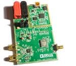
 Datasheet下载

