
 Datasheet下载
- 型号: ESDAXLC6-1BT2
- 制造商: STMicroelectronics
- 库位|库存: xxxx|xxxx
- 要求:
| 数量阶梯 | 香港交货 | 国内含税 |
| +xxxx | $xxxx | ¥xxxx |
查看当月历史价格
查看今年历史价格
ESDAXLC6-1BT2产品简介:
ICGOO电子元器件商城为您提供ESDAXLC6-1BT2由STMicroelectronics设计生产,在icgoo商城现货销售,并且可以通过原厂、代理商等渠道进行代购。 ESDAXLC6-1BT2价格参考¥0.32-¥0.42。STMicroelectronicsESDAXLC6-1BT2封装/规格:TVS - 二极管, 。您可以下载ESDAXLC6-1BT2参考资料、Datasheet数据手册功能说明书,资料中有ESDAXLC6-1BT2 详细功能的应用电路图电压和使用方法及教程。
STMicroelectronics的ESDAXLC6-1BT2是一款TVS(瞬态电压抑制)二极管,主要应用于电子设备中的静电放电(ESD)保护和瞬态过压保护。这款器件具有低电容、快速响应时间、高箝位能力和良好的重复性,适用于高速信号线和电源线的保护。

应用场景:

1. 消费电子产品:
   - 用于智能手机、平板电脑、笔记本电脑等便携式设备的USB接口、HDMI接口、耳机插孔等外部连接端口的ESD保护。这些端口容易受到外界静电干扰,ESDAXLC6-1BT2可以有效防止静电损坏内部电路。

2. 通信设备:
   - 在路由器、交换机、调制解调器等网络设备中,用于保护以太网端口、Wi-Fi模块、蓝牙模块等通信接口。这些接口在数据传输过程中可能会遇到雷击或电力波动引起的瞬态电压,ESDAXLC6-1BT2可以迅速将过压能量泄放到地,保护敏感的通信芯片。

3. 工业自动化:
   - 在工业控制系统的传感器、执行器、通信总线(如RS-485、CAN总线)等部分,提供可靠的ESD和浪涌保护。工业环境中的电磁干扰较为严重,ESDAXLC6-1BT2能够确保设备在恶劣环境下稳定运行。

4. 汽车电子:
   - 应用于车载信息娱乐系统、导航系统、倒车雷达等设备的信号线和电源线。汽车环境中存在大量的电磁干扰源,如点火系统、电动马达等,ESDAXLC6-1BT2可以保护这些设备免受瞬态电压的影响,确保行车安全。

5. 医疗设备:
   - 用于心电图机、血压计、血糖仪等便携式医疗设备的接口保护。医疗设备对可靠性和安全性要求极高,ESDAXLC6-1BT2可以有效防止静电和其他瞬态电压对设备的损害,保障患者的安全。

总之,ESDAXLC6-1BT2凭借其优异的性能和可靠性,广泛应用于各种需要ESD和瞬态过压保护的场景,特别是在高速信号传输和敏感电子设备中发挥着重要作用。
| 参数 | 数值 |
| 产品目录 | |
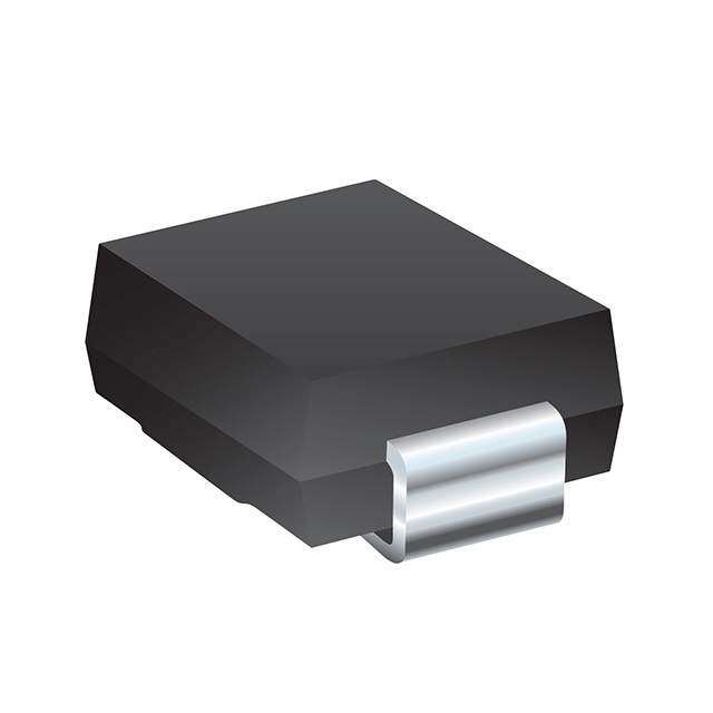
| 描述 | TVS DIODE 3VWM 17VC SOD882TTVS 二极管 - 瞬态电压抑制器 Single-Line BI ESD 0.4pF 15kV 8kV |
| 产品分类 | |
| 品牌 | STMicroelectronics |
| 产品手册 | |
| 产品图片 |
|
| rohs | 符合RoHS无铅 / 符合限制有害物质指令(RoHS)规范要求 |
| 产品系列 | 二极管与整流器,TVS二极管,TVS 二极管 - 瞬态电压抑制器,STMicroelectronics ESDAXLC6-1BT2ESDA |
| mouser_ship_limit | 该产品可能需要其他文件才能进口到中国。 |
| 数据手册 | |
| 产品型号 | ESDAXLC6-1BT2 |
| 不同频率时的电容 | 0.4pF @ 200MHz ~ 3GHz |
| 产品种类 | TVS 二极管 - 瞬态电压抑制器 |
| 供应商器件封装 | SOD-882T |
| 其它名称 | 497-13413-6 |
| 其它有关文件 | http://www.st.com/web/catalog/sense_power/FM114/CL1137/SC492/SS1421/PF254273?referrer=70071840 |
| 击穿电压 | 6 V |
| 功率-峰值脉冲 | 40W |
| 包装 | Digi-Reel® |
| 单向通道 | - |
| 双向通道 | 1 |
| 商标 | STMicroelectronics |
| 安装类型 | 表面贴装 |
| 安装风格 | SMD/SMT |
| 封装 | Reel |
| 封装/外壳 | SOD-882 |
| 峰值浪涌电流 | 1.3 A |
| 峰值脉冲功率耗散 | 40 W |
| 工作温度 | -40°C ~ 150°C (TJ) |
| 工具箱 | /product-detail/zh/Q7525688/497-8022-KIT-ND/4158065 |
| 工厂包装数量 | 12000 |
| 应用 | 通用 |
| 最大工作温度 | + 150 C |
| 最小工作温度 | - 40 C |
| 极性 | Bidirectional |
| 标准包装 | 1 |
| 电压-击穿(最小值) | 6V |
| 电压-反向关态(典型值) | 3V |
| 电压-箝位(最大值)@Ipp | 17V |
| 电流-峰值脉冲(10/1000µs) | 1A (8/20µs) |
| 电源线路保护 | 无 |
| 端接类型 | SMD/SMT |
| 类型 | 齐纳 |
| 系列 | ESDAXLC6-1BT2 |
| 钳位电压 | 3 V |


- 商务部:美国ITC正式对集成电路等产品启动337调查
- 曝三星4nm工艺存在良率问题 高通将骁龙8 Gen1或转产台积电
- 太阳诱电将投资9.5亿元在常州建新厂生产MLCC 预计2023年完工
- 英特尔发布欧洲新工厂建设计划 深化IDM 2.0 战略
- 台积电先进制程称霸业界 有大客户加持明年业绩稳了
- 达到5530亿美元!SIA预计今年全球半导体销售额将创下新高
- 英特尔拟将自动驾驶子公司Mobileye上市 估值或超500亿美元
- 三星加码芯片和SET,合并消费电子和移动部门,撤换高东真等 CEO
- 三星电子宣布重大人事变动 还合并消费电子和移动部门
- 海关总署:前11个月进口集成电路产品价值2.52万亿元 增长14.8%


PDF Datasheet 数据手册内容提取
ESDAXLC6-1BT2 Single-line bidirectional ESD protection for high speed interface Datasheet - production data Features Bidirectional device Multiple ESD strike sustainability Extra low diode capacitance: 0.4 pF Low leakage current Thin SOD882 package - 0402 size compatible Ultra small: 0.6 mm2 RoHS compliant SOD882T Complies with the following standards: ESDAXLC6-1BT2 IEC 61000-4-2 level 4 – 15 kV (air discharge) Figure 1. Functional diagram (top view) – 8 kV (contact discharge) Pin1 Applications Where transient overvoltage protection in ESD sensitive equipment is required, such as: Smartphones, mobile phone and accessories Tablets, netbooks and notebooks Portable multimedia players and accessories Digital cameras and camcorders Communication systems Description The ESDAXLC6-1BT2 is a bidirectional single line TVS diode designed to protect the data lines or other I/O ports against ESD transients. The device is ideal for applications where both reduced line capacitance and board space saving are required. August 2013 DocID023680 Rev 2 1/10 This is information on a product in full production. www.st.com
Characteristics ESDAXLC6-1BT2 1 Characteristics T able 1. Absolute maximum ratings (T = 25 °C) amb Symbol Parameter Value Unit Peak pulse voltage: V IEC 61000-4-2 contact discharge ± 16 kV PP IEC 61000-4-2 air discharge ± 25 P Peak pulse power (8/20 µs) 40 W PP I Peak pulse current (8/20 µs) 1.3 A PP T Operating junction temperature range - 40 to +150 °C j T Storage temperature range - 65 to +150 °C stg T Maximum lead temperature for soldering during 10 s 260 °C L Note: For a surge greater than the maximum values, the diode will fail in short-circuit Figure 2. Electrical characteristics (definitions) Symbol Parameter V = Breakdown voltage BR V = Stand-off voltage RM I = Leakage current @V RM RM I = Peak pulse current PP R = Dynamic impedance d αT = Voltage temperature coefficient C = Parasite capacitance Table 2. Electrical characteristics (values, T = 25 °C) amb Symbol Test condition Min. Typ. Max. Unit V I = 1 mA 6 V BR R I V = 3 V 70 nA RM RM V I = 1 A, 8/20 µA 17 V CL PP C F= (200 MHz- 3000 MHz), V = 0 V 0.4 0.5 pF line R 2/10 DocID023680 Rev 2
ESDAXLC6-1BT2 Characteristics Figure 3. Leakage current versus junction Figure 4. Junction capacitance versus applied temperature (typical values) voltage (typical values) IR(nA) C(pF) 10 0.8 0.7 0.6 1 0.5 0.4 0.3 0.1 0.2 Tj(°C) 0.1 VR(V) 0.01 0 25 50 75 100 125 150 0 1 2 3 4 5 Figure 5. ESD response to IEC 61000-4-2 Figure 6. ESD response to IEC 61000-4-2 (+8 kV contact discharge) (-8 kV contact discharge) 50V/div 50V/div 4123VVVVCCCCLLLL::::Pcccllleaaaammmkppp ciiinnnlagggm vvvpoooilllntttaaagggg eeev oaaaltttta 361g000e 0nn ssns 3-25V 4-18V 2-36V 1156V 2236V 330V 415V 1-159V 4123VVVVCCCCLLLL::::Pcccllleaaaammmkppp ciiinnnlagggm vvvpoooilllntttaaagggg eeev oaaaltttta 361g000e 0nn ssns 20 ns/div 20 ns/div Figure 7. Attenuation versus frequency S21(dB) 0.00 -1.00 dB -2.00 -3.00 -4.00 -5.00 -6.00 F(Hz) -7.00 100.0M 300.0M 1.0G 3.0G 10.0G 30.0G ESDAXLC6--1BT2 DocID023680 Rev 2 3/10 10
Package information ESDAXLC6-1BT2 2 Package information Epoxy meets UL94, V0 Lead-free package In order to meet environmental requirements, ST offers these devices in different grades of ECOPACK® packages, depending on their level of environmental compliance. ECOPACK® specifications, grade definitions and product status are available at: www.st.com. ECOPACK® is an ST trademark. Figure 8. SOD882 thin dimension definitions L1 L2 b1 b2 PIN # 1 ID e A A1 E D Table 3. SOD882 thin dimension values Dimensions Ref. Millimeters Inches Min. Typ. Max. Min. Typ. Max. A 0.30 0.40 0.012 0.016 A1 0.00 0.05 0.000 0.002 b1 0.45 0.50 0.55 0.018 0.020 0.022 b2 0.45 0.50 0.55 0.018 0.020 0.022 D 0.55 0.60 0.65 0.022 0.024 0.026 E 0.95 1.00 1.05 0.037 0.039 0.041 e 0.60 0.65 0.70 0.024 0.026 0.028 L1 0.20 0.25 0.30 0.008 0.010 0.012 L2 0.20 0.25 0.30 0.008 0.010 0.012 4/10 DocID023680 Rev 2
ESDAXLC6-1BT2 Package information Figure 9. Footprint dimension in mm (inches) 0.55 0.55 (0.022) (0.022) 0.50 0.020 0.40 (0.016) Figure 10. Marking T Pin2 Pin 1 Note: Product marking may be rotated by multiples of 180° for assembly plant differentiation. In no case should this product marking be used to orient the component for its placement on a PCB. Only pin 1 mark is to be used for this purpose. Figure 11. Tape and reel specifications Bar indicates Pin1 Ø 1.50 ± 0.1 1 2.0 ± 0.05 4.0 ± 0.1 0. ± 0.20 ± 0.2 5 7 1. 5 0. 5 0.3 / - 0.1 1.15 ± 3.5 ± 0.0 + 0 8. TywwxxzST TywwxxzST TywwxxzST TywwxxzST TywwxxzST TywwxxzST 0.70 ± 0.5 4.0 ± 0.1 0.47 ± 0.5 All dimensions are in mm User direction of unreeling DocID023680 Rev 2 5/10 10
Recommendation on PCB assembly ESDAXLC6-1BT2 3 Recommendation on PCB assembly 3.1 Stencil opening design 1. General recommendation on stencil opening design a) Stencil opening dimensions: L (Length), W (Width), T (Thickness). Figure 12. Stencil opening dimensions L T W b) General design rule Stencil thickness (T) = 75 ~ 125 µm W Aspect Ratio = -----1,5 T LW Aspect Area = ----------------------------0,66 2TL+W 2. Reference design a) Stencil opening thickness: 100 µm b) Stencil opening for central exposed pad: Opening to footprint ratio is 50%. c) Stencil opening for leads: Opening to footprint ratio is 90%. Figure 13. Recommended stencil window position Package footprint Leadfootprinton PCB 0.055 mm Leadfootprinton PCB Stencilwindow Stencilwindow position 0.39 mm position 0.45 mm 0.05 mm 0.05 mm 6/10 DocID023680 Rev 2
ESDAXLC6-1BT2 Recommendation on PCB assembly 3.2 Solder paste 1. Use halide-free flux, qualification ROL0 according to ANSI/J-STD-004. 2. “No clean” solder paste recommended. 3. Offers a high tack force to resist component displacement during PCB movement. 4. Use solder paste with fine particles: powder particle size 20-45 µm. 3.3 Placement 1. Manual positioning is not recommended. 2. It is recommended to use the lead recognition capabilities of the placement system, not the outline centering. 3. Standard tolerance of ± 0.05 mm is recommended. 4. 3.5 N placement force is recommended. Too much placement force can lead to squeezed out solder paste and cause solder joints to short. Too low placement force can lead to insufficient contact between package and solder paste that could cause open solder joints or badly centered packages. 5. To improve the package placement accuracy, a bottom side optical control should be performed with a high resolution tool. 6. For assembly, a perfect supporting of the PCB (all the more on flexible PCB) is recommended during solder paste printing, pick and place and reflow soldering by using optimized tools. 3.4 PCB design preference 1. To control the solder paste amount, the closed via is recommended instead of open vias. 2. The position of tracks and open vias in the solder area should be well balanced. The symmetrical layout is recommended, in case any tilt phenomena caused by asymmetrical solder paste amount due to the solder flow away. DocID023680 Rev 2 7/10 10
Recommendation on PCB assembly ESDAXLC6-1BT2 3.5 Reflow profile Figure 14. ST ECOPACK® recommended soldering reflow profile for PCB mounting 240-245 °C Temperature (°C) -2°C/s 250 2 - 3 °C/s 200 60sec (90max) -3°C/s 150 -6°C/s 100 0.9 °C/s 50 Time (s) 0 30 60 90 120 150 180 210 240 270 300 Note: Minimize air convection currents in the reflow oven to avoid component movement. Maximum soldering profile corresponds to the latest IPC/JEDEC J-STD-020. 8/10 DocID023680 Rev 2
ESDAXLC6-1BT2 Ordering information 4 Ordering information Figure 15. Ordering information scheme ESDA XLC 6 - 1B T2 ESDA array Extra low capacitance Breakdown voltage 6 = 6V min Direction B = Bidirectional Package T2 =Thin SOD882 (SOD882T) Table 4. Ordering information Order code Marking Package Weight Base qty Delivery mode ESDAXLC6-1BT2 T(1) SOD882T 0.8 mg 12000 Tape and reel 1. The marking can be rotated by multiples of 180° to differentiate assembly location 5 Revision history Table 5. Document revision history Date Revision Changes 04-Sep-2012 1 Initial release. 12-Aug-2013 2 Updated Figure4, Figure5, Figure6, Figure11 and Table4. DocID023680 Rev 2 9/10 10
ESDAXLC6-1BT2 Please Read Carefully: Information in this document is provided solely in connection with ST products. STMicroelectronics NV and its subsidiaries (“ST”) reserve the right to make changes, corrections, modifications or improvements, to this document, and the products and services described herein at any time, without notice. All ST products are sold pursuant to ST’s terms and conditions of sale. Purchasers are solely responsible for the choice, selection and use of the ST products and services described herein, and ST assumes no liability whatsoever relating to the choice, selection or use of the ST products and services described herein. No license, express or implied, by estoppel or otherwise, to any intellectual property rights is granted under this document. If any part of this document refers to any third party products or services it shall not be deemed a license grant by ST for the use of such third party products or services, or any intellectual property contained therein or considered as a warranty covering the use in any manner whatsoever of such third party products or services or any intellectual property contained therein. UNLESS OTHERWISE SET FORTH IN ST’S TERMS AND CONDITIONS OF SALE ST DISCLAIMS ANY EXPRESS OR IMPLIED WARRANTY WITH RESPECT TO THE USE AND/OR SALE OF ST PRODUCTS INCLUDING WITHOUT LIMITATION IMPLIED WARRANTIES OF MERCHANTABILITY, FITNESS FOR A PARTICULAR PURPOSE (AND THEIR EQUIVALENTS UNDER THE LAWS OF ANY JURISDICTION), OR INFRINGEMENT OF ANY PATENT, COPYRIGHT OR OTHER INTELLECTUAL PROPERTY RIGHT. ST PRODUCTS ARE NOT AUTHORIZED FOR USE IN WEAPONS. NOR ARE ST PRODUCTS DESIGNED OR AUTHORIZED FOR USE IN: (A) SAFETY CRITICAL APPLICATIONS SUCH AS LIFE SUPPORTING, ACTIVE IMPLANTED DEVICES OR SYSTEMS WITH PRODUCT FUNCTIONAL SAFETY REQUIREMENTS; (B) AERONAUTIC APPLICATIONS; (C) AUTOMOTIVE APPLICATIONS OR ENVIRONMENTS, AND/OR (D) AEROSPACE APPLICATIONS OR ENVIRONMENTS. WHERE ST PRODUCTS ARE NOT DESIGNED FOR SUCH USE, THE PURCHASER SHALL USE PRODUCTS AT PURCHASER’S SOLE RISK, EVEN IF ST HAS BEEN INFORMED IN WRITING OF SUCH USAGE, UNLESS A PRODUCT IS EXPRESSLY DESIGNATED BY ST AS BEING INTENDED FOR “AUTOMOTIVE, AUTOMOTIVE SAFETY OR MEDICAL” INDUSTRY DOMAINS ACCORDING TO ST PRODUCT DESIGN SPECIFICATIONS. PRODUCTS FORMALLY ESCC, QML OR JAN QUALIFIED ARE DEEMED SUITABLE FOR USE IN AEROSPACE BY THE CORRESPONDING GOVERNMENTAL AGENCY. Resale of ST products with provisions different from the statements and/or technical features set forth in this document shall immediately void any warranty granted by ST for the ST product or service described herein and shall not create or extend in any manner whatsoever, any liability of ST. ST and the ST logo are trademarks or registered trademarks of ST in various countries. Information in this document supersedes and replaces all information previously supplied. The ST logo is a registered trademark of STMicroelectronics. All other names are the property of their respective owners. © 2013 STMicroelectronics - All rights reserved STMicroelectronics group of companies Australia - Belgium - Brazil - Canada - China - Czech Republic - Finland - France - Germany - Hong Kong - India - Israel - Italy - Japan - Malaysia - Malta - Morocco - Philippines - Singapore - Spain - Sweden - Switzerland - United Kingdom - United States of America www.st.com 10/10 DocID023680 Rev 2