ICGOO在线商城 > ERZ-VF2T101
 Datasheet下载
- 型号: ERZ-VF2T101
- 制造商: Panasonic Corporation
- 库位|库存: xxxx|xxxx
- 要求:
| 数量阶梯 | 香港交货 | 国内含税 |
| +xxxx | $xxxx | ¥xxxx |
查看当月历史价格
查看今年历史价格
ERZ-VF2T101产品简介:
ICGOO电子元器件商城为您提供ERZ-VF2T101由Panasonic Corporation设计生产,在icgoo商城现货销售,并且可以通过原厂、代理商等渠道进行代购。 提供ERZ-VF2T101价格参考以及Panasonic CorporationERZ-VF2T101封装/规格参数等产品信息。 你可以下载ERZ-VF2T101参考资料、Datasheet数据手册功能说明书, 资料中有ERZ-VF2T101详细功能的应用电路图电压和使用方法及教程。
| 参数 | 数值 |
| 产品目录 | |
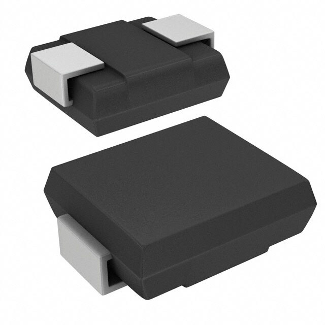
| 描述 | VARISTOR 90V 400A 2-SMD J-LEAD |
| 产品分类 | |
| 品牌 | Panasonic Electronic Components |
| 数据手册 | |
| 产品图片 | |
| 产品型号 | ERZ-VF2T101 |
| rohs | 无铅 / 符合限制有害物质指令(RoHS)规范要求 |
| 产品系列 | ZNR® |
| 产品目录绘图 |
|
| 产品目录页面 | |
| 其它名称 | P7333CT |
| 包装 | 剪切带 (CT) |
| 变阻器电压 | 90V |
| 封装/外壳 | 2-SMD,J 形引线 |
| 最大AC电压 | 60VAC |
| 最大DC电压 | 85VDC |
| 标准包装 | 1 |
| 电流-浪涌 | 400A |
| 电路数 | 1 |
| 能量 | 2.0J |


- 商务部:美国ITC正式对集成电路等产品启动337调查
- 曝三星4nm工艺存在良率问题 高通将骁龙8 Gen1或转产台积电
- 太阳诱电将投资9.5亿元在常州建新厂生产MLCC 预计2023年完工
- 英特尔发布欧洲新工厂建设计划 深化IDM 2.0 战略
- 台积电先进制程称霸业界 有大客户加持明年业绩稳了
- 达到5530亿美元!SIA预计今年全球半导体销售额将创下新高
- 英特尔拟将自动驾驶子公司Mobileye上市 估值或超500亿美元
- 三星加码芯片和SET,合并消费电子和移动部门,撤换高东真等 CEO
- 三星电子宣布重大人事变动 还合并消费电子和移动部门
- 海关总署:前11个月进口集成电路产品价值2.52万亿元 增长14.8%


PDF Datasheet 数据手册内容提取
“ZNR” Surge Absorbers (Type SMD) “ZNR” Surge Absorbers Type: SMD Series: VF Features ● Large withstanding surge current capability, in compact size ● Designed for fl ow/refl ow solderings ● Low clamping voltage ● RoHS compliant Recommended Applications ● Protection of communication modules (Modem, xDSL, Terminal Adopter) ● Protection of consumer, industrial equipment ● Absorption of switching surge from relays Applicable Standards ● PCQC (GB/T10193, GB/T10194) Registered in "Panasonic Part No." ■ As for Handling Precautions and Minimum Quantity / Packing Unit Please see Related Information Explanation of Part Numbers 1 2 3 4 5 6 7 8 9 10 11 12 E R Z V F M Product Code Series Construction Nominal Design No. Varistor Voltage Packaging Style 1 Bulk 2 Taping Construction 2 4 1 ZNR element ZnO etc. 3 2 Resin mold Epoxy Resin(UL94V-0 approved) 1 3 Conductive Silver adhesive 4 Electrode Silver 5 Lead terminals Sn plated Ni-Fe Alloy 5 Dimensions in mm (not to scale) Unit : mm Part No. W L H S E H ERZVF□M□□□ 6.0±0.4 8.0±0.5 3.2±0.3 1.3±0.3 2.5±0.2 S S E L W Design and specifications are each subject to change without notice. Ask factory for the current technical specifications before purchase and/or use. Should a safety concern arise regarding this product, please be sure to contact us immediately. 03 Jan. 2015
“ZNR” Surge Absorbers (Type SMD) Ratings and Characteristics ● Operating Temperature Range : –40 to 85 °C ● Storage Temperature Range : –40 to 125 °C Maximum Clamping Maximum MaximumPeak Varistor Rated Allowable Voltage at Ip Energy Current Voltage Power Part No. Voltage (max.) (2 ms) (8/20 μs, 2 times) Measuring V (V) ACrms (V) DC (V) (V) (W) (J) (A) 1 mA Current (A) ERZVF□M220 22(20 to 24) 14 18 43 2.5 0.02 0.9 125 ERZVF□M270 27(24 to 30) 17 22 53 2.5 0.02 1.0 125 ERZVF□M330 33(30 to 36) 20 26 65 2.5 0.02 1.2 125 ERZVF□M390 39(35 to 43) 25 31 77 2.5 0.02 1.5 125 ERZVF□M470 47(42 to 52) 30 38 93 2.5 0.02 1.8 125 ERZVF□M560 56(50 to 62) 35 45 110 2.5 0.02 2.2 125 ERZVF□M680 68(61 to 75) 40 56 135 2.5 0.02 2.5 125 ERZVF□M820 82(74 to 90) 50 65 135 10 0.25 3.5 600 M ERZVF□M101 100(90 to 110) 60 85 165 10 0.25 4.0 600 □ F ERZVF□M121 120(108 to 132) 75 100 200 10 0.25 5.0 600 V e ERZVF□M151 150(135 to 165) 95 125 250 10 0.25 6.0 600 p Ty ERZVF□M201 200(185 to 225) 130 170 340 10 0.25 8.0 600 ERZVF□M221 220(198 to 242) 140 180 360 10 0.25 9.0 600 ERZVF□M241 240(216 to 264) 150 200 395 10 0.25 10.0 600 ERZVF□M271 270(247 to 303) 175 225 455 10 0.25 12.0 600 ERZVF□M331 330(297 to 363) 210 270 545 10 0.1 8.0 300 ERZVF□M361 360(324 to 396) 230 300 595 10 0.1 9.0 300 ERZVF□M391 390(351 to 429) 250 320 650 10 0.1 9.0 300 ERZVF□M431 430(387 to 473) 275 350 710 10 0.1 10.0 300 ERZVF□M471 470(423 to 517) 300 385 775 10 0.1 10.0 300 Packaging Style Code: “1” for bulk, “2” for embossed taping Design and specifications are each subject to change without notice. Ask factory for the current technical specifications before purchase and/or use. Should a safety concern arise regarding this product, please be sure to contact us immediately. 02 Jan. 2015
“ZNR” Surge Absorbers (Type SMD) Typical Characteristics Voltage vs. Current Impulse Derating (Relation between impulse width and impulse current multiple) ERZVF1(2)M220 to ERZVF1(2)M680 ERZVF1(2)M220 to ERZVF1(2)M680 Max. Max. Clamping Voltage 300 2 times : 5 min. interval 400 Leakage Current 200 up to 10 times : 2 min. interval 3210009800000 654332286793720000000 nt (A)11234503450000001110001112 0006T3 2TTiT54m iiiTTTmmmeiiimmmeeseussseeepsss to 106 times :10 sec. interval 7600 urre 2 C e (V) 5400 6 8 0 pulse 0.51 Voltag 30 54 67 00 Im 000...234 20 0.1 270 2 2 0 20 100 1000 10000 10 Impulse Width (μs) 98 390 Test Current Waveform ERZVF1(2)M820 to ERZVF1(2)M271 7 330 10–6 to 10–3A: Direct Current 2000 6 10–1 to 103 A: 8/20 μs 2 times : 5 min. interval 1000 up to 10 times : 2 min. interval 5 500 up to 106 times :10 sec. interval 4 340000 2 Ti ERZV3F101–6(2)M1802–50 to 1E0–R4ZVF101–(32)M4107–12 Cur1r0e–n1t (A) 100 101 102 103 104 mpulse Current (A)12123450000000001111000054131 TT 2T00Tii immiTmm6 iTemeeemsismsesesses I 5 4 3 Max. Max. Clamping Voltage 2 Leakage Current 2000 1 471 0.1 1098000000 433911 433396111 E2R0ZVF1(21)0M0I3m3p1u lstoe WEiRd1thZ0 0V(μ0Fs)1(2)M47110000 700 271 600 241 1000 221 2 times : 5 min. interval 500 201 up to 10 times : 2 min. interval 400 151 up to 106 times :10 sec. interval Voltage (V)32100090000 422170751111361 181022101 mpulse Current (A)1010011111010000054 36 2 T2 TTTTT iiiTimimimmmmimeeeeeseessssss 80 1 2 1 I 7600 1 0 1 1 50 8 2 0 Test Current Waveform 40 224211 1100––61 ttoo 1100–43 A A : :8 D/2ir0e cμts Current 30 0.1 10–6 10–5 10–4 10–3 10–2 10–1 100 101 102 103 104 20 100 1000 10000 Current (A) Impulse Width (μs) Design and specifications are each subject to change without notice. Ask factory for the current technical specifications before purchase and/or use. Should a safety concern arise regarding this product, please be sure to contact us immediately. 02 Jan. 2015
“ZNR” Surge Absorbers (Type SMD) Marking Contents 1 1 Product Name ZNR, ZNR Surge Absorbers Z N R 2 Series VF□M, VF Series V F M 2 01 3 3 Abbreviation of The fi rst two digits are signifi cant fi gures and the third one 4 Part No. denotes the number of zeros following. ✽ Left (Year) 2011:1, 2012:2, 2013:3, 2014:4, 2015:5, 2016:6 4 Date Code Right(Month) Jan. to Sep.:1 to 9, Oct.:O, Nov.:N, Dec.:D ✽ If the 10's digit of a Christian year is an even year, as an end abbreviation, an alphabetic character is used. 1 : A, 2 : B, 3 : C, 4 : D, 5 : E, 6 : F, 7 : G, 8 : H, 9 : J, 0 : K If the 10's digit of a Christian year is an odd year, as an end abbreviation, a number is used. Packaging Methods ● Packing Quantity Style Quantity Embossed taping 2,000 pcs./reel Bulk 200 pcs./bag ● Reel ● Embossed Taping T (W=16 mm) E t1 Feeding hole Chip pocket C f D0 P2P0 E A B F r D B W t2 P1 Chip component Tape running direction A W t (not to scale) (not to scale) Part No. A B C D E Part No. A B W F E P 1 ERZVF□M□□□ 382 max. 50 min. 13.0±0.5 21.0±0.8 2.0±0.5 ERZVF□M□□□ 6.8±0.2 11.9 max. 16.0±0.3 7.5±0.10 1.75±0.10 8.0±0.1 Part No. W T t r Part No. P P fD t t 2 0 0 1 2 ERZVF□M□□□ 16.4+2.0 22.4 max. 2.5±0.5 1.0 ERZVF□M□□□ 2.0±0.1 4.0±0.1 1.5+0.1 0.6 max. 6.5 max. 0 0 Design and specifications are each subject to change without notice. Ask factory for the current technical specifications before purchase and/or use. Should a safety concern arise regarding this product, please be sure to contact us immediately. 02 Jan. 2015
“ZNR” Surge Absorbers (Type SMD) Performance Characteristics Characteristics Test Methods Specifi cations Standard Test Electrical measurements (initial/after tests) shall be conducted at ——— Condition temperature of 5 to 35 °C, relative humidity of maximum 85 % The voltage between two terminals with the specifi ed measuring Varistor Voltage current 1mA DC applied is called V1 or V1mA. The measurement should be made as fast as possible to avoid heat effects. Maximum Allowable The recommended maximum sinusoidal wave voltage (rms) or Voltage the maximum DC voltage that can be applied continuously. The maximum voltage between two terminals with the specifi ed Clamping Voltage impulse current (8/20 μs). To meet the specifi ed value. The maximum power that can be applied within the specified Rated Power ambient temperature. Maximum energy of less than ±10 % of the varistor voltage Maximum Energy change when the standard impulse (2 ms) is applied one time. Maximum current of less than ±10 % of the varistor voltage change Maximum when impulse current (8/20 μs) is applied twice continuously with an Peak Current interval of 5 minutes. Temperature Co ef fi cient V1mA at 85 °C – V1mA at 25 °C × 1 × 100(%/°C) 0 to –0.05 %/°C of Varistor Volta ge V1mA at 25 °C 60 The change of Vc shall be measured after the specifi ed impulse is applied 10000 times continuously with an interval of 10 seconds at room temperature. Impulse Life (I) Part No. Waveform Current ΔV1mA/V1mA < ±10 % ERZVF□M220 to ERZVF□M680 8/20 μs 18 A ERZVF□M820 to ERZVF□M271 8/20 μs 50 A ERZVF□M331 to ERZVF□M471 8/20 μs 30 A The change of Vc shall be measured after the specifi ed impulse is applied 100000 times continuously with an interval of 10 seconds at room temperature. Impulse Life (II) Part No. Waveform Current ΔV1mA/V1mA < ±10 % ERZVF□M220 to ERZVF□M680 8/20 μs 12 A ERZVF□M820 to ERZVF□M271 8/20 μs 35 A ERZVF□M331 to ERZVF□M471 8/20 μs 20 A Recommendation Land Size Land 8.0 Product 0 0 6. 3. Occupied Space 5.0 10.0 Unit : mm Design and specifications are each subject to change without notice. Ask factory for the current technical specifications before purchase and/or use. Should a safety concern arise regarding this product, please be sure to contact us immediately. 03 Jan. 2015