ICGOO在线商城 > 集成电路(IC) > 嵌入式 - FPGA(现场可编程门阵列) > EPF10K20RC240-3
 Datasheet下载
- 型号: EPF10K20RC240-3
- 制造商: altera
- 库位|库存: xxxx|xxxx
- 要求:
| 数量阶梯 | 香港交货 | 国内含税 |
| +xxxx | $xxxx | ¥xxxx |
查看当月历史价格
查看今年历史价格
EPF10K20RC240-3产品简介:
ICGOO电子元器件商城为您提供EPF10K20RC240-3由altera设计生产,在icgoo商城现货销售,并且可以通过原厂、代理商等渠道进行代购。 EPF10K20RC240-3价格参考¥3959.40-¥5015.30。alteraEPF10K20RC240-3封装/规格:嵌入式 - FPGA(现场可编程门阵列), 。您可以下载EPF10K20RC240-3参考资料、Datasheet数据手册功能说明书,资料中有EPF10K20RC240-3 详细功能的应用电路图电压和使用方法及教程。
| 参数 | 数值 |
| 产品目录 | 集成电路 (IC) |
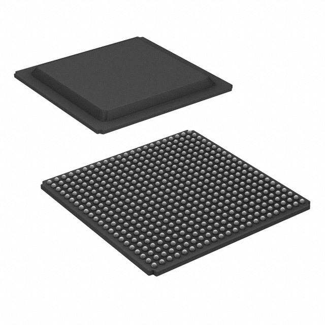
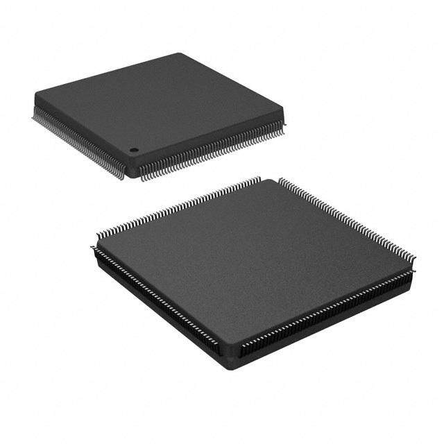
| 描述 | IC FPGA 189 I/O 240RQFP |
| 产品分类 | |
| I/O数 | 189 |
| LAB/CLB数 | 144 |
| 品牌 | Altera |
| 数据手册 | 点击此处下载产品Datasheethttp://www.altera.com/literature/ds/pkgds.pdf#page=87-88 |
| 产品图片 |
|
| 产品型号 | EPF10K20RC240-3 |
| PCN封装 | |
| rohs | 含铅 / 不符合限制有害物质指令(RoHS)规范要求 |
| 产品系列 | FLEX-10K® |
| 产品培训模块 | http://www.digikey.cn/PTM/IndividualPTM.page?site=cn&lang=zhs&ptm=25450 |
| 产品目录页面 | |
| 供应商器件封装 | 240-RQFP(32x32) |
| 其它名称 | 544-2211 |
| 安装类型 | 表面贴装 |
| 封装/外壳 | 240-BFQFP 裸露焊盘 |
| 工作温度 | 0°C ~ 70°C |
| 总RAM位数 | 12288 |
| 栅极数 | 63000 |
| 标准包装 | 24 |
| 电压-电源 | 4.75 V ~ 5.25 V |
| 逻辑元件/单元数 | 1152 |


- 商务部:美国ITC正式对集成电路等产品启动337调查
- 曝三星4nm工艺存在良率问题 高通将骁龙8 Gen1或转产台积电
- 太阳诱电将投资9.5亿元在常州建新厂生产MLCC 预计2023年完工
- 英特尔发布欧洲新工厂建设计划 深化IDM 2.0 战略
- 台积电先进制程称霸业界 有大客户加持明年业绩稳了
- 达到5530亿美元!SIA预计今年全球半导体销售额将创下新高
- 英特尔拟将自动驾驶子公司Mobileye上市 估值或超500亿美元
- 三星加码芯片和SET,合并消费电子和移动部门,撤换高东真等 CEO
- 三星电子宣布重大人事变动 还合并消费电子和移动部门
- 海关总署:前11个月进口集成电路产品价值2.52万亿元 增长14.8%


PDF Datasheet 数据手册内容提取
Includes FLEX 10KA FLEX 10K Embedded Programmable ® Logic Device Family January 2003, ver. 4.2 Data Sheet Features... ■ The industry’s first embedded programmable logic device (PLD) family, providing System-on-a-Programmable-Chip (SOPC) integration – Embedded array for implementing megafunctions, such as efficient memory and specialized logic functions – Logic array for general logic functions ■ High density – 10,000 to 250,000 typical gates (see Tables1 and 2) – Up to 40,960 RAM bits; 2,048 bits per embedded array block (EAB), all of which can be used without reducing logic capacity ■ System-level features – MultiVoltTM I/O interface support – 5.0-V tolerant input pins in FLEX® 10KA devices – Low power consumption (typical specification less than 0.5 mA in standby mode for most devices) – FLEX 10K and FLEX 10KA devices support peripheral component interconnect Special Interest Group (PCI SIG) PCI Local Bus Specification, Revision 2.2 – FLEX 10KA devices include pull-up clamping diode, selectable on a pin-by-pin basis for 3.3-V PCI compliance – Select FLEX 10KA devices support 5.0-V PCI buses with eight or fewer loads – Built-in Joint Test Action Group (JTAG) boundary-scan test (BST) circuitry compliant with IEEE Std. 1149.1-1990, available without consuming any device logic Table 1.FLEX 10K Device Features Feature EPF10K10 EPF10K20 EPF10K30 EPF10K40 EPF10K50 EPF10K10A EPF10K30A EPF10K50V Typical gates (logic and RAM) (1) 10,000 20,000 30,000 40,000 50,000 Maximum system gates 31,000 63,000 69,000 93,000 116,000 Logic elements (LEs) 576 1,152 1,728 2,304 2,880 Logic array blocks (LABs) 72 144 216 288 360 Embedded array blocks (EABs) 3 6 6 8 10 Total RAM bits 6,144 12,288 12,288 16,384 20,480 Maximum user I/O pins 150 189 246 189 310 Altera Corporation 1 DS-F10K-4.2
FLEX 10K Embedded Programmable Logic Device Family Data Sheet Table 2.FLEX 10K Device Features Feature EPF10K70 EPF10K100 EPF10K130V EPF10K250A EPF10K100A Typical gates (logic and 70,000 100,000 130,000 250,000 RAM) (1) Maximum system gates 118,000 158,000 211,000 310,000 LEs 3,744 4,992 6,656 12,160 LABs 468 624 832 1,520 EABs 9 12 16 20 Total RAM bits 18,432 24,576 32,768 40,960 Maximum user I/O pins 358 406 470 470 Note to tables: (1) The embedded IEEE Std. 1149.1 JTAG circuitry adds up to 31,250 gates in addition to the listed typical or maximum system gates. ...and More – Devices are fabricated on advanced processes and operate with a 3.3-V or 5.0-V supply voltage (see Table3 Features – In-circuit reconfigurability (ICR) via external configuration device, intelligent controller, or JTAG port – ClockLockTM and ClockBoostTM options for reduced clock delay/skew and clock multiplication – Built-in low-skew clock distribution trees – 100% functional testing of all devices; test vectors or scan chains are not required Table 3.Supply Voltages for FLEX 10K & FLEX 10KA Devices 5.0-V Devices 3.3-V Devices EPF10K10 EPF10K10A EPF10K20 EPF10K30A EPF10K30 EPF10K50V EPF10K40 EPF10K100A EPF10K50 EPF10K130V EPF10K70 EPF10K250A EPF10K100 2 Altera Corporation
FLEX 10K Embedded Programmable Logic Device Family Data Sheet ■ Flexible interconnect – FastTrack® Interconnect continuous routing structure for fast, predictable interconnect delays – Dedicated carry chain that implements arithmetic functions such as fast adders, counters, and comparators (automatically used by software tools and megafunctions) – Dedicated cascade chain that implements high-speed, high-fan-in logic functions (automatically used by software tools and megafunctions) – Tri-state emulation that implements internal tri-state buses – Up to six global clock signals and four global clear signals ■ Powerful I/O pins – Individual tri-state output enable control for each pin – Open-drain option on each I/O pin – Programmable output slew-rate control to reduce switching noise – FLEX 10KA devices support hot-socketing ■ Peripheral register for fast setup and clock-to-output delay ■ Flexible package options – Available in a variety of packages with 84 to 600 pins (see Tables4 and 5) – Pin-compatibility with other FLEX10K devices in the same package – FineLine BGATM packages maximize board space efficiency ■ Software design support and automatic place-and-route provided by Altera development systems for Windows-based PCs and Sun SPARCstation, HP 9000 Series 700/800 workstations ■ Additional design entry and simulation support provided by EDIF 2 0 0 and 3 0 0 netlist files, library of parameterized modules (LPM), DesignWare components, Verilog HDL, VHDL, and other interfaces to popular EDA tools from manufacturers such as Cadence, Exemplar Logic, Mentor Graphics, OrCAD, Synopsys, Synplicity, VeriBest, and Viewlogic Altera Corporation 3
FLEX 10K Embedded Programmable Logic Device Family Data Sheet Table 4.FLEX10K Package Options & I/O Pin Count Note (1) Device 84-Pin 100-Pin 144-Pin TQFP 208-Pin 240-Pin PLCC TQFP PQFP PQFP RQFP RQFP EPF10K10 59 102 134 EPF10K10A 66 102 134 EPF10K20 102 147 189 EPF10K30 147 189 EPF10K30A 102 147 189 EPF10K40 147 189 EPF10K50 189 EPF10K50V 189 EPF10K70 189 EPF10K100 EPF10K100A 189 EPF10K130V EPF10K250A Table 5.FLEX10K Package Options & I/O Pin Count (Continued) Note (1) Device 503-Pin 599-Pin 256-Pin 356-Pin 484-Pin 600-Pin 403-Pin PGA PGA FineLine BGA BGA FineLine BGA BGA PGA EPF10K10 EPF10K10A 150 150 (2) EPF10K20 EPF10K30 246 EPF10K30A 191 246 246 EPF10K40 EPF10K50 274 310 EPF10K50V 274 EPF10K70 358 EPF10K100 406 EPF10K100A 274 369 406 EPF10K130V 470 470 EPF10K250A 470 470 4 Altera Corporation
FLEX 10K Embedded Programmable Logic Device Family Data Sheet Notes to tables: (1) FLEX 10K and FLEX 10KA device package types include plastic J-lead chip carrier (PLCC), thin quad flat pack (TQFP), plastic quad flat pack (PQFP), power quad flat pack (RQFP), ball-grid array (BGA), pin-grid array (PGA), and FineLine BGATM packages. (2) This option is supported with a 256-pin FineLine BGA package. By using SameFrame pin migration, all FineLine BGA packages are pin compatible. For example, a board can be designed to support both 256-pin and 484-pin FineLine BGA packages. The Altera software automatically avoids conflicting pins when future migration is set. General Altera’s FLEX10K devices are the industry’s first embedded PLDs. Based on reconfigurable CMOS SRAM elements, the Flexible Logic Element Description MatriX (FLEX) architecture incorporates all features necessary to implement common gate array megafunctions. With up to 250,000 gates, the FLEX10K family provides the density, speed, and features to integrate entire systems, including multiple 32-bit buses, into a single device. FLEX 10K devices are reconfigurable, which allows 100% testing prior to shipment. As a result, the designer is not required to generate test vectors for fault coverage purposes. Additionally, the designer does not need to manage inventories of different ASIC designs; FLEX 10K devices can be configured on the board for the specific functionality required. Table6 shows FLEX 10K performance for some common designs. All performance values were obtained with Synopsys DesignWare or LPM functions. No special design technique was required to implement the applications; the designer simply inferred or instantiated a function in a Verilog HDL, VHDL, Altera Hardware Description Language (AHDL), or schematic design file. Table 6.FLEX10K & FLEX 10KA Performance Application Resources Performance Units Used LEs EABs -1 Speed -2 Speed -3 Speed -4 Speed Grade Grade Grade Grade 16-bit loadable 16 0 204 166 125 95 MHz counter (1) 16-bit accumulator (1) 16 0 204 166 125 95 MHz 16-to-1 multiplexer (2) 10 0 4.2 5.8 6.0 7.0 ns 256 × 8 RAM read 0 1 172 145 108 84 MHz cycle speed (3) 256 × 8 RAM write 0 1 106 89 68 63 MHz cycle speed (3) Notes: (1) The speed grade of this application is limited because of clock high and low specifications. (2) This application uses combinatorial inputs and outputs. (3) This application uses registered inputs and outputs. Altera Corporation 5
FLEX 10K Embedded Programmable Logic Device Family Data Sheet The FLEX10K architecture is similar to that of embedded gate arrays, the fastest-growing segment of the gate array market. As with standard gate arrays, embedded gate arrays implement general logic in a conventional “sea-of-gates” architecture. In addition, embedded gate arrays have dedicated die areas for implementing large, specialized functions. By embedding functions in silicon, embedded gate arrays provide reduced die area and increased speed compared to standard gate arrays. However, embedded megafunctions typically cannot be customized, limiting the designer’s options. In contrast, FLEX10K devices are programmable, providing the designer with full control over embedded megafunctions and general logic while facilitating iterative design changes during debugging. Each FLEX10K device contains an embedded array and a logic array. The embedded array is used to implement a variety of memory functions or complex logic functions, such as digital signal processing (DSP), microcontroller, wide-data-path manipulation, and data-transformation functions. The logic array performs the same function as the sea-of-gates in the gate array: it is used to implement general logic, such as counters, adders, state machines, and multiplexers. The combination of embedded and logic arrays provides the high performance and high density of embedded gate arrays, enabling designers to implement an entire system on a single device. FLEX10K devices are configured at system power-up with data stored in an Altera serial configuration device or provided by a system controller. Altera offers the EPC1, EPC2, EPC16, and EPC1441 configuration devices, which configure FLEX10K devices via a serial data stream. Configuration data can also be downloaded from system RAM or from Altera’s BitBlasterTM serial download cable or ByteBlasterMVTM parallel port download cable. After a FLEX10K device has been configured, it can be reconfigured in-circuit by resetting the device and loading new data. Because reconfiguration requires less than 320ms, real-time changes can be made during system operation. FLEX 10K devices contain an optimized interface that permits microprocessors to configure FLEX 10K devices serially or in parallel, and synchronously or asynchronously. The interface also enables microprocessors to treat a FLEX 10K device as memory and configure the device by writing to a virtual memory location, making it very easy for the designer to reconfigure the device. 6 Altera Corporation
FLEX 10K Embedded Programmable Logic Device Family Data Sheet f For more information, see the following documents: ■ Configuration Devices for APEX & FLEX Devices Data Sheet ■ BitBlaster Serial Download Cable Data Sheet ■ ByteBlasterMV Parallel Port Download Cable Data Sheet ■ Application Note116 (Configuring APEX 20K, FLEX 10K & FLEX 6000 Devices) FLEX10K devices are supported by Altera development systems; single, integrated packages that offer schematic, text (including AHDL), and waveform design entry, compilation and logic synthesis, full simulation and worst-case timing analysis, and device configuration. The Altera software provides EDIF200 and 300, LPM, VHDL, Verilog HDL, and other interfaces for additional design entry and simulation support from other industry-standard PC- and UNIX workstation-based EDA tools. The Altera software works easily with common gate array EDA tools for synthesis and simulation. For example, the Altera software can generate Verilog HDL files for simulation with tools such as Cadence Verilog-XL. Additionally, the Altera software contains EDA libraries that use device- specific features such as carry chains which are used for fast counter and arithmetic functions. For instance, the Synopsys Design Compiler library supplied with the Altera development systems include DesignWare functions that are optimized for the FLEX 10K architecture. The Altera development systems run on Windows-based PCs and Sun SPARCstation, and HP 9000 Series 700/800 workstations. f See the MAX+PLUSII Programmable Logic Development System & Software Data Sheet for more information. Functional Each FLEX10K device contains an embedded array to implement memory and specialized logic functions, and a logic array to implement Description general logic. The embedded array consists of a series of EABs. When implementing memory functions, each EAB provides 2,048 bits, which can be used to create RAM, ROM, dual-port RAM, or first-in first-out (FIFO) functions. When implementing logic, each EAB can contribute 100 to 600 gates towards complex logic functions, such as multipliers, microcontrollers, state machines, and DSP functions. EABs can be used independently, or multiple EABs can be combined to implement larger functions. Altera Corporation 7
FLEX 10K Embedded Programmable Logic Device Family Data Sheet The logic array consists of logic array blocks (LABs). Each LAB contains eight LEs and a local interconnect. An LE consists of a 4-input look-up table (LUT), a programmable flipflop, and dedicated signal paths for carry and cascade functions. The eight LEs can be used to create medium-sized blocks of logic—8-bit counters, address decoders, or state machines—or combined across LABs to create larger logic blocks. Each LAB represents about 96 usable gates of logic. Signal interconnections within FLEX10K devices and to and from device pins are provided by the FastTrack Interconnect, a series of fast, continuous row and column channels that run the entire length and width of the device. Each I/O pin is fed by an I/O element (IOE) located at the end of each row and column of the FastTrack Interconnect. Each IOE contains a bidirectional I/O buffer and a flipflop that can be used as either an output or input register to feed input, output, or bidirectional signals. When used with a dedicated clock pin, these registers provide exceptional performance. As inputs, they provide setup times as low as 1.6ns and hold times of 0ns; as outputs, these registers provide clock-to-output times as low as 5.3ns. IOEs provide a variety of features, such as JTAG BST support, slew-rate control, tri-state buffers, and open-drain outputs. Figure1 shows a block diagram of the FLEX10K architecture. Each group of LEs is combined into an LAB; LABs are arranged into rows and columns. Each row also contains a single EAB. The LABs and EABs are interconnected by the FastTrack Interconnect. IOEs are located at the end of each row and column of the FastTrack Interconnect. 8 Altera Corporation
FLEX 10K Embedded Programmable Logic Device Family Data Sheet Figure 1. FLEX10K Device Block Diagram Embedded Array Block (EAB) I/O Element IOE IOE IOE IOE IOE IOE IOE IOE IOE IOE (IOE) IOE IOE IOE IOE Column Logic Array Interconnect EAB Logic Array Block (LAB) IOE IOE IOE IOE Logic Element (LE) Row Interconnect EAB Local Interconnect Logic Array IOE IOE IOE IOE IOE IOE IOE IOE IOE IOE Embedded Array FLEX10K devices provide six dedicated inputs that drive the flipflops’ control inputs to ensure the efficient distribution of high-speed, low-skew (less than 1.5 ns) control signals. These signals use dedicated routing channels that provide shorter delays and lower skews than the FastTrack Interconnect. Four of the dedicated inputs drive four global signals. These four global signals can also be driven by internal logic, providing an ideal solution for a clock divider or an internally generated asynchronous clear signal that clears many registers in the device. Embedded Array Block The EAB is a flexible block of RAM with registers on the input and output ports, and is used to implement common gate array megafunctions. The EAB is also suitable for functions such as multipliers, vector scalars, and error correction circuits, because it is large and flexible. These functions can be combined in applications such as digital filters and microcontrollers. Altera Corporation 9
FLEX 10K Embedded Programmable Logic Device Family Data Sheet Logic functions are implemented by programming the EAB with a read- only pattern during configuration, creating a large LUT. With LUTs, combinatorial functions are implemented by looking up the results, rather than by computing them. This implementation of combinatorial functions can be faster than using algorithms implemented in general logic, a performance advantage that is further enhanced by the fast access times of EABs. The large capacity of EABs enables designers to implement complex functions in one logic level without the routing delays associated with linked LEs or field-programmable gate array (FPGA) RAM blocks. For example, a single EAB can implement a 4 × 4 multiplier with eight inputs and eight outputs. Parameterized functions such as LPM functions can automatically take advantage of the EAB. The EAB provides advantages over FPGAs, which implement on-board RAM as arrays of small, distributed RAM blocks. These FPGA RAM blocks contain delays that are less predictable as the size of the RAM increases. In addition, FPGA RAM blocks are prone to routing problems because small blocks of RAM must be connected together to make larger blocks. In contrast, EABs can be used to implement large, dedicated blocks of RAM that eliminate these timing and routing concerns. EABs can be used to implement synchronous RAM, which is easier to use than asynchronous RAM. A circuit using asynchronous RAM must generate the RAM write enable (WE) signal, while ensuring that its data and address signals meet setup and hold time specifications relative to the WE signal. In contrast, the EAB’s synchronous RAM generates its own WE signal and is self-timed with respect to the global clock. A circuit using the EAB’s self-timed RAM need only meet the setup and hold time specifications of the global clock. When used as RAM, each EAB can be configured in any of the following sizes: 256×8, 512×4, 1,024×2, or 2,048×1. See Figure2. Figure 2. EAB Memory Configurations 256 × 8 512 × 4 1,024 × 2 2,048 × 1 10 Altera Corporation
FLEX 10K Embedded Programmable Logic Device Family Data Sheet Larger blocks of RAM are created by combining multiple EABs. For example, two 256× 8 RAM blocks can be combined to form a 256×16RAM block; two 512×4 blocks of RAM can be combined to form a 512×8RAM block. See Figure3. Figure 3. Examples of Combining EABs 256 × 16 512 × 8 256 × 8 512 × 4 256 × 8 512 × 4 If necessary, all EABs in a device can be cascaded to form a single RAM block. EABs can be cascaded to form RAM blocks of up to 2,048words without impacting timing. Altera’s software automatically combines EABs to meet a designer’s RAM specifications. EABs provide flexible options for driving and controlling clock signals. Different clocks can be used for the EAB inputs and outputs. Registers can be independently inserted on the data input, EAB output, or the address and WE inputs. The global signals and the EAB local interconnect can drive the WE signal. The global signals, dedicated clock pins, and EAB local interconnect can drive the EAB clock signals. Because the LEs drive the EAB local interconnect, the LEs can control the WE signal or the EAB clock signals. Each EAB is fed by a row interconnect and can drive out to row and column interconnects. Each EAB output can drive up to two row channels and up to two column channels; the unused row channel can be driven by other LEs. This feature increases the routing resources available for EAB outputs. See Figure4. Altera Corporation 11
FLEX 10K Embedded Programmable Logic Device Family Data Sheet Figure 4. FLEX10K Embedded Array Block Dedicated Inputs & Chip-Wide Global Signals Reset Row Interconnect (1) 2, 4, 8, 16 6 Data Data D Q 24 D Q In Out 8, 4, 2, 1 2, 4, 8, 16 Address D Q 8, 9, 10, 11 RAM/ROM 256 × 8 512 × 4 1,024 × 2 Column 2,048 × 1 Interconnect WE DD Q EAB Local Interconnect (1) Note: (1) EPF10K10, EPF10K10A, EPF10K20, EPF10K30, EPF10K30A, EPF10K40, EPF10K50, and EPF10K50V devices have 22EAB local interconnect channels; EPF10K70, EPF10K100, EPF10K100A, EPF10K130V, and EPF10K250A devices have 26. 12 Altera Corporation
FLEX 10K Embedded Programmable Logic Device Family Data Sheet Logic Array Block Each LAB consists of eight LEs, their associated carry and cascade chains, LAB control signals, and the LAB local interconnect. The LAB provides the coarse-grained structure to the FLEX10K architecture, facilitating efficient routing with optimum device utilization and high performance. See Figure5. Figure 5. FLEX10K LAB Dedicated Inputs & Global Signals Row Interconnect (1) 6 LAB Local 16 4 See Figure 11 Interconnect (2) for details. 4 Carry-In & Cascade-In LSAigBn aClosntrol 4 2 8 24 Column-to-Row LE1 4 Interconnect LE2 4 Column Interconnect LE3 4 8 16 LE4 4 LE5 4 LE6 4 4 LE7 4 LE8 8 2 Carry-Out & Cascade-Out Notes: (1) EPF10K10, EPF10K10A, EPF10K20, EPF10K30, EPF10K30A, EPF10K40, EPF10K50, and EPF10K50V devices have 22inputs to the LAB local interconnect channel from the row; EPF10K70, EPF10K100, EPF10K100A, EPF10K130V, and EPF10K250A devices have 26. (2) EPF10K10, EPF10K10A, EPF10K20, EPF10K30, EPF10K30A, EPF10K40, EPF10K50, and EPF10K50V devices have 30LAB local interconnect channels; EPF10K70, EPF10K100, EPF10K100A, EPF10K130V, and EPF10K250A devices have 34 LABs. Altera Corporation 13
FLEX 10K Embedded Programmable Logic Device Family Data Sheet Each LAB provides four control signals with programmable inversion that can be used in all eight LEs. Two of these signals can be used as clocks; the other two can be used for clear/preset control. The LAB clocks can be driven by the dedicated clock input pins, global signals, I/O signals, or internal signals via the LAB local interconnect. The LAB preset and clear control signals can be driven by the global signals, I/O signals, or internal signals via the LAB local interconnect. The global control signals are typically used for global clock, clear, or preset signals because they provide asynchronous control with very low skew across the device. If logic is required on a control signal, it can be generated in one or more LEs in any LAB and driven into the local interconnect of the target LAB. In addition, the global control signals can be generated from LE outputs. Logic Element The LE, the smallest unit of logic in the FLEX10K architecture, has a compact size that provides efficient logic utilization. Each LE contains a four-input LUT, which is a function generator that can quickly compute any function of four variables. In addition, each LE contains a programmable flipflop with a synchronous enable, a carry chain, and a cascade chain. Each LE drives both the local and the FastTrack Interconnect. See Figure6. Figure 6. FLEX10K Logic Element Carry-In Cascade-In Register Bypass Programmable Register data1 data2 LoToakb-lUep Carry Cascade PRN TInote FrcaosntTnreacctk data3 (LUT) Chain Chain D Q data4 ENA CLRN To LAB Local Interconnect labctrl1 Clear/ labctrl2 Preset Logic Chip-Wide Reset Clock Select labctrl3 labctrl4 Carry-Out Cascade-Out 14 Altera Corporation
FLEX 10K Embedded Programmable Logic Device Family Data Sheet The programmable flipflop in the LE can be configured for D, T, JK, or SR operation. The clock, clear, and preset control signals on the flipflop can be driven by global signals, general-purpose I/O pins, or any internal logic. For combinatorial functions, the flipflop is bypassed and the output of the LUT drives the output of the LE. The LE has two outputs that drive the interconnect; one drives the local interconnect and the other drives either the row or column FastTrack Interconnect. The two outputs can be controlled independently. For example, the LUT can drive one output while the register drives the other output. This feature, called register packing, can improve LE utilization because the register and the LUT can be used for unrelated functions. The FLEX10K architecture provides two types of dedicated high-speed data paths that connect adjacent LEs without using local interconnect paths: carry chains and cascade chains. The carry chain supports high- speed counters and adders; the cascade chain implements wide-input functions with minimum delay. Carry and cascade chains connect all LEs in an LAB and all LABs in the same row. Intensive use of carry and cascade chains can reduce routing flexibility. Therefore, the use of these chains should be limited to speed-critical portions of a design. Carry Chain The carry chain provides a very fast (as low as 0.2ns) carry-forward function between LEs. The carry-in signal from a lower-order bit drives forward into the higher-order bit via the carry chain, and feeds into both the LUT and the next portion of the carry chain. This feature allows the FLEX10K architecture to implement high-speed counters, adders, and comparators of arbitrary width efficiently. Carry chain logic can be created automatically by the Compiler during design processing, or manually by the designer during design entry. Parameterized functions such as LPM and DesignWare functions automatically take advantage of carry chains. Carry chains longer than eight LEs are automatically implemented by linking LABs together. For enhanced fitting, a long carry chain skips alternate LABs in a row. A carry chain longer than one LAB skips either from even-numbered LAB to even-numbered LAB, or from odd- numbered LAB to odd-numbered LAB. For example, the last LE of the first LAB in a row carries to the first LE of the third LAB in the row. The carry chain does not cross the EAB at the middle of the row. For instance, in the EPF10K50 device, the carry chain stops at the eighteenth LAB and a new one begins at the nineteenth LAB. Altera Corporation 15
FLEX 10K Embedded Programmable Logic Device Family Data Sheet Figure7 shows how an n-bit full adder can be implemented in n+1 LEs with the carry chain. One portion of the LUT generates the sum of two bits using the input signals and the carry-in signal; the sum is routed to the output of the LE. The register can either be bypassed for simple adders or be used for an accumulator function. The carry chain logic generates the carry-out signal, which is routed directly to the carry-in signal of the next- higher-order bit. The final carry-out signal is routed to an LE, where it can be used as a general-purpose signal. Figure 7. Carry Chain Operation (n-bit Full Adder) Carry-In a1 LUT Register s1 b1 Carry Chain LE1 a2 LUT Register s2 b2 Carry Chain LE2 an LUT Register sn bn Carry Chain LEn LUT Register Carry-Out Carry Chain LEn + 1 16 Altera Corporation
FLEX 10K Embedded Programmable Logic Device Family Data Sheet Cascade Chain With the cascade chain, the FLEX10K architecture can implement functions that have a very wide fan-in. Adjacent LUTs can be used to compute portions of the function in parallel; the cascade chain serially connects the intermediate values. The cascade chain can use a logical AND or logical OR (via De Morgan’s inversion) to connect the outputs of adjacent LEs. Each additional LE provides four more inputs to the effective width of a function, with a delay as low as 0.7ns per LE. Cascade chain logic can be created automatically by the Compiler during design processing, or manually by the designer during design entry. Cascade chains longer than eight bits are implemented automatically by linking several LABs together. For easier routing, a long cascade chain skips every other LAB in a row. A cascade chain longer than one LAB skips either from even-numbered LAB to even-numbered LAB, or from odd-numbered LAB to odd-numbered LAB (e.g., the last LE of the first LAB in a row cascades to the first LE of the third LAB). The cascade chain does not cross the center of the row (e.g., in the EPF10K50 device, the cascade chain stops at the eighteenth LAB and a new one begins at the nineteenth LAB). This break is due to the EAB’s placement in the middle of the row. Figure8 shows how the cascade function can connect adjacent LEs to form functions with a wide fan-in. These examples show functions of 4n variables implemented with n LEs. The LE delay is as low as 1.6ns; the cascade chain delay is as low as 0.7ns. With the cascade chain, 3.7ns is needed to decode a 16-bit address. Figure 8. Cascade Chain Operation AND Cascade Chain OR Cascade Chain d[3..0] LUT d[3..0] LUT LE1 LE1 d[7..4] LUT d[7..4] LUT LE2 LE2 d[(4n-1)..(4n-4)] LUT d[(4n-1)..(4n-4)] LUT LEn LEn Altera Corporation 17
FLEX 10K Embedded Programmable Logic Device Family Data Sheet LE Operating Modes The FLEX10K LE can operate in the following four modes: ■ Normal mode ■ Arithmetic mode ■ Up/down counter mode ■ Clearable counter mode Each of these modes uses LE resources differently. In each mode, seven available inputs to the LE—the four data inputs from the LAB local interconnect, the feedback from the programmable register, and the carry-in and cascade-in from the previous LE—are directed to different destinations to implement the desired logic function. Three inputs to the LE provide clock, clear, and preset control for the register. The Altera software, in conjunction with parameterized functions such as LPM and DesignWare functions, automatically chooses the appropriate mode for common functions such as counters, adders, and multipliers. If required, the designer can also create special-purpose functions which use a specific LE operating mode for optimal performance. The architecture provides a synchronous clock enable to the register in all four modes. The Altera software can set DATA1 to enable the register synchronously, providing easy implementation of fully synchronous designs. Figure9 shows the LE operating modes. 18 Altera Corporation
FLEX 10K Embedded Programmable Logic Device Family Data Sheet Figure 9. FLEX10K LE Operating Modes Normal Mode Carry-In Cascade-In (1) LE-Out to FastTrack data1 Interconnect data2 PRN 4-Input D Q LUT data3 ENA LE-Out to Local CLRN Interconnect data4 Cascade-Out Arithmetic Mode Carry-In Cascade-In LE-Out PRN data1 data2 3-Input D Q LUT ENA CLRN 3-Input LUT Carry-Out Cascade-Out Up/Down Counter Mode Carry-In Cascade-In ddaattaa12 ((eun/da)) 3-LInUpTut 1 DPRNQ LE-Out 0 data3 (data) ENA 3-Input CLRN LUT data4 (nload) Carry-Out Cascade-Out Clearable Counter Mode Carry-In ddaattaa12 ((ennclar)) 3-LInUpTut 1 DPRNQ LE-Out 0 data3 (data) ENA CLRN 3-Input LUT data4 (nload) Carry-Out Cascade-Out Note: (1) Packed registers cannot be used with the cascade chain. Altera Corporation 19
FLEX 10K Embedded Programmable Logic Device Family Data Sheet Normal Mode The normal mode is suitable for general logic applications and wide decoding functions that can take advantage of a cascade chain. In normal mode, four data inputs from the LAB local interconnect and the carry-in are inputs to a four-input LUT. The Compiler automatically selects the carry-in or the DATA3 signal as one of the inputs to the LUT. The LUT output can be combined with the cascade-in signal to form a cascade chain through the cascade-out signal. Either the register or the LUT can be used to drive both the local interconnect and the FastTrack Interconnect at the same time. The LUT and the register in the LE can be used independently; this feature is known as register packing. To support register packing, the LE has two outputs; one drives the local interconnect and the other drives the FastTrack Interconnect. The DATA4 signal can drive the register directly, allowing the LUT to compute a function that is independent of the registered signal; a three-input function can be computed in the LUT, and a fourth independent signal can be registered. Alternatively, a four-input function can be generated, and one of the inputs to this function can be used to drive the register. The register in a packed LE can still use the clock enable, clear, and preset signals in the LE. In a packed LE, the register can drive the FastTrack Interconnect while the LUT drives the local interconnect, or vice versa. Arithmetic Mode The arithmetic mode offers 2 three-input LUTs that are ideal for implementing adders, accumulators, and comparators. One LUT computes a three-input function, and the other generates a carry output. As shown in Figure9 on page19, the first LUT uses the carry-in signal and two data inputs from the LAB local interconnect to generate a combinatorial or registered output. For example, in an adder, this output is the sum of three signals: a, b, and carry-in. The second LUT uses the same three signals to generate a carry-out signal, thereby creating a carry chain. The arithmetic mode also supports simultaneous use of the cascade chain. 20 Altera Corporation
FLEX 10K Embedded Programmable Logic Device Family Data Sheet Up/Down Counter Mode The up/down counter mode offers counter enable, clock enable, synchronous up/down control, and data loading options. These control signals are generated by the data inputs from the LAB local interconnect, the carry-in signal, and output feedback from the programmable register. The Up/down counter mode uses 2 three-input LUTs: one generates the counter data, and the other generates the fast carry bit. A 2-to-1 multiplexer provides synchronous loading. Data can also be loaded asynchronously with the clear and preset register control signals, without using the LUT resources. Clearable Counter Mode The clearable counter mode is similar to the up/down counter mode, but supports a synchronous clear instead of the up/down control. The clear function is substituted for the cascade-in signal in the up/down counter mode. Clearable counter mode uses 2 three-input LUTs: one generates the counter data, and the other generates the fast carry bit. Synchronous loading is provided by a 2-to-1 multiplexer. The output of this multiplexer is ANDed with a synchronous clear signal. Internal Tri-State Emulation Internal tri-state emulation provides internal tri-stating without the limitations of a physical tri-state bus. In a physical tri-state bus, the tri-state buffers’ output enable (OE) signals select which signal drives the bus. However, if multiple OE signals are active, contending signals can be driven onto the bus. Conversely, if no OE signals are active, the bus will float. Internal tri-state emulation resolves contending tri-state buffers to a low value and floating buses to a high value, thereby eliminating these problems. The Altera software automatically implements tri-state bus functionality with a multiplexer. Clear & Preset Logic Control Logic for the programmable register’s clear and preset functions is controlled by the DATA3, LABCTRL1, and LABCTRL2 inputs to the LE. The clear and preset control structure of the LE asynchronously loads signals into a register. Either LABCTRL1 or LABCTRL2 can control the asynchronous clear. Alternatively, the register can be set up so that LABCTRL1 implements an asynchronous load. The data to be loaded is driven to DATA3; when LABCTRL1 is asserted, DATA3 is loaded into the register. Altera Corporation 21
FLEX 10K Embedded Programmable Logic Device Family Data Sheet During compilation, the Compiler automatically selects the best control signal implementation. Because the clear and preset functions are active- low, the Compiler automatically assigns a logic high to an unused clear or preset. The clear and preset logic is implemented in one of the following six modes chosen during design entry: ■ Asynchronous clear ■ Asynchronous preset ■ Asynchronous clear and preset ■ Asynchronous load with clear ■ Asynchronous load with preset ■ Asynchronous load without clear or preset In addition to the six clear and preset modes, FLEX10K devices provide a chip-wide reset pin that can reset all registers in the device. Use of this feature is set during design entry. In any of the clear and preset modes, the chip-wide reset overrides all other signals. Registers with asynchronous presets may be preset when the chip-wide reset is asserted. Inversion can be used to implement the asynchronous preset. Figure10 shows examples of how to enter a section of a design for the desired functionality. 22 Altera Corporation
FLEX 10K Embedded Programmable Logic Device Family Data Sheet Figure 10. LE Clear & Preset Modes Asynchronous Clear Asynchronous Preset Asynchronous Clear & Preset VCC labctrl1 Chip-Wide Reset labctrl1 or PRN PRN labctrl2 D Q D Q PRN D Q CLRN CLRN labctrl1 or labctrl2 labctrl2 CLRN Chip-Wide Reset Chip-Wide Reset VCC Asynchronous Load with Clear Asynchronous Load without Clear or Preset NOT NOT labctrl1 labctrl1 (Asynchronous (Asynchronous Load) Load) data3 DPRNQ (dDaattaa3) DPRNQ (Data) NOT CLRN CLRN labctrl2 (Clear) NOT Chip-Wide Reset Chip-Wide R e set Asynchronous Load with Preset NOT labctrl1 (Asynchronous Load) labctrl2 (Preset) PRN D Q data3 (Data) CLRN NOT Chip-Wide Reset Asynchronous Clear The flipflop can be cleared by either LABCTRL1 or LABCTRL2. In this mode, the preset signal is tied to V to deactivate it. CC Altera Corporation 23
FLEX 10K Embedded Programmable Logic Device Family Data Sheet Asynchronous Preset An asynchronous preset is implemented as either an asynchronous load, or with an asynchronous clear. If DATA3 is tied to V , asserting CC LABCTRL1 asynchronously loads a one into the register. Alternatively, the Altera software can provide preset control by using the clear and inverting the input and output of the register. Inversion control is available for the inputs to both LEs and IOEs. Therefore, if a register is preset by only one of the two LABCTRL signals, the DATA3 input is not needed and can be used for one of the LE operating modes. Asynchronous Preset & Clear When implementing asynchronous clear and preset, LABCTRL1 controls the preset and LABCTRL2 controls the clear. DATA3 is tied to V , CC therefore, asserting LABCTRL1 asynchronously loads a one into the register, effectively presetting the register. Asserting LABCTRL2 clears the register. Asynchronous Load with Clear When implementing an asynchronous load in conjunction with the clear, LABCTRL1 implements the asynchronous load of DATA3 by controlling the register preset and clear. LABCTRL2 implements the clear by controlling the register clear; LABCTRL2 does not have to feed the preset circuits. Asynchronous Load with Preset When implementing an asynchronous load in conjunction with preset, the Altera software provides preset control by using the clear and inverting the input and output of the register. Asserting LABCTRL2 presets the register, while asserting LABCTRL1 loads the register. The Altera software inverts the signal that drives DATA3 to account for the inversion of the register’s output. Asynchronous Load without Preset or Clear When implementing an asynchronous load without preset or clear, LABCTRL1 implements the asynchronous load of DATA3 by controlling the register preset and clear. 24 Altera Corporation
FLEX 10K Embedded Programmable Logic Device Family Data Sheet FastTrack Interconnect In the FLEX10K architecture, connections between LEs and device I/O pins are provided by the FastTrack Interconnect, which is a series of continuous horizontal and vertical routing channels that traverse the device. This global routing structure provides predictable performance, even in complex designs. In contrast, the segmented routing in FPGAs requires switch matrices to connect a variable number of routing paths, increasing the delays between logic resources and reducing performance. The FastTrack Interconnect consists of row and column interconnect channels that span the entire device. Each row of LABs is served by a dedicated row interconnect. The row interconnect can drive I/O pins and feed other LABs in the device. The column interconnect routes signals between rows and can drive I/O pins. A row channel can be driven by an LE or by one of three column channels. These four signals feed dual 4-to-1 multiplexers that connect to two specific row channels. These multiplexers, which are connected to each LE, allow column channels to drive row channels even when all eight LEs in an LAB drive the row interconnect. Each column of LABs is served by a dedicated column interconnect. The column interconnect can then drive I/O pins or another row’s interconnect to route the signals to other LABs in the device. A signal from the column interconnect, which can be either the output of an LE or an input from an I/O pin, must be routed to the row interconnect before it can enter an LAB or EAB. Each row channel that is driven by an IOE or EAB can drive one specific column channel. Access to row and column channels can be switched between LEs in adjacent pairs of LABs. For example, an LE in one LAB can drive the row and column channels normally driven by a particular LE in the adjacent LAB in the same row, and vice versa. This routing flexibility enables routing resources to be used more efficiently. See Figure11. Altera Corporation 25
FLEX 10K Embedded Programmable Logic Device Family Data Sheet Figure 11. LAB Connections to Row & Column Interconnect Column Channels To Other Row Channels Columns At each intersection, four row channels can drive column channels. Each LE can drive two row channels. From Adjacent LAB To Adjacent LAB L E 1 Each LE can switch interconnect access LE 2 with an LE in the adjacent LAB. LE 8 To LAB Local To Other Rows Interconnect 26 Altera Corporation
FLEX 10K Embedded Programmable Logic Device Family Data Sheet For improved routing, the row interconnect is comprised of a combination of full-length and half-length channels. The full-length channels connect to all LABs in a row; the half-length channels connect to the LABs in half of the row. The EAB can be driven by the half-length channels in the left half of the row and by the full-length channels. The EAB drives out to the full-length channels. In addition to providing a predictable, row-wide interconnect, this architecture provides increased routing resources. Two neighboring LABs can be connected using a half-row channel, thereby saving the other half of the channel for the other half of the row. Table7 summarizes the FastTrack Interconnect resources available in each FLEX10K device. Table 7.FLEX10K FastTrack Interconnect Resources Device Rows Channels per Columns Channels per Row Column EPF10K10 3 144 24 24 EPF10K10A EPF10K20 6 144 24 24 EPF10K30 6 216 36 24 EPF10K30A EPF10K40 8 216 36 24 EPF10K50 10 216 36 24 EPF10K50V EPF10K70 9 312 52 24 EPF10K100 12 312 52 24 EPF10K100A EPF10K130V 16 312 52 32 EPF10K250A 20 456 76 40 In addition to general-purpose I/O pins, FLEX10K devices have six dedicated input pins that provide low-skew signal distribution across the device. These six inputs can be used for global clock, clear, preset, and peripheral output enable and clock enable control signals. These signals are available as control signals for all LABs and IOEs in the device. The dedicated inputs can also be used as general-purpose data inputs because they can feed the local interconnect of each LAB in the device. However, the use of dedicated inputs as data inputs can introduce additional delay into the control signal network. Altera Corporation 27
FLEX 10K Embedded Programmable Logic Device Family Data Sheet Figure12 shows the interconnection of adjacent LABs and EABs with row, column, and local interconnects, as well as the associated cascade and carry chains. Each LAB is labeled according to its location: a letter represents the row and a number represents the column. For example, LABB3 is in rowB, column3. Figure 12. Interconnect Resources See Figure 15 for details. I/O Element (IOE) IOE IOE IOE IOE IOE IOE IOE IOE IOE IOE Row Interconnect LAB LAB LAB See Figure 14 A1 A2 A3 for details. Column To LAB A5 Interconnect To LAB A4 IOE IOE IOE IOE LAB LAB LAB Cascade & B1 B2 B3 Carry Chains To LAB B5 To LAB B4 IOE IOE IOE IOE IOE IOE 28 Altera Corporation
FLEX 10K Embedded Programmable Logic Device Family Data Sheet I/O Element An I/O element (IOE) contains a bidirectional I/O buffer and a register that can be used either as an input register for external data that requires a fast setup time, or as an output register for data that requires fast clock- to-output performance. In some cases, using an LE register for an input register will result in a faster setup time than using an IOE register. IOEs can be used as input, output, or bidirectional pins. For bidirectional registered I/O implementation, the output register should be in the IOE and, the data input and output enable register should be LE registers placed adjacent to the bidirectional pin. The Compiler uses the programmable inversion option to invert signals from the row and column interconnect automatically where appropriate. Figure13 shows the bidirectional I/O registers. Altera Corporation 29
FLEX 10K Embedded Programmable Logic Device Family Data Sheet Figure 13. Bidirectional I/O Registers Row and Column 2 Dedicated Interconnect Clock Inputs 4 Dedicated Peripheral Inputs Control Bus 2 4 12 OE Register D Q VCC ENA CLRN Chip-Wide Reset VCC Chip-Wide Output Enable OE[7..0] VCC Output Register D Q CLK[1..0] ENA Open-Drain CLK[3..2] CLRN Output VCC ENA[5..0] Slew-Rate Control VCC CLRN[1..0] Chip-Wide Reset Input Register D Q VCC ENA CLRN Chip-Wide Reset 30 Altera Corporation
FLEX 10K Embedded Programmable Logic Device Family Data Sheet Each IOE selects the clock, clear, clock enable, and output enable controls from a network of I/O control signals called the peripheral control bus. The peripheral control bus uses high-speed drivers to minimize signal skew across devices; it provides up to 12 peripheral control signals that can be allocated as follows: ■ Up to eight output enable signals ■ Up to six clock enable signals ■ Up to twoclock signals ■ Up to twoclear signals If more than six clock enable or eight output enable signals are required, each IOE on the device can be controlled by clock enable and output enable signals driven by specific LEs. In addition to the two clock signals available on the peripheral control bus, each IOE can use one of two dedicated clock pins. Each peripheral control signal can be driven by any of the dedicated input pins or the first LE of each LAB in a particular row. In addition, an LE in a different row can drive a column interconnect, which causes a row interconnect to drive the peripheral control signal. The chip-wide reset signal will reset all IOE registers, overriding any other control signals. Tables8 and 9 list the sources for each peripheral control signal, and the rows that can drive global signals. These tables also show how the output enable, clock enable, clock, and clear signals share 12 peripheral control signals. Altera Corporation 31
FLEX 10K Embedded Programmable Logic Device Family Data Sheet Table 8.EPF10K10, EPF10K20, EPF10K30, EPF10K40 & EPF10K50 Peripheral Bus Sources Peripheral EPF10K10 EPF10K20 EPF10K30 EPF10K40 EPF10K50 Control Signal EPF10K10A EPF10K30A EPF10K50V OE0 Row A Row A Row A Row A Row A OE1 Row A Row B Row B Row C Row B OE2 Row B Row C Row C Row D Row D OE3 Row B Row D Row D Row E Row F OE4 Row C Row E Row E Row F Row H OE5 Row C Row F Row F Row G Row J CLKENA0/CLK0/GLOBAL0 Row A Row A Row A Row B Row A CLKENA1/OE6/GLOBAL1 Row A Row B Row B Row C Row C CLKENA2/CLR0 Row B Row C Row C Row D Row E CLKENA3/OE7/GLOBAL2 Row B Row D Row D Row E Row G CLKENA4/CLR1 Row C Row E Row E Row F Row I CLKENA5/CLK1/GLOBAL3 Row C Row F Row F Row H Row J Table 9.EPF10K70, EPF10K100, EPF10K130V & EPF10K250A Peripheral Bus Sources Peripheral EPF10K70 EPF10K100 EPF10K130V EPF10K250A Control Signal EPF10K100A OE0 Row A Row A Row C Row E OE1 Row B Row C Row E Row G OE2 Row D Row E Row G Row I OE3 Row I Row L Row N Row P OE4 Row G Row I Row K Row M OE5 Row H Row K Row M Row O CLKENA0/CLK0/GLOBAL0 Row E Row F Row H Row J CLKENA1/OE6/GLOBAL1 Row C Row D Row F Row H CLKENA2/CLR0 Row B Row B Row D Row F CLKENA3/OE7/GLOBAL2 Row F Row H Row J Row L CLKENA4/CLR1 Row H Row J Row L Row N CLKENA5/CLK1/GLOBAL3 Row E Row G Row I Row K 32 Altera Corporation
FLEX 10K Embedded Programmable Logic Device Family Data Sheet Signals on the peripheral control bus can also drive the four global signals, referred to as GLOBAL0 through GLOBAL3 in Tables8 and 9. The internally generated signal can drive the global signal, providing the same low-skew, low-delay characteristics for an internally generated signal as for a signal driven by an input. This feature is ideal for internally generated clear or clock signals with high fan-out. When a global signal is driven by internal logic, the dedicated input pin that drives that global signal cannot be used. The dedicated input pin should be driven to a known logic state (such as ground) and not be allowed to float. When the chip-wide output enable pin is held low, it will tri-state all pins on the device. This option can be set in the Global Project Device Options menu. Additionally, the registers in the IOE can be reset by holding the chip-wide reset pin low. Row-to-IOE Connections When an IOE is used as an input signal, it can drive two separate row channels. The signal is accessible by all LEs within that row. When an IOE is used as an output, the signal is driven by a multiplexer that selects a signal from the row channels. Up to eight IOEs connect to each side of each row channel. See Figure14. Figure 14. FLEX 10K Row-to-IOE Connections The values for m and n are provided in Table 10. IOE1 m Row FastTrack n Interconnect n n IOE8 m Each IOE is driven by an m-to-1 multiplexer. Each IOE can drive up to two row channels. Altera Corporation 33
FLEX 10K Embedded Programmable Logic Device Family Data Sheet Table10 lists the FLEX 10K row-to-IOE interconnect resources. Table 10.FLEX10K Row-to-IOE Interconnect Resources Device Channels per Row (n) Row Channels per Pin (m) EPF10K10 144 18 EPF10K10A EPF10K20 144 18 EPF10K30 216 27 EPF10K30A EPF10K40 216 27 EPF10K50 216 27 EPF10K50V EPF10K70 312 39 EPF10K100 312 39 EPF10K100A EPF10K130V 312 39 EPF10K250A 456 57 Column-to-IOE Connections When an IOE is used as an input, it can drive up to two separate column channels. When an IOE is used as an output, the signal is driven by a multiplexer that selects a signal from the column channels. Two IOEs connect to each side of the column channels. Each IOE can be driven by column channels via a multiplexer. The set of column channels that each IOE can access is different for each IOE. See Figure15. 34 Altera Corporation
FLEX 10K Embedded Programmable Logic Device Family Data Sheet Figure 15. FLEX10K Column-to-IOE Connections The values for m and n are provided in Table 11. Each IOE is driven by an m-to-1 multiplexer. m IOE1 Column n Interconnect n n m IOE1 Each IOE can drive up to two column channels. Table11 lists the FLEX10K column-to-IOE interconnect resources. Table 11.FLEX10K Column-to-IOE Interconnect Resources Device Channels per Column (n) Column Channel per Pin (m) EPF10K10 24 16 EPF10K10A EPF10K20 24 16 EPF10K30 24 16 EPF10K30A EPF10K40 24 16 EPF10K50 24 16 EPF10K50V EPF10K70 24 16 EPF10K100 24 16 EPF10K100A EPF10K130V 32 24 EPF10K250A 40 32 Altera Corporation 35
FLEX 10K Embedded Programmable Logic Device Family Data Sheet SameFrame FLEX 10KE devices support the SameFrame pin-out feature for FineLineBGA packages. The SameFrame pin-out feature is the Pin-Outs arrangement of balls on FineLine BGA packages such that the lower-ball- count packages form a subset of the higher-ball-count packages. SameFrame pin-outs provide the flexibility to migrate not only from device to device within the same package, but also from one package to another. A given printed circuit board (PCB) layout can support multiple device density/package combinations. For example, a single board layout can support a range of devices from an EPF10K10A device in a 256-pin FineLine BGA package to an EPF10K100A device in a 484-pin FineLineBGA package. The Altera software provides support to design PCBs with SameFrame pin-out devices. Devices can be defined for present and future use. The Altera software generates pin-outs describing how to lay out a board to take advantage of this migration (see Figure16). Figure 16. SameFrame Pin-Out Example Printed Circuit Board Designed for 484-PinFineLine BGA Package 256-Pin 484-Pin FineLine FineLine BGA BGA 256-Pin FineLine BGA Package 484-Pin FineLine BGA Package (Reduced I/O Count or (Increased I/O Count or Logic Requirements) Logic Requirements) 36 Altera Corporation
FLEX 10K Embedded Programmable Logic Device Family Data Sheet ClockLock & To support high-speed designs, selected FLEX 10K devices offer optional ClockLock and ClockBoost circuitry containing a phase-locked loop (PLL) ClockBoost that is used to increase design speed and reduce resource usage. The Features ClockLock circuitry uses a synchronizing PLL that reduces the clock delay and skew within a device. This reduction minimizes clock-to-output and setup times while maintaining zero hold times. The ClockBoost circuitry, which provides a clock multiplier, allows the designer to enhance device area efficiency by sharing resources within the device. The ClockBoost feature allows the designer to distribute a low-speed clock and multiply that clock on-device. Combined, the ClockLock and ClockBoost features provide significant improvements in system performance and bandwidth. The ClockLock and ClockBoost features in FLEX 10K devices are enabled through the Altera software. External devices are not required to use these features. The output of the ClockLock and ClockBoost circuits is not available at any of the device pins. The ClockLock and ClockBoost circuitry locks onto the rising edge of the incoming clock. The circuit output can only drive the clock inputs of registers; the generated clock cannot be gated or inverted. The dedicated clock pin (GCLK1) supplies the clock to the ClockLock and ClockBoost circuitry. When the dedicated clock pin is driving the ClockLock or ClockBoost circuitry, it cannot drive elsewhere in the device. In designs that require both a multiplied and non-multiplied clock, the clock trace on the board can be connected to GCLK1. With the Altera software, GCLK1 can feed both the ClockLock and ClockBoost circuitry in the FLEX 10K device. However, when both circuits are used, the other clock pin (GCLK0) cannot be used. Figure17 shows a block diagram of how to enable both the ClockLock and ClockBoost circuits in the Altera software. The example shown is a schematic, but a similar approach applies for designs created in AHDL, VHDL, and Verilog HDL. When the ClockLock and ClockBoost circuits are used simultaneously, the input frequency parameter must be the same for both circuits. In Figure17, the input frequency must meet the requirements specified when the ClockBoost multiplication factor is two. Altera Corporation 37
FLEX 10K Embedded Programmable Logic Device Family Data Sheet Figure 17. Enabling ClockLock & ClockBoost in the Same Design CLOCKBOOST=1 INPUT_FREQUENCY=50 CLKLOCK a D Q aout gclk1 CLOCKBOOST=2 INPUT_FREQUENCY=50 CLKLOCK b D Q bout To use both the ClockLock and ClockBoost circuits in the same design, designers must use Revision C EPF10K100GC503-3DX devices and MAX+PLUS II software versions 7.2 or higher. The die revision is indicated by the third digit of the nine-digit code on the top side of the device. Output This section discusses the peripheral component interconnect (PCI) pull-up clamping diode option, slew-rate control, open-drain output Configuration option, MultiVolt I/O interface, and power sequencing for FLEX 10K devices. The PCI pull-up clamping diode, slew-rate control, and open-drain output options are controlled pin-by-pin via Altera logic options. The MultiVolt I/O interface is controlled by connecting V to CCIO a different voltage than V . Its effect can be simulated in the Altera CCINT software via the Global Project Device Options dialog box (Assign menu). PCI Clamping Diodes The EPF10K10A and EPF10K30A devices have a pull-up clamping diode on every I/O, dedicated input, and dedicated clock pin. PCI clamping diodes clamp the transient overshoot caused by reflected waves to the V value and are required for 3.3-V PCI compliance. Clamping diodes CCIO can also be used to limit overshoot in other systems. Clamping diodes are controlled on a pin-by-pin basis via a logic option in the Altera software. When V is 3.3 V, a pin that has the clamping CCIO diode turned on can be driven by a 2.5-V or 3.3-V signal, but not a 5.0-V signal. When V is 2.5 V, a pin that has the clamping diode turned on CCIO can be driven by a 2.5-V signal, but not a 3.3-V or 5.0-V signal. However, a clamping diode can be turned on for a subset of pins, which allows devices to bridge between a 3.3-V PCI bus and a 5.0-V device. 38 Altera Corporation
FLEX 10K Embedded Programmable Logic Device Family Data Sheet Slew-Rate Control The output buffer in each IOE has an adjustable output slew rate that can be configured for low-noise or high-speed performance. A slower slew rate reduces system noise and adds a maximum delay of approximately 2.9ns. The fast slew rate should be used for speed-critical outputs in systems that are adequately protected against noise. Designers can specify the slew rate on a pin-by-pin basis during design entry or assign a default slew rate to all pins on a device-wide basis. The slow slew rate setting affects only the falling edge of the output. Open-Drain Output Option FLEX 10K devices provide an optional open-drain (electrically equivalent to an open-collector) output for each I/O pin. This open-drain output enables the device to provide system-level control signals (e.g., interrupt and write enable signals) that can be asserted by any of several devices. It can also provide an additional wired-OR plane. Additionally, the Altera software can convert tri-state buffers with grounded data inputs to open- drain pins automatically. Open-drain output pins on FLEX 10K devices (with a pull-up resistor to the 5.0-V supply) can drive 5.0-V CMOS input pins that require a V of IH 3.5 V. When the open-drain pin is active, it will drive low. When the pin is inactive, the trace will be pulled up to 5.0 V by the resistor. The open-drain pin will only drive low or tri-state; it will never drive high. The rise time is dependent on the value of the pull-up resistor and load impedance. The I current specification should be considered when selecting a pull-up OL resistor. Output pins on 5.0-V FLEX 10K devices with V = 3.3 V or 5.0 V (with CCIO a pull-up resistor to the 5.0-V supply) can also drive 5.0-V CMOS input pins. In this case, the pull-up transistor will turn off when the pin voltage exceeds 3.3 V. Therefore, the pin does not have to be open-drain. MultiVolt I/O Interface The FLEX 10K device architecture supports the MultiVolt I/O interface feature, which allows FLEX 10K devices to interface with systems of differing supply voltages. These devices have one set of V pins for CC internal operation and input buffers (VCCINT) and another set for I/O output drivers (VCCIO). Altera Corporation 39
FLEX 10K Embedded Programmable Logic Device Family Data Sheet Table12 describes the FLEX 10K device supply voltages and MultiVolt I/O support levels. Table 12.Supply Voltages & MultiVolt I/O Support Levels Devices Supply Voltage (V) MultiVolt I/O Support Levels (V) V V Input Output CCINT CCIO FLEX 10K (1) 5.0 5.0 3.3 or 5.0 5.0 5.0 3.3 3.3 or 5.0 3.3 or 5.0 EPF10K50V (1) 3.3 3.3 3.3 or 5.0 3.3 or 5.0 EPF10K130V 3.3 3.3 3.3 or 5.0 3.3 or 5.0 FLEX 10KA (1) 3.3 3.3 2.5, 3.3, or 5.0 3.3 or 5.0 3.3 2.5 2.5, 3.3, or 5.0 2.5 Note (1) 240-pin QFP packages do not support the MultiVolt I/O features, so they do not have separate VCCIO pins. Power Sequencing & Hot-Socketing Because FLEX 10K devices can be used in a multi-voltage environment, they have been designed specifically to tolerate any possible power-up sequence. The V and V power supplies can be powered in any CCIO CCINT order. Signals can be driven into FLEX 10KA devices before and during power up without damaging the device. Additionally, FLEX 10KA devices do not drive out during power up. Once operating conditions are reached, FLEX10KA devices operate as specified by the user. IEEE Std. All FLEX10K devices provide JTAG BST circuitry that complies with the IEEE Std. 1149.1-1990 specification. All FLEX10K devices can also be 1149.1 (JTAG) configured using the JTAG pins through the BitBlaster serial download Boundary-Scan cable, or ByteBlasterMV parallel port download cable, or via hardware that uses the JamTM programming and test language. JTAG BST can be Support performed before or after configuration, but not during configuration. FLEX 10K devices support the JTAG instructions shown in Table13. 40 Altera Corporation
FLEX 10K Embedded Programmable Logic Device Family Data Sheet Table 13.FLEX 10K JTAG Instructions JTAG Instruction Description SAMPLE/PRELOAD Allows a snapshot of signals at the device pins to be captured and examined during normal device operation, and permits an initial data pattern output at the device pins. EXTEST Allows the external circuitry and board-level interconnections to be tested by forcing a test pattern at the output pins and capturing test results at the input pins. BYPASS Places the 1-bit bypass register between the TDI and TDO pins, which allows the BST data to pass synchronously through a selected device to adjacent devices during normal device operation. USERCODE Selects the user electronic signature (USERCODE) register and places it between the TDI and TDO pins, allowing the USERCODE to be serially shifted out of TDO. IDCODE Selects the IDCODE register and places it between TDI and TDO, allowing the IDCODE to be serially shifted out of TDO. ICR Instructions These instructions are used when configuring a FLEX 10K device via JTAG ports with a BitBlaster, or ByteBlasterMV or MasterBlaster download cable, or using a Jam File (.jam) or Jam Byte-Code File (.jbc) via an embedded processor. The instruction register length of FLEX 10K devices is 10 bits. The USERCODE register length in FLEX 10K devices is 32 bits; 7 bits are determined by the user, and 25 bits are predetermined. Tables14 and 15 show the boundary-scan register length and device IDCODE information for FLEX 10K devices. Table 14.FLEX 10K Boundary-Scan Register Length Device Boundary-Scan Register Length EPF10K10, EPF10K10A 480 EPF10K20 624 EPF10K30, EPF10K30A 768 EPF10K40 864 EPF10K50, EPF10K50V 960 EPF10K70 1,104 EPF10K100, EPF10K100A 1,248 EPF10K130V 1,440 EPF10K250A 1,440 Altera Corporation 41
FLEX 10K Embedded Programmable Logic Device Family Data Sheet Table 15.32-Bit FLEX 10K Device IDCODE Note (1) Device IDCODE (32 Bits) Version Part Number Manufacturer’s Identity 1 (1 Bit) (4 Bits) (16 Bits) (11 Bits) (2) EPF10K10, EPF10K10A 0000 0001 0000 0001 0000 00001101110 1 EPF10K20 0000 0001 0000 0010 0000 00001101110 1 EPF10K30, EPF10K30A 0000 0001 0000 0011 0000 00001101110 1 EPF10K40 0000 0001 0000 0100 0000 00001101110 1 EPF10K50, EPF10K50V 0000 0001 0000 0101 0000 00001101110 1 EPF10K70 0000 0001 0000 0111 0000 00001101110 1 EPF10K100, EPF10K100A 0000 0000 0001 0000 0000 00001101110 1 EPF10K130V 0000 0000 0001 0011 0000 00001101110 1 EPF10K250A 0000 0000 0010 0101 0000 00001101110 1 Notes: (1) The most significant bit (MSB) is on the left. (2) The least significant bit (LSB) for all JTAG IDCODEs is 1. FLEX 10K devices include weak pull-ups on JTAG pins. f For more information, see the following documents: ■ Application Note 39 (IEEE1149.1 (JTAG) Boundary-Scan Testing in Altera Devices) ■ BitBlaster Serial Download Cable Data Sheet ■ ByteBlasterMV Parallel Port Download Cable Data Sheet ■ Jam Programming & Test Language Specification 42 Altera Corporation
FLEX 10K Embedded Programmable Logic Device Family Data Sheet Figure18 shows the timing requirements for the JTAG signals. Figure 18. JTAG Waveforms TMS TDI tJCP tJCH tJCL tJPSU tJPH TCK tJPZX tJPCO tJPXZ TDO t t JSSU JSH Signal to Be Captured tJSZX tJSCO tJSXZ Signal to Be Driven Table16 shows the timing parameters and values for FLEX 10K devices. Table 16.JTAG Timing Parameters & Values Symbol Parameter Min Max Unit t TCK clock period 100 ns JCP t TCK clock high time 50 ns JCH t TCK clock low time 50 ns JCL t JTAG port setup time 20 ns JPSU t JTAG port hold time 45 ns JPH t JTAG port clock to output 25 ns JPCO t JTAG port high impedance to valid output 25 ns JPZX t JTAG port valid output to high impedance 25 ns JPXZ t Capture register setup time 20 ns JSSU t Capture register hold time 45 ns JSH t Update register clock to output 35 ns JSCO t Update register high-impedance to valid output 35 ns JSZX t Update register valid output to high impedance 35 ns JSXZ Altera Corporation 43
FLEX 10K Embedded Programmable Logic Device Family Data Sheet Generic Testing Each FLEX10K device is functionally tested. Complete testing of each configurable SRAM bit and all logic functionality ensures 100% yield. ACtest measurements for FLEX10K devices are made under conditions equivalent tothose shown in Figure19. Multiple test patterns can be used to configure devices during all stages of the production flow. Figure 19. FLEX10K AC Test Conditions Power supply transients can affect AC measurements. Simultaneous transitions of VCC multiple outputs should be avoided for accurate measurement. Threshold tests must 464 Ω (703 Ω) not be performed under AC conditions. [521 Ω] Large-amplitude, fast-ground-current Device To Test transients normally occur as the device Output System outputs discharge the load capacitances. When these transients flow through the parasitic inductance between the device 250 Ω ground pin and the test system ground, (8.06 kΩ) C1 (includes significant reductions in observable noise [481 Ω] JIG capacitance) immunity can result. Numbers without Device input parentheses are for 5.0-V devices or outputs. rise and fall Numbers in parentheses are for 3.3-V devices times < 3 ns or outputs. Numbers in brackets are for 2.5-V devices or outputs. Operating Tables17 through 21 provide information on absolute maximum ratings, recommended operating conditions, DC operating conditions, and Conditions capacitance for 5.0-V FLEX 10K devices. Table 17.FLEX10K 5.0-V Device Absolute Maximum Ratings Note (1) Symbol Parameter Conditions Min Max Unit V Supply voltage With respect to ground (2) –2.0 7.0 V CC V DC input voltage –2.0 7.0 V I I DC output current, per pin –25 25 mA OUT T Storage temperature No bias –65 150 ° C STG T Ambient temperature Under bias –65 135 ° C AMB T Junction temperature Ceramic packages, under bias 150 ° C J PQFP, TQFP, RQFP, and BGA 135 ° C packages, under bias 44 Altera Corporation
FLEX 10K Embedded Programmable Logic Device Family Data Sheet Table 18.FLEX10K 5.0-V Device Recommended Operating Conditions Symbol Parameter Conditions Min Max Unit V Supply voltage for internal logic (3), (4) 4.75 (4.50) 5.25 (5.50) V CCINT and input buffers V Supply voltage for output (3), (4) 4.75 (4.50) 5.25 (5.50) V CCIO buffers, 5.0-V operation Supply voltage for output (3), (4) 3.00 (3.00) 3.60 (3.60) V buffers, 3.3-V operation V Input voltage –0.5 V + 0.5 V I CCINT V Output voltage 0 V V O CCIO T Ambient temperature For commercial use 0 70 ° C A For industrial use –40 85 ° C T Operating temperature For commercial use 0 85 ° C J For industrial use –40 100 ° C t Input rise time 40 ns R t Input fall time 40 ns F Altera Corporation 45
FLEX 10K Embedded Programmable Logic Device Family Data Sheet Table 19.FLEX10K 5.0-V Device DC Operating Conditions Notes (5), (6) Symbol Parameter Conditions Min Typ Max Unit V High-level input 2.0 V + 0.5 V IH CCINT voltage V Low-level input voltage –0.5 0.8 V IL V 5.0-V high-level TTL I = –4 mA DC, V = 4.75 V 2.4 V OH OH CCIO output voltage (7) 3.3-V high-level TTL I = –4 mA DC, V = 3.00 V 2.4 V OH CCIO output voltage (7) 3.3-V high-level CMOS I = –0.1 mA DC, V = 3.00 V V – 0.2 V OH CCIO CCIO output voltage (7) V 5.0-V low-level TTL I = 12 mA DC, V = 4.75 V 0.45 V OL OL CCIO output voltage (8) 3.3-V low-level TTL I = 12 mA DC, V = 3.00 V 0.45 V OL CCIO output voltage (8) 3.3-V low-level CMOS I = 0.1 mA DC, V = 3.00 V 0.2 V OL CCIO output voltage (8) I Input pin leakage V = V or ground –10 10 µA I I CC current (9) I Tri-stated I/O pin V = V or ground –40 40 µA OZ O CC leakage current (9) I V supply current V = ground, no load 0.5 10 mA CC0 CC I (standby) Table 20.5.0-V Device Capacitance of EPF10K10, EPF10K20 & EPF10K30 Devices Note (10) Symbol Parameter Conditions Min Max Unit C Input capacitance V = 0 V, f = 1.0 MHz 8 pF IN IN C Input capacitance on dedicated V = 0 V, f = 1.0 MHz 12 pF INCLK IN clock pin C Output capacitance V = 0 V, f = 1.0 MHz 8 pF OUT OUT Table 21.5.0-V Device Capacitance of EPF10K40, EPF10K50, EPF10K70 & EPF10K100 Devices Note (10) Symbol Parameter Conditions Min Max Unit C Input capacitance V = 0 V, f = 1.0 MHz 10 pF IN IN C Input capacitance on dedicated V = 0 V, f = 1.0 MHz 15 pF INCLK IN clock pin C Output capacitance V = 0 V, f = 1.0 MHz 10 pF OUT OUT 46 Altera Corporation
FLEX 10K Embedded Programmable Logic Device Family Data Sheet Notes to tables: (1) See the Operating Requirements for Altera Devices Data Sheet. (2) Minimum DC input voltage is –0.5V. During transitions, the inputs may undershoot to –2.0V for input currents less than 100 mA and periods shorter than 20ns. (3) Numbers in parentheses are for industrial-temperature-range devices. (4) Maximum VCC rise time is 100 ms. VCC must rise monotonically. (5) Typical values are for TA = 25° C and VCC = 5.0V. (6) These values are specified under the Recommended Operation Condition shown in Table18 on page45. (7) The IOH parameter refers to high-level TTL or CMOS output current. (8) The IOL parameter refers to low-level TTL or CMOS output current. This parameter applies to open-drain pins as well as output pins. (9) This value is specified for normal device operation. The value may vary during power-up. (10) Capacitance is sample-tested only. Figure20 shows the typical output drive characteristics of FLEX10K devices with 5.0-V and 3.3-V V . The output driver is compliant with CCIO the 5.0-V PCI Local Bus Specification, Revision 2.2 (for 5.0-V V ). CCIO Figure 20. Output Drive Characteristics of FLEX 10K Devices 5.0-V 3.3-V 150 I 150 I OL OL 120 120 V = 5.0 V CCINT VCCIO = 5.0 V VCCINT = 5.0 V Typical IO 90 Room Temperature Typical IO 90 VRCoCoImO =T e3m.3p Verature Output Output Current (mA) Current (mA) 60 60 IOH 45 IOH 30 30 1 2 3 4 5 1 2 3 3.3 4 5 V Output Voltage (V) V Output Voltage (V) O O Altera Corporation 47
FLEX 10K Embedded Programmable Logic Device Family Data Sheet Tables22 through 25 provide information on absolute maximum ratings, recommended operating conditions, DC operating conditions, and capacitance for EPF10K50V and EPF10K130V devices. Table 22.EPF10K50V & EPF10K130V Device Absolute Maximum Ratings Note (1) Symbol Parameter Conditions Min Max Unit V Supply voltage With respect to ground (2) –0.5 4.6 V CC V DC input voltage –2.0 5.75 V I I DC output current, per pin –25 25 mA OUT T Storage temperature No bias –65 150 ° C STG T Ambient temperature Under bias –65 135 ° C AMB T Junction temperature Ceramic packages, under bias 150 ° C J RQFP and BGA packages, under 135 ° C bias Table 23.EPF10K50V & EPF10K130V Device Recommended Operating Conditions Symbol Parameter Conditions Min Max Unit V Supply voltage for internal logic (3), (4) 3.00 (3.00) 3.60 (3.60) V CCINT and input buffers V Supply voltage for output (3), (4) 3.00 (3.00) 3.60 (3.60) V CCIO buffers V Input voltage (5) -0.5 5.75 V I V Output voltage 0 V V O CCIO T Ambient temperature For commercial use 0 70 ° C A For industrial use –40 85 ° C T Operating temperature For commercial use 0 85 ° C J For industrial use –40 100 ° C t Input rise time 40 ns R t Input fall time 40 ns F 48 Altera Corporation
FLEX 10K Embedded Programmable Logic Device Family Data Sheet Table 24.EPF10K50V & EPF10K130V Device DC Operating Conditions Notes (6), (7) Symbol Parameter Conditions Min Typ Max Unit V High-level input voltage 2.0 5.75 V IH V Low-level input voltage –0.5 0.8 V IL V 3.3-V high-level TTL output I = –8 mA DC (8) 2.4 V OH OH voltage 3.3-V high-level CMOS output I = –0.1 mA DC (8) V – 0.2 V OH CCIO voltage V 3.3-V low-level TTL output I = 8 mA DC (9) 0.45 V OL OL voltage 3.3-V low-level CMOS output I = 0.1 mA DC (9) 0.2 V OL voltage I Input pin leakage current V = 5.3 V to –0.3 V (10) –10 10 µA I I I Tri-stated I/O pin leakage V = 5.3 V to –0.3 V (10) –10 10 µA OZ O current I V supply current (standby) V = ground, no load 0.3 10 mA CC0 CC I V = ground, no load (11) 10 mA I Table 25.EPF10K50V & EPF10K130V Device Capacitance (12) Symbol Parameter Conditions Min Max Unit C Input capacitance V = 0 V, f = 1.0 MHz 10 pF IN IN C Input capacitance on dedicated V = 0 V, f = 1.0 MHz 15 pF INCLK IN clock pin C Output capacitance V = 0 V, f = 1.0 MHz 10 pF OUT OUT Notes to tables: (1) See the Operating Requirements for Altera Devices Data Sheet. (2) Minimum DC input voltage is –0.5V. During transitions, the inputs may undershoot to –2.0 V or overshoot to 5.75V for input currents less than 100 mA and periods shorter than 20ns. (3) Numbers in parentheses are for industrial-temperature-range devices. (4) Maximum VCC rise time is 100 ms. VCC must rise monotonically. (5) EPF10K50V and EPF10K130V device inputs may be driven before VCCINT and VCCIO are powered. (6) Typical values are for TA = 25° C and VCC = 3.3V. (7) These values are specified under the EPF10K50V and EPF10K130V device Recommended Operating Conditions in Table23 on page48. (8) The IOH parameter refers to high-level TTL or CMOS output current. (9) The IOL parameter refers to low-level TTL or CMOS output current. This parameter applies to open-drain pins as well as output pins. (10) This value is specified for normal device operation. The value may vary during power-up. (11) This parameter applies to -1 speed grade EPF10K50V devices, -2 speed grade EPF10K50V industrial temperature devices, and -2 speed grade EPF10K130V devices. (12) Capacitance is sample-tested only. Altera Corporation 49
FLEX 10K Embedded Programmable Logic Device Family Data Sheet Figure21 shows the typical output drive characteristics of EPF10K50V and EPF10K130V devices. Figure 21. Output Drive Characteristics of EPF10K50V & EPF10K130V Devices 60 Typical IO IOL Output 40 Vcc = 3.3 V Current (mA) Room Temperature 20 I OH 1 2 3 V Output Voltage (V) O Tables26 through 31 provide information on absolute maximum ratings, recommended operating conditions, DC operating conditions, and capacitance for 3.3-V FLEX 10K devices. Table 26.FLEX10KA 3.3-V Device Absolute Maximum Ratings Note (1) Symbol Parameter Conditions Min Max Unit V Supply voltage With respect to ground (2) –0.5 4.6 V CC V DC input voltage –2.0 5.75 V I I DC output current, per pin –25 25 mA OUT T Storage temperature No bias –65 150 ° C STG T Ambient temperature Under bias –65 135 ° C AMB T Junction temperature Ceramic packages, under bias 150 ° C J PQFP, TQFP, RQFP, and BGA 135 ° C packages, under bias 50 Altera Corporation
FLEX 10K Embedded Programmable Logic Device Family Data Sheet Table 27.FLEX10KA 3.3-V Device Recommended Operating Conditions Symbol Parameter Conditions Min Max Unit V Supply voltage for internal logic (3), (4) 3.00 (3.00) 3.60 (3.60) V CCINT and input buffers V Supply voltage for output (3), (4) 3.00 (3.00) 3.60 (3.60) V CCIO buffers, 3.3-V operation Supply voltage for output (3), (4) 2.30 (2.30) 2.70 (2.70) V buffers, 2.5-V operation V Input voltage (5) –0.5 5.75 V I V Output voltage 0 V V O CCIO T Ambient temperature For commercial use 0 70 ° C A For industrial use –40 85 ° C T Operating temperature For commercial use 0 85 ° C J For industrial use –40 100 ° C t Input rise time 40 ns R t Input fall time 40 ns F Altera Corporation 51
FLEX 10K Embedded Programmable Logic Device Family Data Sheet Table 28.FLEX10KA 3.3-V Device DC Operating Conditions Notes (6), (7) Symbol Parameter Conditions Min Typ Max Unit V High-level input voltage 1.7 or 5.75 V IH 0.5×V , CCINT whichever is lower V Low-level input voltage –0.5 0.3 × V V IL CCINT V 3.3-V high-level TTL output I = –11 mA DC, 2.4 V OH OH voltage V =3.00 V (8) CCIO 3.3-V high-level CMOS output I = –0.1 mA DC, V –0.2 V OH CCIO voltage V =3.00 V (8) CCIO 3.3-V high-level PCI output I = –0.5 mA DC, 0.9×V V OH CCIO voltage V =3.00 to 3.60 V (8) CCIO 2.5-V high-level output voltage I = –0.1 mA DC, 2.1 V OH V =2.30 V (8) CCIO I = –1 mA DC, 2.0 V OH V =2.30 V (8) CCIO I = –2 mA DC, 1.7 V OH V =2.30 V (8) CCIO V 3.3-V low-level TTL output I = 9 mA DC, 0.45 V OL OL voltage V =3.00 V (9) CCIO 3.3-V low-level CMOS output I = 0.1 mA DC, 0.2 V OL voltage V =3.00 V (9) CCIO 3.3-V low-level PCI output I = 1.5 mA DC, 0.1×V V OL CCIO voltage V =3.00 to 3.60 V (9) CCIO 2.5-V low-level output voltage I = 0.1 mA DC, 0.2 V OL V =2.30 V (9) CCIO I = 1 mA DC, 0.4 V OL V =2.30 V (9) CCIO I = 2 mA DC, 0.7 V OL V =2.30 V (9) CCIO I Input pin leakage current V = 5.3 V to –0.3 V (10) –10 10 µA I I I Tri-stated I/O pin leakage V = 5.3 V to –0.3 V (10) –10 10 µA OZ O current I V supply current (standby) V = ground, no load 0.3 10 mA CC0 CC I V = ground, no load (11) 10 mA I 52 Altera Corporation
FLEX 10K Embedded Programmable Logic Device Family Data Sheet Table 29.3.3-V Device Capacitance of EPF10K10A & EPF10K30A Devices Note (12) Symbol Parameter Conditions Min Max Unit C Input capacitance V = 0 V, f = 1.0 MHz 8 pF IN IN C Input capacitance on dedicated V = 0 V, f = 1.0 MHz 12 pF INCLK IN clock pin C Output capacitance V = 0 V, f = 1.0 MHz 8 pF OUT OUT Table 30.3.3-V Device Capacitance of EPF10K100A Devices Note (12) Symbol Parameter Conditions Min Max Unit C Input capacitance V = 0 V, f = 1.0 MHz 10 pF IN IN C Input capacitance on dedicated V = 0 V, f = 1.0 MHz 15 pF INCLK IN clock pin C Output capacitance V = 0 V, f = 1.0 MHz 10 pF OUT OUT Table 31.3.3-V Device Capacitance of EPF10K250A Devices Note (12) Symbol Parameter Conditions Min Max Unit C Input capacitance V = 0 V, f = 1.0 MHz 10 pF IN IN C Input capacitance on dedicated V = 0 V, f = 1.0 MHz 15 pF INCLK IN clock pin C Output capacitance V = 0 V, f = 1.0 MHz 10 pF OUT OUT Notes to tables: (1) See the Operating Requirements for Altera Devices Data Sheet. (2) Minimum DC voltage input is –0.5V. During transitions, the inputs may undershoot to –2.0V or overshoot to 5.75V for input currents less than 100 mA and periods shorter than 20ns. (3) Numbers in parentheses are for industrial-temperature-range devices. (4) Maximum VCC rise time is 100 ms, and VCC must rise monotonically. (5) FLEX 10KA device inputs may be driven before VCCINT and VCCIO are powered. (6) Typical values are for TA = 25° C and VCC = 3.3V. (7) These values are specified under the Recommended Operating Conditions shown in Table27 on page51. (8) The IOH parameter refers to high-level TTL, PCI, or CMOS output current. (9) The IOL parameter refers to low-level TTL, PCI, or CMOS output current. This parameter applies to open-drain pins as well as output pins. (10) This value is specified for normal device operation. The value may vary during power-up. (11) This parameter applies to all -1 speed grade commercial temperature devices and all -2 speed grade industrial-temperature devices. (12) Capacitance is sample-tested only. Altera Corporation 53
FLEX 10K Embedded Programmable Logic Device Family Data Sheet Figure22 shows the typical output drive characteristics of EPF10K10A, EPF10K30A, EPF10K100A, and EPF10K250A devices with 3.3-V and 2.5-V V . The output driver is compliant with the 3.3-V PCI Local Bus CCIO Specification, Revision 2.2 (with 3.3-V V ). Moreover, device analysis CCIO shows that the EPF10K10A, EPF10K30A, and EPF 10K100A devices can drive a 5.0-V PCI bus with eight or fewer loads. Figure 22. Output Drive Characteristics for EPF10K10A, EPF10K30A & EPF10K100A Devices 60 60 IOL IOL 50 50 40 VCCINT = 3.3 V 40 VCCINT = 3.3 V VCCIO = 3.3 V VCCIO = 2.5 V Typical IO Room Temperature Typical IO Room Temperature Output 30 Output 30 Current (mA) Current (mA) 20 20 10 IOH 10 IOH 1 2 3 4 1 2 3 4 V Output Voltage (V) V Output Voltage (V) O O Figure23 shows the typical output drive characteristics of the EPF10K250A device with 3.3-V and 2.5-V V . CCIO 54 Altera Corporation
FLEX 10K Embedded Programmable Logic Device Family Data Sheet Figure 23. Output Drive Characteristics for EPF10K250A Device 50 50 IOL IOL 40 40 TOyuptpicuatl IO 30 VVRCCoCCoIImNOT =T = e3 m3.3.p3 Ve Vrature TOyuptpicuatl IO 30 VVRCCoCCoIImNOT =T = e2 m3.5.p3 Ve Vrature Current (mA) Current (mA) 20 20 I OH 10 10 I OH 1 2 3 4 1 2 3 4 V Output Voltage (V) V Output Voltage (V) O O Timing Model The continuous, high-performance FastTrack Interconnect routing resources ensure predictable performance and accurate simulation and timing analysis. This predictable performance contrasts with that of FPGAs, which use a segmented connection scheme and therefore have unpredictable performance. Device performance can be estimated by following the signal path from a source, through the interconnect, to the destination. For example, the registered performance between two LEs on the same row can be calculated by adding the following parameters: ■ LE register clock-to-output delay (t ) CO ■ Interconnect delay (t ) SAMEROW ■ LE look-up table delay (t ) LUT ■ LE register setup time (t ) SU The routing delay depends on the placement of the source and destination LEs. A more complex registered path may involve multiple combinatorial LEs between the source and destination LEs. Altera Corporation 55
FLEX 10K Embedded Programmable Logic Device Family Data Sheet Timing simulation and delay prediction are available with the MAX+PLUSII Simulator and Timing Analyzer, or with industry- standard EDA tools. The Simulator offers both pre-synthesis functional simulation to evaluate logic design accuracy and post-synthesis timing simulation with 0.1-ns resolution. The Timing Analyzer provides point- to-point timing delay information, setup and hold time analysis, and device-wide performance analysis. Figure24 shows the overall timing model, which maps the possible paths to and from the various elements of the FLEX10K device. Figure 24. FLEX10K Device Timing Model Dedicated Clock/Input Interconnect I/O Element Logic Embedded Array Element Block 56 Altera Corporation
FLEX 10K Embedded Programmable Logic Device Family Data Sheet Figures25 through 27 show the delays that correspond to various paths and functions within the LE, IOE, and EAB timing models. Figure 25. FLEX10K Device LE Timing Model Carry-In Cascade-In Register LUT Delay Delays Data-In tLUT tRLUT tCO Data-Out tCLUT tCOMB tSU Packed Register tH Delay tPRE tPACKED tCLR Register Control Delay tC Control-In tEN Carry Chain Delay tCGENR tCGEN tCASC tCICO tLABCARRY tLABCASC Carry-Out Cascade-Out Altera Corporation 57
FLEX 10K Embedded Programmable Logic Device Family Data Sheet Figure 26. FLEX10K Device IOE Timing Model Output Data I/O Register Output Delay Delays Delays Data-In CI/oOn EttrIolOelD mDeenlaty tttttIIIIIOOOOOCCSHCUOOLRMB tttttOOOXZXZDDD1123 Clock Enable tZX2 CClloecakr tIOC tZX3 Output Enable tINREG Input Register Delay I/O Register Feedback Delay Data Feedback tIOFD into FastTrack Interconnect Input Delay tINCOMB Figure 27. FLEX10K Device EAB Timing Model EAB Data Input Input Register RAM/ROM Output Register EAB Output Delays Delays Block Delays Delays Delay Data-In tEABDATA1 tEABCO tAA tEABCO tEABOUT Data-Out Address tEABDATA2 tEABBYPASS tDD tEABBYPASS tEABSU tWP tEABSU Write Enable tEABH tWDSU tEABH Input Delays tEABCH tWDH tEABCH WE ttEEAABBWWEE12 tEABCL tttWWWAAOSHU tEABCL EAB Clock Delay Input Register Clock tEABCLK Output Register Clock Figures28 shows the timing model for bidirectional I/O pin timing. 58 Altera Corporation
FLEX 10K Embedded Programmable Logic Device Family Data Sheet Figure 28. Synchronous Bidirectional Pin External Timing Model OE Register PRN D Q Dedicated tXZBIDIR Clock tZXBIDIR CLRN tOUTCOBIDIR Output Register PRN Bidirectional D Q Pin tINSUBIDIR CLRN tINHBIDIR Input Register PRN D Q CLRN Tables32 through 36 describe the FLEX10K device internal timing parameters. These internal timing parameters are expressed as worst-case values. Using hand calculations, these parameters can be used to estimate design performance. However, before committing designs to silicon, actual worst-case performance should be modeled using timing simulation and analysis. Tables37 through 38 describe FLEX10K external timing parameters. Table 32.LE Timing Microparameters(Part 1 of 2) Note (1) Symbol Parameter Conditions t LUT delay for data-in LUT t LUT delay for carry-in CLUT t LUT delay for LE register feedback RLUT t Data-in to packed register delay PACKED t LE register enable delay EN t Carry-in to carry-out delay CICO t Data-in to carry-out delay CGEN t LE register feedback to carry-out delay CGENR t Cascade-in to cascade-out delay CASC t LE register control signal delay C t LE register clock-to-output delay CO t Combinatorial delay COMB Altera Corporation 59
FLEX 10K Embedded Programmable Logic Device Family Data Sheet Table 32.LE Timing Microparameters(Part 2 of 2) Note (1) Symbol Parameter Conditions t LE register setup time for data and enable signals before clock; LE register SU recovery time after asynchronous clear, preset, or load t LE register hold time for data and enable signals after clock H t LE register preset delay PRE t LE register clear delay CLR t Minimum clock high time from clock pin CH t Minimum clock low time from clock pin CL Table 33.IOE Timing Microparameters Note (1) Symbol Parameter Conditions t IOE data delay IOD t IOE register control signal delay IOC t IOE register clock-to-output delay IOCO t IOE combinatorial delay IOCOMB t IOE register setup time for data and enable signals before clock; IOE register IOSU recovery time after asynchronous clear t IOE register hold time for data and enable signals after clock IOH t IOE register clear time IOCLR t Output buffer and pad delay, slow slew rate = off, V = V C1 = 35pF (2) OD1 CCIO CCINT t Output buffer and pad delay, slow slew rate = off, V = low voltage C1 = 35pF (3) OD2 CCIO t Output buffer and pad delay, slow slew rate = on C1 = 35pF (4) OD3 t IOE output buffer disable delay XZ t IOE output buffer enable delay, slow slew rate = off, V = V C1 = 35pF (2) ZX1 CCIO CCINT t IOE output buffer enable delay, slow slew rate = off, V = low voltage C1 = 35pF (3) ZX2 CCIO t IOE output buffer enable delay, slow slew rate = on C1 = 35pF (4) ZX3 t IOE input pad and buffer to IOE register delay INREG t IOE register feedback delay IOFD t IOE input pad and buffer to FastTrack Interconnect delay INCOMB 60 Altera Corporation
FLEX 10K Embedded Programmable Logic Device Family Data Sheet Table 34.EAB Timing Microparameters Note (1) Symbol Parameter Conditions t Data or address delay to EAB for combinatorial input EABDATA1 t Data or address delay to EAB for registered input EABDATA2 t Write enable delay to EAB for combinatorial input EABWE1 t Write enable delay to EAB for registered input EABWE2 t EAB register clock delay EABCLK t EAB register clock-to-output delay EABCO t Bypass register delay EABBYPASS t EAB register setup time before clock EABSU t EAB register hold time after clock EABH t Address access delay AA t Write pulse width WP t Data setup time before falling edge of write pulse (5) WDSU t Data hold time after falling edge of write pulse (5) WDH t Address setup time before rising edge of write pulse (5) WASU t Address hold time after falling edge of write pulse (5) WAH t Write enable to data output valid delay WO t Data-in to data-out valid delay DD t Data-out delay EABOUT t Clock high time EABCH t Clock low time EABCL Altera Corporation 61
FLEX 10K Embedded Programmable Logic Device Family Data Sheet Table 35.EAB Timing Macroparameters Notes (1), (6) Symbol Parameter Conditions t EAB address access delay EABAA t EAB asynchronous read cycle time EABRCCOMB t EAB synchronous read cycle time EABRCREG t EAB write pulse width EABWP t EAB asynchronous write cycle time EABWCCOMB t EAB synchronous write cycle time EABWCREG t EAB data-in to data-out valid delay EABDD t EAB clock-to-output delay when using output registers EABDATACO t EAB data/address setup time before clock when using input register EABDATASU t EAB data/address hold time after clock when using input register EABDATAH t EAB WE setup time before clock when using input register EABWESU t EAB WE hold time after clock when using input register EABWEH t EAB data setup time before falling edge of write pulse when not using input EABWDSU registers t EAB data hold time after falling edge of write pulse when not using input EABWDH registers t EAB address setup time before rising edge of write pulse when not using EABWASU input registers t EAB address hold time after falling edge of write pulse when not using input EABWAH registers t EAB write enable to data output valid delay EABWO 62 Altera Corporation
FLEX 10K Embedded Programmable Logic Device Family Data Sheet Table 36.Interconnect Timing Microparameters Note (1) Symbol Parameter Conditions t Delay from dedicated input pin to IOE control input (7) DIN2IOE t Delay from dedicated clock pin to LE or EAB clock (7) DCLK2LE t Delay from dedicated input or clock to LE or EAB data (7) DIN2DATA t Delay from dedicated clock pin to IOE clock (7) DCLK2IOE t Delay from dedicated input pin to LE or EAB control input (7) DIN2LE t Routing delay for an LE driving another LE in the same LAB SAMELAB t Routing delay for a row IOE, LE, or EAB driving a row IOE, LE, or EAB in the (7) SAMEROW same row t Routing delay for an LE driving an IOE in the same column (7) SAMECOLUMN t Routing delay for a column IOE, LE, or EAB driving an LE or EAB in a different (7) DIFFROW row t Routing delay for a row IOE or EAB driving an LE or EAB in a different row (7) TWOROWS t Routing delay for an LE driving a control signal of an IOE via the peripheral (7) LEPERIPH control bus t Routing delay for the carry-out signal of an LE driving the carry-in signal of a LABCARRY different LE in a different LAB t Routing delay for the cascade-out signal of an LE driving the cascade-in LABCASC signal of a different LE in a different LAB Table 37.External Timing Parameters Notes (8), (10) Symbol Parameter Conditions t Register-to-register delay via four LEs, three row interconnects, and four local (9) DRR interconnects t Setup time with global clock at IOE register INSU t Hold time with global clock at IOE register INH t Clock-to-output delay with global clock at IOE register OUTCO Table 38.External Bidirectional Timing Parameters Note (10) Symbol Parameter Condition t Setup time for bidirectional pins with global clock at adjacent LE register INSUBIDIR t Hold time for bidirectional pins with global clock at adjacent LE register INHBIDIR t Clock-to-output delay for bidirectional pins with global clock at IOE register OUTCOBIDIR t Synchronous IOE output buffer disable delay XZBIDIR t Synchronous IOE output buffer enable delay, slow slew rate = off ZXBIDIR Altera Corporation 63
FLEX 10K Embedded Programmable Logic Device Family Data Sheet Notes to tables: (1) Microparameters are timing delays contributed by individual architectural elements. These parameters cannot be measured explicitly. (2) Operating conditions: VCCIO = 5.0V ± 5% for commercial use in FLEX 10K devices. VCCIO = 5.0V ± 10% for industrial use in FLEX 10K devices. VCCIO = 3.3V ± 10% for commercial or industrial use in FLEX 10KA devices. (3) Operating conditions: VCCIO = 3.3V ± 10% for commercial or industrial use in FLEX 10K devices. VCCIO = 2.5V ± 0.2 V for commercial or industrial use in FLEX 10KA devices. (4) Operating conditions: VCCIO = 2.5 V, 3.3V, or 5.0V. (5) Because the RAM in the EAB is self-timed, this parameter can be ignored when the WE signal is registered. (6) EAB macroparameters are internal parameters that can simplify predicting the behavior of an EAB at its boundary; these parameters are calculated by summing selected microparameters. (7) These parameters are worst-case values for typical applications. Post-compilation timing simulation and timing analysis are required to determine actual worst-case performance. (8) External reference timing parameters are factory-tested, worst-case values specified by Altera. A representative subset of signal paths is tested to approximate typical device applications. (9) Contact Altera Applications for test circuit specifications and test conditions. (10) These timing parameters are sample-tested only. Figures29 and 30 show the asynchronous and synchronous timing waveforms, respectively, for the EAB macroparameters in Table34. Figure 29. EAB Asynchronous Timing Waveforms EAB Asynchronous Read WE Address a0 a1 a2 a3 tEABAA tEABRCCOMB Data-Out d0 d1 d2 d3 EAB Asynchronous Write WE tEABWP tEABWDSU tEABWDH Data-In din0 din1 tEABWASU tEABWAH tEABWCCOMB Address a0 a1 a2 tEABDD Data-Out din0 din1 dout2 64 Altera Corporation
FLEX 10K Embedded Programmable Logic Device Family Data Sheet Figure 30. EAB Synchronous Timing Waveforms EAB Synchronous Read WE Address a0 a1 a2 a3 tEABDATASU tEABDATAH tEABRCREG CLK tEABDATACO Data-Out d1 d2 EAB Synchronous Write (EAB Output Registers Used) WE Data-In din1 din2 din3 Address a0 a1 a2 a3 a2 tEABWESU tEABDATASU tEABDATAH tEABWEH CLK tEABWCREG tEABDATACO Data-Out dout0 dout1 din1 din2 din3 din2 Altera Corporation 65
FLEX 10K Embedded Programmable Logic Device Family Data Sheet Tables39 through 47 show EPF10K10 and EPF10K20 device internal and external timing parameters. Table 39.EPF10K10 & EPF10K20 Device LE Timing Microparameters Note (1) Symbol -3 Speed Grade -4 Speed Grade Unit Min Max Min Max t 1.4 1.7 ns LUT t 0.6 0.7 ns CLUT t 1.5 1.9 ns RLUT t 0.6 0.9 ns PACKED t 1.0 1.2 ns EN t 0.2 0.3 ns CICO t 0.9 1.2 ns CGEN t 0.9 1.2 ns CGENR t 0.8 0.9 ns CASC t 1.3 1.5 ns C t 0.9 1.1 ns CO t 0.5 0.6 ns COMB t 1.3 2.5 ns SU t 1.4 1.6 ns H t 1.0 1.2 ns PRE t 1.0 1.2 ns CLR t 4.0 4.0 ns CH t 4.0 4.0 ns CL 66 Altera Corporation
FLEX 10K Embedded Programmable Logic Device Family Data Sheet Table 40.EPF10K10 & EPF10K20 Device IOE Timing Microparameters Note (1) Symbol -3 Speed Grade -4 Speed Grade Unit Min Max Min Max t 1.3 1.6 ns IOD t 0.5 0.7 ns IOC t 0.2 0.2 ns IOCO t 0.0 0.0 ns IOCOMB t 2.8 3.2 ns IOSU t 1.0 1.2 ns IOH t 1.0 1.2 ns IOCLR t 2.6 3.5 ns OD1 t 4.9 6.4 ns OD2 t 6.3 8.2 ns OD3 t 4.5 5.4 ns XZ t 4.5 5.4 ns ZX1 t 6.8 8.3 ns ZX2 t 8.2 10.1 ns ZX3 t 6.0 7.5 ns INREG t 3.1 3.5 ns IOFD t 3.1 3.5 ns INCOMB Altera Corporation 67
FLEX 10K Embedded Programmable Logic Device Family Data Sheet Table 41.EPF10K10 & EPF10K20 Device EAB Internal Microparameters Note (1) Symbol -3 Speed Grade -4 Speed Grade Unit Min Max Min Max t 1.5 1.9 ns EABDATA1 t 4.8 6.0 ns EABDATA2 t 1.0 1.2 ns EABWE1 t 5.0 6.2 ns EABWE2 t 1.0 2.2 ns EABCLK t 0.5 0.6 ns EABCO t 1.5 1.9 ns EABBYPASS t 1.5 1.8 ns EABSU t 2.0 2.5 ns EABH t 8.7 10.7 ns AA t 5.8 7.2 ns WP t 1.6 2.0 ns WDSU t 0.3 0.4 ns WDH t 0.5 0.6 ns WASU t 1.0 1.2 ns WAH t 5.0 6.2 ns WO t 5.0 6.2 ns DD t 0.5 0.6 ns EABOUT t 4.0 4.0 ns EABCH t 5.8 7.2 ns EABCL 68 Altera Corporation
FLEX 10K Embedded Programmable Logic Device Family Data Sheet Table 42.EPF10K10 & EPF10K20 Device EAB Internal Timing Macroparameters Note (1) Symbol -3 Speed Grade -4 Speed Grade Unit Min Max Min Max t 13.7 17.0 ns EABAA t 13.7 17.0 ns EABRCCOMB t 9.7 11.9 ns EABRCREG t 5.8 7.2 ns EABWP t 7.3 9.0 ns EABWCCOMB t 13.0 16.0 ns EABWCREG t 10.0 12.5 ns EABDD t 2.0 3.4 ns EABDATACO t 5.3 5.6 ns EABDATASU t 0.0 0.0 ns EABDATAH t 5.5 5.8 ns EABWESU t 0.0 0.0 ns EABWEH t 5.5 5.8 ns EABWDSU t 0.0 0.0 ns EABWDH t 2.1 2.7 ns EABWASU t 0.0 0.0 ns EABWAH t 9.5 11.8 ns EABWO Altera Corporation 69
FLEX 10K Embedded Programmable Logic Device Family Data Sheet Table 43.EPF10K10 Device Interconnect Timing Microparameters Note (1) Symbol -3 Speed Grade -4 Speed Grade Unit Min Max Min Max t 4.8 6.2 ns DIN2IOE t 2.6 3.8 ns DIN2LE t 4.3 5.2 ns DIN2DATA t 3.4 4.0 ns DCLK2IOE t 2.6 3.8 ns DCLK2LE t 0.6 0.6 ns SAMELAB t 3.6 3.8 ns SAMEROW t 0.9 1.1 ns SAMECOLUMN t 4.5 4.9 ns DIFFROW t 8.1 8.7 ns TWOROWS t 3.3 3.9 ns LEPERIPH t 0.5 0.8 ns LABCARRY t 2.7 3.0 ns LABCASC Table 44.EPF10K20 Device Interconnect Timing Microparameters Note (1) Symbol -3 Speed Grade -4 Speed Grade Unit Min Max Min Max t 5.2 6.6 ns DIN2IOE t 2.6 3.8 ns DIN2LE t 4.3 5.2 ns DIN2DATA t 4.3 4.0 ns DCLK2IOE t 2.6 3.8 ns DCLK2LE t 0.6 0.6 ns SAMELAB t 3.7 3.9 ns SAMEROW t 1.4 1.6 ns SAMECOLUMN t 5.1 5.5 ns DIFFROW t 8.8 9.4 ns TWOROWS t 4.7 5.6 ns LEPERIPH t 0.5 0.8 ns LABCARRY t 2.7 3.0 ns LABCASC 70 Altera Corporation
FLEX 10K Embedded Programmable Logic Device Family Data Sheet Table 45.EPF10K10 & EPF10K20 Device External Timing Parameters Note (1) Symbol -3 Speed Grade -4 Speed Grade Unit Min Max Min Max t 16.1 20.0 ns DRR t (2), (3) 5.5 6.0 ns INSU t (3) 0.0 0.0 ns INH t (3) 2.0 6.7 2.0 8.4 ns OUTCO Table 46.EPF10K10 Device External Bidirectional Timing Parameters Note (1) Symbol -3 Speed Grade -4 Speed Grade Unit Min Max Min Max t 4.5 5.6 ns INSUBIDIR t 0.0 0.0 ns INHBIDIR t 2.0 6.7 2.0 8.4 ns OUTCOBIDIR t 10.5 13.4 ns XZBIDIR t 10.5 13.4 ns ZXBIDIR Table 47.EPF10K20 Device External Bidirectional Timing Parameters Note (1) Symbol -3 Speed Grade -4 Speed Grade Unit Min Max Min Max t 4.6 5.7 ns INSUBIDIR t 0.0 0.0 ns INHBIDIR t 2.0 6.7 2.0 8.4 ns OUTCOBIDIR t 10.5 13.4 ns XZBIDIR t 10.5 13.4 ns ZXBIDIR Notes to tables: (1) All timing parameters are described in Tables32 through 38 in this data sheet. (2) Using an LE to register the signal may provide a lower setup time. (3) This parameter is specified by characterization. Altera Corporation 71
FLEX 10K Embedded Programmable Logic Device Family Data Sheet Tables48 through 56 show EPF10K30, EPF10K40, and EPF10K50 device internal and external timing parameters. Table 48.EPF10K30, EPF10K40 & EPF10K50 Device LE Timing Microparameters Note (1) Symbol -3 Speed Grade -4 Speed Grade Unit Min Max Min Max t 1.3 1.8 ns LUT t 0.6 0.6 ns CLUT t 1.5 2.0 ns RLUT t 0.5 0.8 ns PACKED t 0.9 1.5 ns EN t 0.2 0.4 ns CICO t 0.9 1.4 ns CGEN t 0.9 1.4 ns CGENR t 1.0 1.2 ns CASC t 1.3 1.6 ns C t 0.9 1.2 ns CO t 0.6 0.6 ns COMB t 1.4 1.4 ns SU t 0.9 1.3 ns H t 0.9 1.2 ns PRE t 0.9 1.2 ns CLR t 4.0 4.0 ns CH t 4.0 4.0 ns CL 72 Altera Corporation
FLEX 10K Embedded Programmable Logic Device Family Data Sheet Table 49.EPF10K30, EPF10K40 & EPF10K50 Device IOE Timing Microparameters Note (1) Symbol -3 Speed Grade -4 Speed Grade Unit Min Max Min Max t 0.4 0.6 ns IOD t 0.5 0.9 ns IOC t 0.4 0.5 ns IOCO t 0.0 0.0 ns IOCOMB t 3.1 3.5 ns IOSU t 1.0 1.9 ns IOH t 1.0 1.2 ns IOCLR t 3.3 3.6 ns OD1 t 5.6 6.5 ns OD2 t 7.0 8.3 ns OD3 t 5.2 5.5 ns XZ t 5.2 5.5 ns ZX1 t 7.5 8.4 ns ZX2 t 8.9 10.2 ns ZX3 t 7.7 10.0 ns INREG t 3.3 4.0 ns IOFD t 3.3 4.0 ns INCOMB Altera Corporation 73
FLEX 10K Embedded Programmable Logic Device Family Data Sheet Table 50.EPF10K30, EPF10K40 & EPF10K50 Device EAB Internal Microparameters Note (1) Symbol -3 Speed Grade -4 Speed Grade Unit Min Max Min Max t 1.5 1.9 ns EABDATA1 t 4.8 6.0 ns EABDATA2 t 1.0 1.2 ns EABWE1 t 5.0 6.2 ns EABWE2 t 1.0 2.2 ns EABCLK t 0.5 0.6 ns EABCO t 1.5 1.9 ns EABBYPASS t 1.5 1.8 ns EABSU t 2.0 2.5 ns EABH t 8.7 10.7 ns AA t 5.8 7.2 ns WP t 1.6 2.0 ns WDSU t 0.3 0.4 ns WDH t 0.5 0.6 ns WASU t 1.0 1.2 ns WAH t 5.0 6.2 ns WO t 5.0 6.2 ns DD t 0.5 0.6 ns EABOUT t 4.0 4.0 ns EABCH t 5.8 7.2 ns EABCL 74 Altera Corporation
FLEX 10K Embedded Programmable Logic Device Family Data Sheet Table 51.EPF10K30, EPF10K40 & EPF10K50 Device EAB Internal Timing Macroparameters Note (1) Symbol -3 Speed Grade -4 Speed Grade Unit Min Max Min Max t 13.7 17.0 ns EABAA t 13.7 17.0 ns EABRCCOMB t 9.7 11.9 ns EABRCREG t 5.8 7.2 ns EABWP t 7.3 9.0 ns EABWCCOMB t 13.0 16.0 ns EABWCREG t 10.0 12.5 ns EABDD t 2.0 3.4 ns EABDATACO t 5.3 5.6 ns EABDATASU t 0.0 0.0 ns EABDATAH t 5.5 5.8 ns EABWESU t 0.0 0.0 ns EABWEH t 5.5 5.8 ns EABWDSU t 0.0 0.0 ns EABWDH t 2.1 2.7 ns EABWASU t 0.0 0.0 ns EABWAH t 9.5 11.8 ns EABWO Altera Corporation 75
FLEX 10K Embedded Programmable Logic Device Family Data Sheet Table 52.EPF10K30 Device Interconnect Timing Microparameters Note (1) Symbol -3 Speed Grade -4 Speed Grade Unit Min Max Min Max t 6.9 8.7 ns DIN2IOE t 3.6 4.8 ns DIN2LE t 5.5 7.2 ns DIN2DATA t 4.6 6.2 ns DCLK2IOE t 3.6 4.8 ns DCLK2LE t 0.3 0.3 ns SAMELAB t 3.3 3.7 ns SAMEROW t 2.5 2.7 ns SAMECOLUMN t 5.8 6.4 ns DIFFROW t 9.1 10.1 ns TWOROWS t 6.2 7.1 ns LEPERIPH t 0.4 0.6 ns LABCARRY t 2.4 3.0 ns LABCASC Table 53.EPF10K40 Device Interconnect Timing Microparameters Note (1) Symbol -3 Speed Grade -4 Speed Grade Unit Min Max Min Max t 7.6 9.4 ns DIN2IOE t 3.6 4.8 ns DIN2LE t 5.5 7.2 ns DIN2DATA t 4.6 6.2 ns DCLK2IOE t 3.6 4.8 ns DCLK2LE t 0.3 0.3 ns SAMELAB t 3.3 3.7 ns SAMEROW t 3.1 3.2 ns SAMECOLUMN t 6.4 6.4 ns DIFFROW t 9.7 10.6 ns TWOROWS t 6.4 7.1 ns LEPERIPH t 0.4 0.6 ns LABCARRY t 2.4 3.0 ns LABCASC 76 Altera Corporation
FLEX 10K Embedded Programmable Logic Device Family Data Sheet Table 54.EPF10K50 Device Interconnect Timing Microparameters Note (1) Symbol -3 Speed Grade -4 Speed Grade Unit Min Max Min Max t 8.4 10.2 ns DIN2IOE t 3.6 4.8 ns DIN2LE t 5.5 7.2 ns DIN2DATA t 4.6 6.2 ns DCLK2IOE t 3.6 4.8 ns DCLK2LE t 0.3 0.3 ns SAMELAB t 3.3 3.7 ns SAMEROW t 3.9 4.1 ns SAMECOLUMN t 7.2 7.8 ns DIFFROW t 10.5 11.5 ns TWOROWS t 7.5 8.2 ns LEPERIPH t 0.4 0.6 ns LABCARRY t 2.4 3.0 ns LABCASC Table 55.EPF10K30, EPF10K40 & EPF10K50 Device External Timing Parameters Note (1) Symbol -3 Speed Grade -4 Speed Grade Unit Min Max Min Max t 17.2 21.1 ns DRR t (2), (3) 5.7 6.4 ns INSU t (3) 0.0 0.0 ns INH t (3) 2.0 8.8 2.0 11.2 ns OUTCO Table 56.EPF10K30, EPF10K40 & EPF10K50 Device External Bidirectional Timing Parameters Note (1) Symbol -3 Speed Grade -4 Speed Grade Unit Min Max Min Max t 4.1 4.6 ns INSUBIDIR t 0.0 0.0 ns INHBIDIR t 2.0 8.8 2.0 11.2 ns OUTCOBIDIR t 12.3 15.0 ns XZBIDIR t 12.3 15.0 ns ZXBIDIR Altera Corporation 77
FLEX 10K Embedded Programmable Logic Device Family Data Sheet Notes to tables: (1) All timing parameters are described in Tables32 through 38 in this data sheet. (2) Using an LE to register the signal may provide a lower setup time. (3) This parameter is specified by characterization. Tables57 through 63 show EPF10K70 device internal and external timing parameters. Table 57.EPF10K70 Device LE Timing Microparameters Note (1) Symbol -2 Speed Grade -3 Speed Grade -4 Speed Grade Unit Min Max Min Max Min Max t 1.3 1.5 2.0 ns LUT t 0.4 0.4 0.5 ns CLUT t 1.5 1.6 2.0 ns RLUT t 0.8 0.9 1.3 ns PACKED t 0.8 0.9 1.2 ns EN t 0.2 0.2 0.3 ns CICO t 1.0 1.1 1.4 ns CGEN t 1.1 1.2 1.5 ns CGENR t 1.0 1.1 1.3 ns CASC t 0.7 0.8 1.0 ns C t 0.9 1.0 1.4 ns CO t 0.4 0.5 0.7 ns COMB t 1.9 2.1 2.6 ns SU t 2.1 2.3 3.1 ns H t 0.9 1.0 1.4 ns PRE t 0.9 1.0 1.4 ns CLR t 4.0 4.0 4.0 ns CH t 4.0 4.0 4.0 ns CL 78 Altera Corporation
FLEX 10K Embedded Programmable Logic Device Family Data Sheet Table 58.EPF10K70 Device IOE Timing Microparameters Note (1) Symbol -2 Speed Grade -3 Speed Grade -4 Speed Grade Unit Min Max Min Max Min Max t 0.0 0.0 0.0 ns IOD t 0.4 0.5 0.7 ns IOC t 0.4 0.4 0.9 ns IOCO t 0.0 0.0 0.0 ns IOCOMB t 4.5 5.0 6.2 ns IOSU t 0.4 0.5 0.7 ns IOH t 0.6 0.7 1.6 ns IOCLR t 3.6 4.0 5.0 ns OD1 t 5.6 6.3 7.3 ns OD2 t 6.9 7.7 8.7 ns OD3 t 5.5 6.2 6.8 ns XZ t 5.5 6.2 6.8 ns ZX1 t 7.5 8.5 9.1 ns ZX2 t 8.8 9.9 10.5 ns ZX3 t 8.0 9.0 10.2 ns INREG t 7.2 8.1 10.3 ns IOFD t 7.2 8.1 10.3 ns INCOMB Altera Corporation 79
FLEX 10K Embedded Programmable Logic Device Family Data Sheet Table 59.EPF10K70 Device EAB Internal Microparameters Note (1) Symbol -2 Speed Grade -3 Speed Grade -4 Speed Grade Unit Min Max Min Max Min Max t 1.3 1.5 1.9 ns EABDATA1 t 4.3 4.8 6.0 ns EABDATA2 t 0.9 1.0 1.2 ns EABWE1 t 4.5 5.0 6.2 ns EABWE2 t 0.9 1.0 2.2 ns EABCLK t 0.4 0.5 0.6 ns EABCO t 1.3 1.5 1.9 ns EABBYPASS t 1.3 1.5 1.8 ns EABSU t 1.8 2.0 2.5 ns EABH t 7.8 8.7 10.7 ns AA t 5.2 5.8 7.2 ns WP t 1.4 1.6 2.0 ns WDSU t 0.3 0.3 0.4 ns WDH t 0.4 0.5 0.6 ns WASU t 0.9 1.0 1.2 ns WAH t 4.5 5.0 6.2 ns WO t 4.5 5.0 6.2 ns DD t 0.4 0.5 0.6 ns EABOUT t 4.0 4.0 4.0 ns EABCH t 5.2 5.8 7.2 ns EABCL 80 Altera Corporation
FLEX 10K Embedded Programmable Logic Device Family Data Sheet Table 60.EPF10K70 Device EAB Internal Timing Macroparameters Note (1) Symbol -2 Speed Grade -3 Speed Grade -4 Speed Grade Unit Min Max Min Max Min Max t 12.1 13.7 17.0 ns EABAA t 12.1 13.7 17.0 ns EABRCCOMB t 8.6 9.7 11.9 ns EABRCREG t 5.2 5.8 7.2 ns EABWP t 6.5 7.3 9.0 ns EABWCCOMB t 11.6 13.0 16.0 ns EABWCREG t 8.8 10.0 12.5 ns EABDD t 1.7 2.0 3.4 ns EABDATACO t 4.7 5.3 5.6 ns EABDATASU t 0.0 0.0 0.0 ns EABDATAH t 4.9 5.5 5.8 ns EABWESU t 0.0 0.0 0.0 ns EABWEH t 1.8 2.1 2.7 ns EABWDSU t 0.0 0.0 0.0 ns EABWDH t 4.1 4.7 5.8 ns EABWASU t 0.0 0.0 0.0 ns EABWAH t 8.4 9.5 11.8 ns EABWO Altera Corporation 81
FLEX 10K Embedded Programmable Logic Device Family Data Sheet Table 61.EPF10K70 Device Interconnect Timing Microparameters Note (1) Symbol -2 Speed Grade -3 Speed Grade -4 Speed Grade Unit Min Max Min Max Min Max t 6.6 7.3 8.8 ns DIN2IOE t 4.2 4.8 6.0 ns DIN2LE t 6.5 7.1 10.8 ns DIN2DATA t 5.5 6.2 7.7 ns DCLK2IOE t 4.2 4.8 6.0 ns DCLK2LE t 0.4 0.4 0.5 ns SAMELAB t 4.8 4.9 5.5 ns SAMEROW t 3.3 3.4 3.7 ns SAMECOLUMN t 8.1 8.3 9.2 ns DIFFROW t 12.9 13.2 14.7 ns TWOROWS t 5.5 5.7 6.5 ns LEPERIPH t 0.8 0.9 1.1 ns LABCARRY t 2.7 3.0 3.2 ns LABCASC Table 62.EPF10K70 Device External Timing Parameters Note (1) Symbol -2 Speed Grade -3 Speed Grade -4 Speed Grade Unit Min Max Min Max Min Max t 17.2 19.1 24.2 ns DRR t (2), (3) 6.6 7.3 8.0 ns INSU t (3) 0.0 0.0 0.0 ns INH t (3) 2.0 9.9 2.0 11.1 2.0 14.3 ns OUTCO Table 63.EPF10K70 Device External Bidirectional Timing Parameters Note (1) Symbol -2 Speed Grade -3 Speed Grade -4 Speed Grade Unit Min Max Min Max Min Max t 7.4 8.1 10.4 ns INSUBIDIR t 0.0 0.0 0.0 ns INHBIDIR t 2.0 9.9 2.0 11.1 2.0 14.3 ns OUTCOBIDIR t 13.7 15.4 18.5 ns XZBIDIR t 13.7 15.4 18.5 ns ZXBIDIR 82 Altera Corporation
FLEX 10K Embedded Programmable Logic Device Family Data Sheet Notes to tables: (1) All timing parameters are described in Tables32 through 38 in this data sheet. (2) Using an LE to register the signal may provide a lower setup time. (3) This parameter is specified by characterization. Tables64 through 70 show EPF10K100 device internal and external timing parameters. Table 64.EPF10K100 Device LE Timing Microparameters Note (1) Symbol -3DX Speed Grade -3 Speed Grade -4 Speed Grade Unit Min Max Min Max Min Max t 1.5 1.5 2.0 ns LUT t 0.4 0.4 0.5 ns CLUT t 1.6 1.6 2.0 ns RLUT t 0.9 0.9 1.3 ns PACKED t 0.9 0.9 1.2 ns EN t 0.2 0.2 0.3 ns CICO t 1.1 1.1 1.4 ns CGEN t 1.2 1.2 1.5 ns CGENR t 1.1 1.1 1.3 ns CASC t 0.8 0.8 1.0 ns C t 1.0 1.0 1.4 ns CO t 0.5 0.5 0.7 ns COMB t 2.1 2.1 2.6 ns SU t 2.3 2.3 3.1 ns H t 1.0 1.0 1.4 ns PRE t 1.0 1.0 1.4 ns CLR t 4.0 4.0 4.0 ns CH t 4.0 4.0 4.0 ns CL Altera Corporation 83
FLEX 10K Embedded Programmable Logic Device Family Data Sheet Table 65.EPF10K100 Device IOE Timing Microparameters Note (1) Symbol -3DX Speed Grade -3 Speed Grade -4 Speed Grade Unit Min Max Min Max Min Max t 0.0 0.0 0.0 ns IOD t 0.5 0.5 0.7 ns IOC t 0.4 0.4 0.9 ns IOCO t 0.0 0.0 0.0 ns IOCOMB t 5.5 5.5 6.7 ns IOSU t 0.5 0.5 0.7 ns IOH t 0.7 0.7 1.6 ns IOCLR t 4.0 4.0 5.0 ns OD1 t 6.3 6.3 7.3 ns OD2 t 7.7 7.7 8.7 ns OD3 t 6.2 6.2 6.8 ns XZ t 6.2 6.2 6.8 ns ZX1 t 8.5 8.5 9.1 ns ZX2 t 9.9 9.9 10.5 ns ZX3 t without ClockLock or 9.0 9.0 10.5 ns INREG ClockBoost circuitry t with ClockLock or 3.0 – – ns INREG ClockBoost circuitry t 8.1 8.1 10.3 ns IOFD t 8.1 8.1 10.3 ns INCOMB 84 Altera Corporation
FLEX 10K Embedded Programmable Logic Device Family Data Sheet Table 66.EPF10K100 Device EAB Internal Microparameters Note (1) Symbol -3DX Speed Grade -3 Speed Grade -4 Speed Grade Unit Min Max Min Max Min Max t 1.5 1.5 1.9 ns EABDATA1 t 4.8 4.8 6.0 ns EABDATA2 t 1.0 1.0 1.2 ns EABWE1 t 5.0 5.0 6.2 ns EABWE2 t 1.0 1.0 2.2 ns EABCLK t 0.5 0.5 0.6 ns EABCO t 1.5 1.5 1.9 ns EABBYPASS t 1.5 1.5 1.8 ns EABSU t 2.0 2.0 2.5 ns EABH t 8.7 8.7 10.7 ns AA t 5.8 5.8 7.2 ns WP t 1.6 1.6 2.0 ns WDSU t 0.3 0.3 0.4 ns WDH t 0.5 0.5 0.6 ns WASU t 1.0 1.0 1.2 ns WAH t 5.0 5.0 6.2 ns WO t 5.0 5.0 6.2 ns DD t 0.5 0.5 0.6 ns EABOUT t 4.0 4.0 4.0 ns EABCH t 5.8 5.8 7.2 ns EABCL Altera Corporation 85
FLEX 10K Embedded Programmable Logic Device Family Data Sheet Table 67.EPF10K100 Device EAB Internal Timing Macroparameters Note (1) Symbol -3DX Speed Grade -3 Speed Grade -4 Speed Grade Unit Min Max Min Max Min Max t 13.7 13.7 17.0 ns EABAA t 13.7 13.7 17.0 ns EABRCCOMB t 9.7 9.7 11.9 ns EABRCREG t 5.8 5.8 7.2 ns EABWP t 7.3 7.3 9.0 ns EABWCCOMB t 13.0 13.0 16.0 ns EABWCREG t 10.0 10.0 12.5 ns EABDD t 2.0 2.0 3.4 ns EABDATACO t 5.3 5.3 5.6 ns EABDATASU t 0.0 0.0 0.0 ns EABDATAH t 5.5 5.5 5.8 ns EABWESU t 0.0 0.0 0.0 ns EABWEH t 5.5 5.5 5.8 ns EABWDSU t 0.0 0.0 0.0 ns EABWDH t 2.1 2.1 2.7 ns EABWASU t 0.0 0.0 0.0 ns EABWAH t 9.5 9.5 11.8 ns EABWO 86 Altera Corporation
FLEX 10K Embedded Programmable Logic Device Family Data Sheet Table 68.EPF10K100 Device Interconnect Timing Microparameters Note (1) Symbol -3DX Speed Grade -3 Speed Grade -4 Speed Grade Unit Min Max Min Max Min Max t 10.3 10.3 12.2 ns DIN2IOE t 4.8 4.8 6.0 ns DIN2LE t 7.3 7.3 11.0 ns DIN2DATA t without ClockLock or 6.2 6.2 7.7 ns DCLK2IOE ClockBoost circuitry t with ClockLock or ClockBoost 2.3 – – ns DCLK2IOE circuitry t without ClockLock or 4.8 4.8 6.0 ns DCLK2LE ClockBoost circuitry t with ClockLock or ClockBoost 2.3 – – ns DCLK2LE circuitry t 0.4 0.4 0.5 ns SAMELAB t 4.9 4.9 5.5 ns SAMEROW t 5.1 5.1 5.4 ns SAMECOLUMN t 10.0 10.0 10.9 ns DIFFROW t 14.9 14.9 16.4 ns TWOROWS t 6.9 6.9 8.1 ns LEPERIPH t 0.9 0.9 1.1 ns LABCARRY t 3.0 3.0 3.2 ns LABCASC Altera Corporation 87
FLEX 10K Embedded Programmable Logic Device Family Data Sheet Table 69.EPF10K100 Device External Timing Parameters Note (1) Symbol -3DX Speed Grade -3 Speed Grade -4 Speed Grade Unit Min Max Min Max Min Max t 19.1 19.1 24.2 ns DRR t (2), (3),(4) 7.8 7.8 8.5 ns INSU t (3),(4) 2.0 11.1 2.0 11.1 2.0 14.3 ns OUTCO t (3) 0.0 0.0 0.0 ns INH t (2), (3),(5) 6.2 – – ns INSU t (3),(5) 2.0 6.7 – – ns OUTCO Table 70.EPF10K100 Device External Bidirectional Timing Parameters Note (1) Symbol -3DX Speed Grade -3 Speed Grade -4 Speed Grade Unit Min Max Min Max Min Max t (4) 8.1 8.1 10.4 ns INSUBIDIR t (4) 0.0 0.0 0.0 ns INHBIDIR t (4) 2.0 11.1 2.0 11.1 2.0 14.3 ns OUTCOBIDIR t (4) 15.3 15.3 18.4 ns XZBIDIR t (4) 15.3 15.3 18.4 ns ZXBIDIR t (5) 9.1 – – ns INSUBIDIR t (5) 0.0 – – ns INHBIDIR t (5) 2.0 7.2 – – – – ns OUTCOBIDIR t (5) 14.3 – – ns XZBIDIR t (5) 14.3 – – ns ZXBIDIR Notes to tables: (1) All timing parameters are described in Tables32 through 38 in this data sheet. (2) Using an LE to register the signal may provide a lower setup time. (3) This parameter is specified by characterization. (4) This parameter is measured without the use of the ClockLock or ClockBoost circuits. (5) This parameter is measured with the use of the ClockLock or ClockBoost circuits. 88 Altera Corporation
FLEX 10K Embedded Programmable Logic Device Family Data Sheet Tables71 through 77 show EPF10K50V device internal and external timing parameters. Table 71.EPF10K50V Device LE Timing Microparameters Note (1) Symbol -1 Speed Grade -2 Speed Grade -3 Speed Grade -4 Speed Grade Unit Min Max Min Max Min Max Min Max t 0.9 1.0 1.3 1.6 ns LUT t 0.1 0.5 0.6 0.6 ns CLUT t 0.5 0.8 0.9 1.0 ns RLUT t 0.4 0.4 0.5 0.7 ns PACKED t 0.7 0.9 1.1 1.4 ns EN t 0.2 0.2 0.2 0.3 ns CICO t 0.8 0.7 0.8 1.2 ns CGEN t 0.4 0.3 0.3 0.4 ns CGENR t 0.7 0.7 0.8 0.9 ns CASC t 0.3 1.0 1.3 1.5 ns C t 0.5 0.7 0.9 1.0 ns CO t 0.4 0.4 0.5 0.6 ns COMB t 0.8 1.6 2.2 2.5 ns SU t 0.5 0.8 1.0 1.4 ns H t 0.8 0.4 0.5 0.5 ns PRE t 0.8 0.4 0.5 0.5 ns CLR t 2.0 4.0 4.0 4.0 ns CH t 2.0 4.0 4.0 4.0 ns CL Altera Corporation 89
FLEX 10K Embedded Programmable Logic Device Family Data Sheet Table 72.EPF10K50V Device IOE Timing Microparameters Note (1) Symbol -1 Speed Grade -2 Speed Grade -3 Speed Grade -4 Speed Grade Unit Min Max Min Max Min Max Min Max t 1.2 1.6 1.9 2.1 ns IOD t 0.3 0.4 0.5 0.5 ns IOC t 0.3 0.3 0.4 0.4 ns IOCO t 0.0 0.0 0.0 0.0 ns IOCOMB t 2.8 2.8 3.4 3.9 ns IOSU t 0.7 0.8 1.0 1.4 ns IOH t 0.5 0.6 0.7 0.7 ns IOCLR t 2.8 3.2 3.9 4.7 ns OD1 t – – – – ns OD2 t 6.5 6.9 7.6 8.4 ns OD3 t 2.8 3.1 3.8 4.6 ns XZ t 2.8 3.1 3.8 4.6 ns ZX1 t – – – – ns ZX2 t 6.5 6.8 7.5 8.3 ns ZX3 t 5.0 5.7 7.0 9.0 ns INREG t 1.5 1.9 2.3 2.7 ns IOFD t 1.5 1.9 2.3 2.7 ns INCOMB 90 Altera Corporation
FLEX 10K Embedded Programmable Logic Device Family Data Sheet Table 73.EPF10K50V Device EAB Internal Microparameters Note (1) Symbol -1 Speed Grade -2 Speed Grade -3 Speed Grade -4 Speed Grade Unit Min Max Min Max Min Max Min Max t 1.7 2.8 3.4 4.6 ns EABDATA1 t 4.9 3.9 4.8 5.9 ns EABDATA2 t 0.0 2.5 3.0 3.7 ns EABWE1 t 4.0 4.1 5.0 6.2 ns EABWE2 t 0.4 0.8 1.0 1.2 ns EABCLK t 0.1 0.2 0.3 0.4 ns EABCO t 0.9 1.1 1.3 1.6 ns EABBYPASS t 0.8 1.5 1.8 2.2 ns EABSU t 0.8 1.6 2.0 2.5 ns EABH t 5.5 8.2 10.0 12.4 ns AA t 6.0 4.9 6.0 7.4 ns WP t 0.1 0.8 1.0 1.2 ns WDSU t 0.1 0.2 0.3 0.4 ns WDH t 0.1 0.4 0.5 0.6 ns WASU t 0.1 0.8 1.0 1.2 ns WAH t 2.8 4.3 5.3 6.5 ns WO t 2.8 4.3 5.3 6.5 ns DD t 0.5 0.4 0.5 0.6 ns EABOUT t 2.0 4.0 4.0 4.0 ns EABCH t 6.0 4.9 6.0 7.4 ns EABCL Altera Corporation 91
FLEX 10K Embedded Programmable Logic Device Family Data Sheet Table 74.EPF10K50V Device EAB Internal Timing Macroparameters Note (1) Symbol -1 Speed Grade -2 Speed Grade -3 Speed Grade -4 Speed Grade Unit Min Max Min Max Min Max Min Max t 9.5 13.6 16.5 20.8 ns EABAA t 9.5 13.6 16.5 20.8 ns EABRCCOMB t 6.1 8.8 10.8 13.4 ns EABRCREG t 6.0 4.9 6.0 7.4 ns EABWP t 6.2 6.1 7.5 9.2 ns EABWCCOMB t 12.0 11.6 14.2 17.4 ns EABWCREG t 6.8 9.7 11.8 14.9 ns EABDD t 1.0 1.4 1.8 2.2 ns EABDATACO t 5.3 4.6 5.6 6.9 ns EABDATASU t 0.0 0.0 0.0 0.0 ns EABDATAH t 4.4 4.8 5.8 7.2 ns EABWESU t 0.0 0.0 0.0 0.0 ns EABWEH t 1.8 1.1 1.4 2.1 ns EABWDSU t 0.0 0.0 0.0 0.0 ns EABWDH t 4.5 4.6 5.6 7.4 ns EABWASU t 0.0 0.0 0.0 0.0 ns EABWAH t 5.1 9.4 11.4 14.0 ns EABWO 92 Altera Corporation
FLEX 10K Embedded Programmable Logic Device Family Data Sheet Table 75.EPF10K50V Device Interconnect Timing Microparameters Note (1) Symbol -1 Speed Grade -2 Speed Grade -3 Speed Grade -4 Speed Grade Unit Min Max Min Max Min Max Min Max t 4.7 6.0 7.1 8.2 ns DIN2IOE t 2.5 2.6 3.1 3.9 ns DIN2LE t 4.4 5.9 6.8 7.7 ns DIN2DATA t 2.5 3.9 4.7 5.5 ns DCLK2IOE t 2.5 2.6 3.1 3.9 ns DCLK2LE t 0.2 0.2 0.3 0.3 ns SAMELAB t 2.8 3.0 3.2 3.4 ns SAMEROW t 3.0 3.2 3.4 3.6 ns SAMECOLUMN t 5.8 6.2 6.6 7.0 ns DIFFROW t 8.6 9.2 9.8 10.4 ns TWOROWS t 4.5 5.5 6.1 7.0 ns LEPERIPH t 0.3 0.4 0.5 0.7 ns LABCARRY t 0.0 1.3 1.6 2.0 ns LABCASC Table 76.EPF10K50V Device External Timing Parameters Note (1) Symbol -1 Speed Grade -2 Speed Grade -3 Speed Grade -4 Speed Grade Unit Min Max Min Max Min Max Min Max t 11.2 14.0 17.2 21.1 ns DRR t (2), (3) 5.5 4.2 5.2 6.9 ns INSU t (3) 0.0 0.0 0.0 0.0 ns INH t (3) 2.0 5.9 2.0 7.8 2.0 9.5 2.0 11.1 ns OUTCO Table 77.EPF10K50V Device External Bidirectional Timing Parameters Note (1) Symbol -1 Speed Grade -2 Speed Grade -3 Speed Grade -4 Speed Grade Unit Min Max Min Max Min Max Min Max t 2.0 2.8 3.5 4.1 ns INSUBIDIR t 0.0 0.0 0.0 0.0 ns INHBIDIR t 2.0 5.9 2.0 7.8 2.0 9.5 2.0 11.1 ns OUTCOBIDIR t 8.0 9.8 11.8 14.3 ns XZBIDIR t 8.0 9.8 11.8 14.3 ns ZXBIDIR Altera Corporation 93
FLEX 10K Embedded Programmable Logic Device Family Data Sheet Notes to tables: (1) All timing parameters are described in Tables32 through 38 in this data sheet. (2) Using an LE to register the signal may provide a lower setup time. (3) This parameter is specified by characterization. Tables78 through 84 show EPF10K130V device internal and external timing parameters. Table 78.EPF10K130V Device LE Timing Microparameters Note (1) Symbol -2 Speed Grade -3 Speed Grade -4 Speed Grade Unit Min Max Min Max Min Max t 1.3 1.8 2.3 ns LUT t 0.5 0.7 0.9 ns CLUT t 1.2 1.7 2.2 ns RLUT t 0.5 0.6 0.7 ns PACKED t 0.6 0.8 1.0 ns EN t 0.2 0.3 0.4 ns CICO t 0.3 0.4 0.5 ns CGEN t 0.7 1.0 1.3 ns CGENR t 0.9 1.2 1.5 ns CASC t 1.9 2.4 3.0 ns C t 0.6 0.9 1.1 ns CO t 0.5 0.7 0.9 ns COMB t 0.2 0.2 0.3 ns SU t 0.0 0.0 0.0 ns H t 2.4 3.1 3.9 ns PRE t 2.4 3.1 3.9 ns CLR t 4.0 4.0 4.0 ns CH t 4.0 4.0 4.0 ns CL 94 Altera Corporation
FLEX 10K Embedded Programmable Logic Device Family Data Sheet Table 79.EPF10K130V Device IOE Timing Microparameters Note (1) Symbol -2 Speed Grade -3 Speed Grade -4 Speed Grade Unit Min Max Min Max Min Max t 1.3 1.6 2.0 ns IOD t 0.4 0.5 0.7 ns IOC t 0.3 0.4 0.5 ns IOCO t 0.0 0.0 0.0 ns IOCOMB t 2.6 3.3 3.8 ns IOSU t 0.0 0.0 0.0 ns IOH t 1.7 2.2 2.7 ns IOCLR t 3.5 4.4 5.0 ns OD1 t – – – ns OD2 t 8.2 8.1 9.7 ns OD3 t 4.9 6.3 7.4 ns XZ t 4.9 6.3 7.4 ns ZX1 t – – – ns ZX2 t 9.6 10.0 12.1 ns ZX3 t 7.9 10.0 12.6 ns INREG t 6.2 7.9 9.9 ns IOFD t 6.2 7.9 9.9 ns INCOMB Altera Corporation 95
FLEX 10K Embedded Programmable Logic Device Family Data Sheet Table 80.EPF10K130V Device EAB Internal Microparameters Note (1) Symbol -2 Speed Grade -3 Speed Grade -4 Speed Grade Unit Min Max Min Max Min Max t 1.9 2.4 2.4 ns EABDATA1 t 3.7 4.7 4.7 ns EABDATA2 t 1.9 2.4 2.4 ns EABWE1 t 3.7 4.7 4.7 ns EABWE2 t 0.7 0.9 0.9 ns EABCLK t 0.5 0.6 0.6 ns EABCO t 0.6 0.8 0.8 ns EABBYPASS t 1.4 1.8 1.8 ns EABSU t 0.0 0.0 0.0 ns EABH t 5.6 7.1 7.1 ns AA t 3.7 4.7 4.7 ns WP t 4.6 5.9 5.9 ns WDSU t 0.0 0.0 0.0 ns WDH t 3.9 5.0 5.0 ns WASU t 0.0 0.0 0.0 ns WAH t 5.6 7.1 7.1 ns WO t 5.6 7.1 7.1 ns DD t 2.4 3.1 3.1 ns EABOUT t 4.0 4.0 4.0 ns EABCH t 4.0 4.7 4.7 ns EABCL 96 Altera Corporation
FLEX 10K Embedded Programmable Logic Device Family Data Sheet Table 81.EPF10K130V Device EAB Internal Timing Macroparameters Note (1) Symbol -2 Speed Grade -3 Speed Grade -4 Speed Grade Unit Min Max Min Max Min Max t 11.2 14.2 14.2 ns EABAA t 11.1 14.2 14.2 ns EABRCCOMB t 8.5 10.8 10.8 ns EABRCREG t 3.7 4.7 4.7 ns EABWP t 7.6 9.7 9.7 ns EABWCCOMB t 14.0 17.8 17.8 ns EABWCREG t 11.1 14.2 14.2 ns EABDD t 3.6 4.6 4.6 ns EABDATACO t 4.4 5.6 5.6 ns EABDATASU t 0.0 0.0 0.0 ns EABDATAH t 4.4 5.6 5.6 ns EABWESU t 0.0 0.0 0.0 ns EABWEH t 4.6 5.9 5.9 ns EABWDSU t 0.0 0.0 0.0 ns EABWDH t 3.9 5.0 5.0 ns EABWASU t 0.0 0.0 0.0 ns EABWAH t 11.1 14.2 14.2 ns EABWO Altera Corporation 97
FLEX 10K Embedded Programmable Logic Device Family Data Sheet Table 82.EPF10K130V Device Interconnect Timing Microparameters Note (1) Symbol -2 Speed Grade -3 Speed Grade -4 Speed Grade Unit Min Max Min Max Min Max t 8.0 9.0 9.5 ns DIN2IOE t 2.4 3.0 3.1 ns DIN2LE t 5.0 6.3 7.4 ns DIN2DATA t 3.6 4.6 5.1 ns DCLK2IOE t 2.4 3.0 3.1 ns DCLK2LE t 0.4 0.6 0.8 ns SAMELAB t 4.5 5.3 6.5 ns SAMEROW t 9.0 9.5 9.7 ns SAMECOLUMN t 13.5 14.8 16.2 ns DIFFROW t 18.0 20.1 22.7 ns TWOROWS t 8.1 8.6 9.5 ns LEPERIPH t 0.6 0.8 1.0 ns LABCARRY t 0.8 1.0 1.2 ns LABCASC Table 83.EPF10K130V Device External Timing Parameters Note (1) Symbol -2 Speed Grade -3 Speed Grade -4 Speed Grade Unit Min Max Min Max Min Max t 15.0 19.1 24.2 ns DRR t (2), (3) 6.9 8.6 11.0 ns INSU t (3) 0.0 0.0 0.0 ns INH t (3) 2.0 7.8 2.0 9.9 2.0 11.3 ns OUTCO Table 84.EPF10K130V Device External Bidirectional Timing Parameters Note (1) Symbol -2 Speed Grade -3 Speed Grade -4 Speed Grade Unit Min Max Min Max Min Max t 6.7 8.5 10.8 ns INSUBIDIR t 0.0 0.0 0.0 ns INHBIDIR t 2.0 6.9 2.0 8.8 2.0 10.2 ns OUTCOBIDIR t 12.9 16.4 19.3 ns XZBIDIR t 12.9 16.4 19.3 ns ZXBIDIR 98 Altera Corporation
FLEX 10K Embedded Programmable Logic Device Family Data Sheet Notes to tables: (1) All timing parameters are described in Tables32 through 38 in this data sheet. (2) Using an LE to register the signal may provide a lower setup time. (3) This parameter is specified by characterization. Tables85 through 91 show EPF10K10A device internal and external timing parameters. Table 85.EPF10K10A Device LE Timing Microparameters Note (1) Symbol -1 Speed Grade -2 Speed Grade -3 Speed Grade Unit Min Max Min Max Min Max t 0.9 1.2 1.6 ns LUT t 1.2 1.4 1.9 ns CLUT t 1.9 2.3 3.0 ns RLUT t 0.6 0.7 0.9 ns PACKED t 0.5 0.6 0.8 ns EN t 02 0.3 0.4 ns CICO t 0.7 0.9 1.1 ns CGEN t 0.7 0.9 1.1 ns CGENR t 1.0 1.2 1.7 ns CASC t 1.2 1.4 1.9 ns C t 0.5 0.6 0.8 ns CO t 0.5 0.6 0.8 ns COMB t 1.1 1.3 1.7 ns SU t 0.6 0.7 0.9 ns H t 0.5 0.6 0.9 ns PRE t 0.5 0.6 0.9 ns CLR t 3.0 3.5 4.0 ns CH t 3.0 3.5 4.0 ns CL Table 86.EPF10K10A Device IOE Timing Microparameters Note (1) (Part 1 of 2) Symbol -1 Speed Grade -2 Speed Grade -3 Speed Grade Unit Min Max Min Max Min Max 1.3 1.5 2.0 ns t 0.2 0.3 0.3 ns IOC t 0.2 0.3 0.4 ns IOCO t 0.6 0.7 0.9 ns IOCOMB t 0.8 1.0 1.3 ns IOSU Altera Corporation 99
FLEX 10K Embedded Programmable Logic Device Family Data Sheet Table 86.EPF10K10A Device IOE Timing Microparameters Note (1) (Part 2 of 2) Symbol -1 Speed Grade -2 Speed Grade -3 Speed Grade Unit Min Max Min Max Min Max t 0.8 1.0 1.3 ns IOH t 1.2 1.4 1.9 ns IOCLR t 1.2 1.4 1.9 ns OD1 t 2.9 3.5 4.7 ns OD2 t 6.6 7.8 10.5 ns OD3 t 1.2 1.4 1.9 ns XZ t 1.2 1.4 1.9 ns ZX1 t 2.9 3.5 4.7 ns ZX2 t 6.6 7.8 10.5 ns ZX3 t 5.2 6.3 8.4 ns INREG t 3.1 3.8 5.0 ns IOFD t 3.1 3.8 5.0 ns INCOMB 100 Altera Corporation
FLEX 10K Embedded Programmable Logic Device Family Data Sheet Table 87.EPF10K10A Device EAB Internal Microparameters Note (1) Symbol -1 Speed Grade -2 Speed Grade -3 Speed Grade Unit Min Max Min Max Min Max t 3.3 3.9 5.2 ns EABDATA1 t 1.0 1.3 1.7 ns EABDATA2 t 2.6 3.1 4.1 ns EABWE1 t 2.7 3.2 4.3 ns EABWE2 t 0.0 0.0 0.0 ns EABCLK t 1.2 1.4 1.8 ns EABCO t 0.1 0.2 0.2 ns EABBYPASS t 1.4 1.7 2.2 ns EABSU t 0.1 0.1 0.1 ns EABH t 4.5 5.4 7.3 ns AA t 2.0 2.4 3.2 ns WP t 0.7 0.8 1.1 ns WDSU t 0.5 0.6 0.7 ns WDH t 0.6 0.7 0.9 ns WASU t 0.9 1.1 1.5 ns WAH t 3.3 3.9 5.2 ns WO t 3.3 3.9 5.2 ns DD t 0.1 0.1 0.2 ns EABOUT t 3.0 3.5 4.0 ns EABCH t 3.03 3.5 4.0 ns EABCL Altera Corporation 101
FLEX 10K Embedded Programmable Logic Device Family Data Sheet Table 88.EPF10K10A Device EAB Internal Timing Macroparameters Note (1) Symbol -1 Speed Grade -2 Speed Grade -3 Speed Grade Unit Min Max Min Max Min Max t 8.1 9.8 13.1 ns EABAA t 8.1 9.8 13.1 ns EABRCCOMB t 5.8 6.9 9.3 ns EABRCREG t 2.0 2.4 3.2 ns EABWP t 3.5 4.2 5.6 ns EABWCCOMB t 9.4 11.2 14.8 ns EABWCREG t 6.9 8.3 11.0 ns EABDD t 1.3 1.5 2.0 ns EABDATACO t 2.4 3.0 3.9 ns EABDATASU t 0.0 0.0 0.0 ns EABDATAH t 4.1 4.9 6.5 ns EABWESU t 0.0 0.0 0.0 ns EABWEH t 1.4 1.6 2.2 ns EABWDSU t 0.0 0.0 0.0 ns EABWDH t 2.5 3.0 4.1 ns EABWASU t 0.0 0.0 0.0 ns EABWAH t 6.2 7.5 9.9 ns EABWO 102 Altera Corporation
FLEX 10K Embedded Programmable Logic Device Family Data Sheet Table 89.EPF10K10A Device Interconnect Timing Microparameters Note (1) Symbol -1 Speed Grade -2 Speed Grade -3 Speed Grade Unit Min Max Min Max Min Max t 4.2 5.0 6.5 ns DIN2IOE t 2.2 2.6 3.4 ns DIN2LE t 4.3 5.2 7.1 ns DIN2DATA t 4.2 4.9 6.6 ns DCLK2IOE t 2.2 2.6 3.4 ns DCLK2LE t 0.1 0.1 0.2 ns SAMELAB t 2.2 2.4 2.9 ns SAMEROW t 0.8 1.0 1.4 ns SAMECOLUMN t 3.0 3.4 4.3 ns DIFFROW t 5.2 5.8 7.2 ns TWOROWS t 1.8 2.2 2.8 ns LEPERIPH t 0.5 0.5 0.7 ns LABCARRY t 0.9 1.0 1.5 ns LABCASC Table 90.EPF10K10A External Reference Timing Parameters Note (1) Symbol -1 Speed Grade -2 Speed Grade -3 Speed Grade Unit Min Max Min Max Min Max t 10.0 12.0 16.0 ns DRR t (2), (3) 1.6 2.1 2.8 ns INSU t (3) 0.0 0.0 0.0 ns INH t (3) 2.0 5.8 2.0 6.9 2.0 9.2 ns OUTCO Table 91.EPF10K10A Device External Bidirectional Timing Parameters Note (1) Symbol -2 Speed Grade -3 Speed Grade -4 Speed Grade Unit Min Max Min Max Min Max t 2.4 3.3 4.5 ns INSUBIDIR t 0.0 0.0 0.0 ns INHBIDIR t 2.0 5.8 2.0 6.9 2.0 9.2 ns OUTCOBIDIR t 6.3 7.5 9.9 ns XZBIDIR t 6.3 7.5 9.9 ns ZXBIDIR Altera Corporation 103
FLEX 10K Embedded Programmable Logic Device Family Data Sheet Notes to tables: (1) All timing parameters are described in Tables32 through 38 in this data sheet. (2) Using an LE to register the signal may provide a lower setup time. (3) This parameter is specified by characterization. Tables92 through 98 show EPF10K30A device internal and external timing parameters. Table 92.EPF10K30A Device LE Timing Microparameters Note (1) Symbol -1 Speed Grade -2 Speed Grade -3 Speed Grade Unit Min Max Min Max Min Max t 0.8 1.1 1.5 ns LUT t 0.6 0.7 1.0 ns CLUT t 1.2 1.5 2.0 ns RLUT t 0.6 0.6 1.0 ns PACKED t 1.3 1.5 2.0 ns EN t 0.2 0.3 0.4 ns CICO t 0.8 1.0 1.3 ns CGEN t 0.6 0.8 1.0 ns CGENR t 0.9 1.1 1.4 ns CASC t 1.1 1.3 1.7 ns C t 0.4 0.6 0.7 ns CO t 0.6 0.7 0.9 ns COMB t 0.9 0.9 1.4 ns SU t 1.1 1.3 1.7 ns H t 0.5 0.6 0.8 ns PRE t 0.5 0.6 0.8 ns CLR t 3.0 3.5 4.0 ns CH t 3.0 3.5 4.0 ns CL Table 93.EPF10K30A Device IOE Timing Microparameters Note (1) (Part 1 of 2) Symbol -1 Speed Grade -2 Speed Grade -3 Speed Grade Unit Min Max Min Max Min Max t 2.2 2.6 3.4 ns IOD t 0.3 0.3 0.5 ns IOC t 0.2 0.2 0.3 ns IOCO t 0.5 0.6 0.8 ns IOCOMB t 1.4 1.7 2.2 ns IOSU 104 Altera Corporation
FLEX 10K Embedded Programmable Logic Device Family Data Sheet Table 93.EPF10K30A Device IOE Timing Microparameters Note (1) (Part 2 of 2) Symbol -1 Speed Grade -2 Speed Grade -3 Speed Grade Unit Min Max Min Max Min Max t 0.9 1.1 1.4 ns IOH t 0.7 0.8 1.0 ns IOCLR t 1.9 2.2 2.9 ns OD1 t 4.8 5.6 7.3 ns OD2 t 7.0 8.2 10.8 ns OD3 t 2.2 2.6 3.4 ns XZ t 2.2 2.6 3.4 ns ZX1 t 5.1 6.0 7.8 ns ZX2 t 7.3 8.6 11.3 ns ZX3 t 4.4 5.2 6.8 ns INREG t 3.8 4.5 5.9 ns IOFD t 3.8 4.5 5.9 ns INCOMB Altera Corporation 105
FLEX 10K Embedded Programmable Logic Device Family Data Sheet Table 94.EPF10K30A Device EAB Internal Microparameters Note (1) Symbol -1 Speed Grade -2 Speed Grade -3 Speed Grade Unit Min Max Min Max Min Max t 5.5 6.5 8.5 ns EABDATA1 t 1.1 1.3 1.8 ns EABDATA2 t 2.4 2.8 3.7 ns EABWE1 t 2.1 2.5 3.2 ns EABWE2 t 0.0 0.0 0.2 ns EABCLK t 1.7 2.0 2.6 ns EABCO t 0.0 0.0 0.3 ns EABBYPASS t 1.2 1.4 1.9 ns EABSU t 0.1 0.1 0.3 ns EABH t 4.2 5.0 6.5 ns AA t 3.8 4.5 5.9 ns WP t 0.1 0.1 0.2 ns WDSU t 0.1 0.1 0.2 ns WDH t 0.1 0.1 0.2 ns WASU t 0.1 0.1 0.2 ns WAH t 3.7 4.4 6.4 ns WO t 3.7 4.4 6.4 ns DD t 0.0 0.1 0.6 ns EABOUT t 3.0 3.5 4.0 ns EABCH t 3.8 4.5 5.9 ns EABCL 106 Altera Corporation
FLEX 10K Embedded Programmable Logic Device Family Data Sheet Table 95.EPF10K30A Device EAB Internal Timing Macroparameters Note (1) Symbol -1 Speed Grade -2 Speed Grade -3 Speed Grade Unit Min Max Min Max Min Max t 9.7 11.6 16.2 ns EABAA t 9.7 11.6 16.2 ns EABRCCOMB t 5.9 7.1 9.7 ns EABRCREG t 3.8 4.5 5.9 ns EABWP t 4.0 4.7 6.3 ns EABWCCOMB t 9.8 11.6 16.6 ns EABWCREG t 9.2 11.0 16.1 ns EABDD t 1.7 2.1 3.4 ns EABDATACO t 2.3 2.7 3.5 ns EABDATASU t 0.0 0.0 0.0 ns EABDATAH t 3.3 3.9 4.9 ns EABWESU t 0.0 0.0 0.0 ns EABWEH t 3.2 3.8 5.0 ns EABWDSU t 0.0 0.0 0.0 ns EABWDH t 3.7 4.4 5.1 ns EABWASU t 0.0 0.0 0.0 ns EABWAH t 6.1 7.3 11.3 ns EABWO Altera Corporation 107
FLEX 10K Embedded Programmable Logic Device Family Data Sheet Table 96.EPF10K30A Device Interconnect Timing Microparameters Note (1) Symbol -1 Speed Grade -2 Speed Grade -3 Speed Grade Unit Min Max Min Max Min Max t 3.9 4.4 5.1 ns DIN2IOE t 1.2 1.5 1.9 ns DIN2LE t 3.2 3.6 4.5 ns DIN2DATA t 3.0 3.5 4.6 ns DCLK2IOE t 1.2 1.5 1.9 ns DCLK2LE t 0.1 0.1 0.2 ns SAMELAB t 2.3 2.4 2.7 ns SAMEROW t 1.3 1.4 1.9 ns SAMECOLUMN t 3.6 3.8 4.6 ns DIFFROW t 5.9 6.2 7.3 ns TWOROWS t 3.5 3.8 4.1 ns LEPERIPH t 0.3 0.4 0.5 ns LABCARRY t 0.9 1.1 1.4 ns LABCASC Table 97.EPF10K30A External Reference Timing Parameters Note (1) Symbol -1 Speed Grade -2 Speed Grade -3 Speed Grade Unit Min Max Min Max Min Max t 11.0 13.0 17.0 ns DRR t (2), (3) 2.5 3.1 3.9 ns INSU t (3) 0.0 0.0 0.0 ns INH t (3) 2.0 5.4 2.0 6.2 2.0 8.3 ns OUTCO Table 98.EPF10K30A Device External Bidirectional Timing Parameters Note (1) Symbol -1 Speed Grade -2 Speed Grade -3 Speed Grade Unit Min Max Min Max Min Max t 4.2 4.9 6.8 ns INSUBIDIR t 0.0 0.0 0.0 ns INHBIDIR t 2.0 5.4 2.0 6.2 2.0 8.3 ns OUTCOBIDIR t 6.2 7.5 9.8 ns XZBIDIR t 6.2 7.5 9.8 ns ZXBIDIR 108 Altera Corporation
FLEX 10K Embedded Programmable Logic Device Family Data Sheet Notes to tables: (1) All timing parameters are described in Tables32 through 38 in this data sheet. (2) Using an LE to register the signal may provide a lower setup time. (3) This parameter is specified by characterization. Tables99 through 105 show EPF10K100A device internal and external timing parameters. Table 99.EPF10K100A Device LE Timing Microparameters Note (1) Symbol -1 Speed Grade -2 Speed Grade -3 Speed Grade Unit Min Max Min Max Min Max t 1.0 1.2 1.4 ns LUT t 0.8 0.9 1.1 ns CLUT t 1.4 1.6 1.9 ns RLUT t 0.4 0.5 0.5 ns PACKED t 0.6 0.7 0.8 ns EN t 0.2 0.2 0.3 ns CICO t 0.4 0.4 0.6 ns CGEN t 0.6 0.7 0.8 ns CGENR t 0.7 0.9 1.0 ns CASC t 0.9 1.0 1.2 ns C t 0.2 0.3 0.3 ns CO t 0.6 0.7 0.8 ns COMB t 0.8 1.0 1.2 ns SU t 0.3 0.5 0.5 ns H t 0.3 0.3 0.4 ns PRE t 0.3 0.3 0.4 ns CLR t 2.5 3.5 4.0 ns CH t 2.5 3.5 4.0 ns CL Altera Corporation 109
FLEX 10K Embedded Programmable Logic Device Family Data Sheet Table 100.EPF10K100A Device IOE Timing Microparameters Note (1) Symbol -1 Speed Grade -2 Speed Grade -3 Speed Grade Unit Min Max Min Max Min Max t 2.5 2.9 3.4 ns IOD t 0.3 0.3 0.4 ns IOC t 0.2 0.2 0.3 ns IOCO t 0.5 0.6 0.7 ns IOCOMB t 1.3 1.7 1.8 ns IOSU t 0.2 0.2 0.3 ns IOH t 1.0 1.2 1.4 ns IOCLR t 2.2 2.6 3.0 ns OD1 t 4.5 5.3 6.1 ns OD2 t 6.8 7.9 9.3 ns OD3 t 2.7 3.1 3.7 ns XZ t 2.7 3.1 3.7 ns ZX1 t 5.0 5.8 6.8 ns ZX2 t 7.3 8.4 10.0 ns ZX3 t 5.3 6.1 7.2 ns INREG t 4.7 5.5 6.4 ns IOFD t 4.7 5.5 6.4 ns INCOMB 110 Altera Corporation
FLEX 10K Embedded Programmable Logic Device Family Data Sheet Table 101.EPF10K100A Device EAB Internal Microparameters Note (1) Symbol -1 Speed Grade -2 Speed Grade -3 Speed Grade Unit Min Max Min Max Min Max t 1.8 2.1 2.4 ns EABDATA1 t 3.2 3.7 4.4 ns EABDATA2 t 0.8 0.9 1.1 ns EABWE1 t 2.3 2.7 3.1 ns EABWE2 t 0.8 0.9 1.1 ns EABCLK t 1.0 1.1 1.4 ns EABCO t 0.3 0.3 0.4 ns EABBYPASS t 1.3 1.5 1.8 ns EABSU t 0.4 0.5 0.5 ns EABH t 4.1 4.8 5.6 ns AA t 3.2 3.7 4.4 ns WP t 2.4 2.8 3.3 ns WDSU t 0.2 0.2 0.3 ns WDH t 0.2 0.2 0.3 ns WASU t 0.0 0.0 0.0 ns WAH t 3.4 3.9 4.6 ns WO t 3.4 3.9 4.6 ns DD t 0.3 0.3 0.4 ns EABOUT t 2.5 3.5 4.0 ns EABCH t 3.2 3.7 4.4 ns EABCL Altera Corporation 111
FLEX 10K Embedded Programmable Logic Device Family Data Sheet Table 102.EPF10K100A Device EAB Internal Timing Macroparameters Note (1) Symbol -1 Speed Grade -2 Speed Grade -3 Speed Grade Unit Min Max Min Max Min Max t 6.8 7.8 9.2 ns EABAA t 6.8 7.8 9.2 ns EABRCCOMB t 5.4 6.2 7.4 ns EABRCREG t 3.2 3.7 4.4 ns EABWP t 3.4 3.9 4.7 ns EABWCCOMB t 9.4 10.8 12.8 ns EABWCREG t 6.1 6.9 8.2 ns EABDD t 2.1 2.3 2.9 ns EABDATACO t 3.7 4.3 5.1 ns EABDATASU t 0.0 0.0 0.0 ns EABDATAH t 2.8 3.3 3.8 ns EABWESU t 0.0 0.0 0.0 ns EABWEH t 3.4 4.0 4.6 ns EABWDSU t 0.0 0.0 0.0 ns EABWDH t 1.9 2.3 2.6 ns EABWASU t 0.0 0.0 0.0 ns EABWAH t 5.1 5.7 6.9 ns EABWO 112 Altera Corporation
FLEX 10K Embedded Programmable Logic Device Family Data Sheet Table 103.EPF10K100A Device Interconnect Timing Microparameters Note (1) Symbol -1 Speed Grade -2 Speed Grade -3 Speed Grade Unit Min Max Min Max Min Max t 4.8 5.4 6.0 ns DIN2IOE t 2.0 2.4 2.7 ns DIN2LE t 2.4 2.7 2.9 ns DIN2DATA t 2.6 3.0 3.5 ns DCLK2IOE t 2.0 2.4 2.7 ns DCLK2LE t 0.1 0.1 0.1 ns SAMELAB t 1.5 1.7 1.9 ns SAMEROW t 5.5 6.5 7.4 ns SAMECOLUMN t 7.0 8.2 9.3 ns DIFFROW t 8.5 9.9 11.2 ns TWOROWS t 3.9 4.2 4.5 ns LEPERIPH t 0.2 0.2 0.3 ns LABCARRY t 0.4 0.5 0.6 ns LABCASC Table 104.EPF10K100A Device External Timing Parameters Note (1) Symbol -1 Speed Grade -2 Speed Grade -3 Speed Grade Unit Min Max Min Max Min Max t 12.5 14.5 17.0 ns DRR t (2), (3) 3.7 4.5 5.1 ns INSU t (3) 0.0 0.0 0.0 ns INH t (3) 2.0 5.3 2.0 6.1 2.0 7.2 ns OUTCO Table 105.EPF10K100A Device External Bidirectional Timing Parameters Note (1) Symbol -1 Speed Grade -2 Speed Grade -3 Speed Grade Unit Min Max Min Max Min Max t 4.9 5.8 6.8 ns INSUBIDIR t 0.0 0.0 0.0 ns INHBIDIR t 2.0 5.3 2.0 6.1 2.0 7.2 ns OUTCOBIDIR t 7.4 8.6 10.1 ns XZBIDIR t 7.4 8.6 10.1 ns ZXBIDIR Altera Corporation 113
FLEX 10K Embedded Programmable Logic Device Family Data Sheet Notes to tables: (1) All timing parameters are described in Tables32 through 38 in this data sheet. (2) Using an LE to register the signal may provide a lower setup time. (3) This parameter is specified by characterization. Tables106 through 112 show EPF10K250A device internal and external timing parameters. Table 106.EPF10K250A Device LE Timing Microparameters Note (1) Symbol -1 Speed Grade -2 Speed Grade -3 Speed Grade Unit Min Max Min Max Min Max t 0.9 1.0 1.4 ns LUT t 1.2 1.3 1.6 ns CLUT t 2.0 2.3 2.7 ns RLUT t 0.4 0.4 0.5 ns PACKED t 1.4 1.6 1.9 ns EN t 0.2 0.3 0.3 ns CICO t 0.4 0.6 0.6 ns CGEN t 0.8 1.0 1.1 ns CGENR t 0.7 0.8 1.0 ns CASC t 1.2 1.3 1.6 ns C t 0.6 0.7 0.9 ns CO t 0.5 0.6 0.7 ns COMB t 1.2 1.4 1.7 ns SU t 1.2 1.3 1.6 ns H t 0.7 0.8 0.9 ns PRE t 0.7 0.8 0.9 ns CLR t 2.5 3.0 3.5 ns CH t 2.5 3.0 3.5 ns CL 114 Altera Corporation
FLEX 10K Embedded Programmable Logic Device Family Data Sheet Table 107.EPF10K250A Device IOE Timing Microparameters Note (1) Symbol -1 Speed Grade -2 Speed Grade -3 Speed Grade Unit Min Max Min Max Min Max t 1.2 1.3 1.6 ns IOD t 0.4 0.4 0.5 ns IOC t 0.8 0.9 1.1 ns IOCO t 0.7 0.7 0.8 ns IOCOMB t 2.7 3.1 3.6 ns IOSU t 0.2 0.3 0.3 ns IOH t 1.2 1.3 1.6 ns IOCLR t 3.2 3.6 4.2 ns OD1 t 5.9 6.7 7.8 ns OD2 t 8.7 9.8 11.5 ns OD3 t 3.8 4.3 5.0 ns XZ t 3.8 4.3 5.0 ns ZX1 t 6.5 7.4 8.6 ns ZX2 t 9.3 10.5 12.3 ns ZX3 t 8.2 9.3 10.9 ns INREG t 9.0 10.2 12.0 ns IOFD t 9.0 10.2 12.0 ns INCOMB Altera Corporation 115
FLEX 10K Embedded Programmable Logic Device Family Data Sheet Table 108.EPF10K250A Device EAB Internal Microparameters Note (1) Symbol -1 Speed Grade -2 Speed Grade -3 Speed Grade Unit Min Max Min Max Min Max t 1.3 1.5 1.7 ns EABDATA1 t 1.3 1.5 1.7 ns EABDATA2 t 0.9 1.1 1.3 ns EABWE1 t 5.0 5.7 6.7 ns EABWE2 t 0.6 0.7 0.8 ns EABCLK t 0.0 0.0 0.0 ns EABCO t 0.1 0.1 0.2 ns EABBYPASS t 3.8 4.3 5.0 ns EABSU t 0.7 0.8 0.9 ns EABH t 4.5 5.0 5.9 ns AA t 5.6 6.4 7.5 ns WP t 1.3 1.4 1.7 ns WDSU t 0.1 0.1 0.2 ns WDH t 0.1 0.1 0.2 ns WASU t 0.1 0.1 0.2 ns WAH t 4.1 4.6 5.5 ns WO t 4.1 4.6 5.5 ns DD t 0.1 0.1 0.2 ns EABOUT t 2.5 3.0 3.5 ns EABCH t 5.6 6.4 7.5 ns EABCL 116 Altera Corporation
FLEX 10K Embedded Programmable Logic Device Family Data Sheet Table 109.EPF10K250A Device EAB Internal Timing Macroparameters Note (1) Symbol -1 Speed Grade -2 Speed Grade -3 Speed Grade Unit Min Max Min Max Min Max t 6.1 6.8 8.2 ns EABAA t 6.1 6.8 8.2 ns EABRCCOMB t 4.6 5.1 6.1 ns EABRCREG t 5.6 6.4 7.5 ns EABWP t 5.8 6.6 7.9 ns EABWCCOMB t 15.8 17.8 21.0 ns EABWCREG t 5.7 6.4 7.8 ns EABDD t 0.7 0.8 1.0 ns EABDATACO t 4.5 5.1 5.9 ns EABDATASU t 0.0 0.0 0.0 ns EABDATAH t 8.2 9.3 10.9 ns EABWESU t 0.0 0.0 0.0 ns EABWEH t 1.7 1.8 2.1 ns EABWDSU t 0.0 0.0 0.0 ns EABWDH t 0.9 0.9 1.0 ns EABWASU t 0.0 0.0 0.0 ns EABWAH t 5.3 6.0 7.4 ns EABWO Altera Corporation 117
FLEX 10K Embedded Programmable Logic Device Family Data Sheet Table 110.EPF10K250A Device Interconnect Timing Microparameters Note (1) Symbol -1 Speed Grade -2 Speed Grade -3 Speed Grade Unit Min Max Min Max Min Max t 7.8 8.5 9.4 ns DIN2IOE t 2.7 3.1 3.5 ns DIN2LE t 1.6 1.6 1.7 ns DIN2DATA t 3.6 4.0 4.6 ns DCLK2IOE t 2.7 3.1 3.5 ns DCLK2LE t 0.2 0.3 0.3 ns SAMELAB t 6.7 7.3 8.2 ns SAMEROW t 2.5 2.7 3.0 ns SAMECOLUMN t 9.2 10.0 11.2 ns DIFFROW t 15.9 17.3 19.4 ns TWOROWS t 7.5 8.1 8.9 ns LEPERIPH t 0.3 0.4 0.5 ns LABCARRY t 0.4 0.4 0.5 ns LABCASC Table 111.EPF10K250A Device External Reference Timing Parameters Note (1) Symbol -1 Speed Grade -2 Speed Grade -3 Speed Grade Unit Min Max Min Max Min Max t 15.0 17.0 20.0 ns DRR t (2)(3) 6.9 8.0 9.4 ns INSU , t (3) 0.0 0.0 0.0 ns INH t (3) 2.0 8.0 2.0 8.9 2.0 10.4 ns OUTCO Table 112.EPF10K250A Device External Bidirectional Timing Parameters Note (1) Symbol -1 Speed Grade -2 Speed Grade -3 Speed Grade Unit Min Max Min Max Min Max t 9.3 10.6 12.7 ns INSUBIDIR t 0.0 0.0 0.0 ns INHBIDIR t 2.0 8.0 2.0 8.9 2.0 10.4 ns OUTCOBIDIR t 10.8 12.2 14.2 ns XZBIDIR t 10.8 12.2 14.2 ns ZXBIDIR 118 Altera Corporation
FLEX 10K Embedded Programmable Logic Device Family Data Sheet Notes to tables: (1) All timing parameters are described in Tables32 through 37 in this data sheet. (2) Using an LE to register the signal may provide a lower setup time. (3) This parameter is specified by characterization. ClockLock & For the ClockLock and ClockBoost circuitry to function properly, the incoming clock must meet certain requirements. If these specifications are ClockBoost not met, the circuitry may not lock onto the incoming clock, which Timing generates an erroneous clock within the device. The clock generated by the ClockLock and ClockBoost circuitry must also meet certain Parameters specifications. If the incoming clock meets these requirements during configuration, the ClockLock and ClockBoost circuitry will lock onto the clock during configuration. The circuit will be ready for use immediately after configuration. Figure31 illustrates the incoming and generated clock specifications. Figure 31. Specifications for the Incoming & Generated Clocks The t parameter refers to the nominal input clock period; the t parameter refers to the I O nominal output clock period. tCLK1 tINDUTY tI ± fCLKDEV Input Clock tR tF tI tI ± tINCLKSTB tOUTDUTY ClockLock- Generated Clock tO tO + tJITTER tO – tJITTER Table113 summarizes the ClockLock and ClockBoost parameters. Table 113. ClockLock & ClockBoost Parameters (Part 1 of 2) Symbol Parameter Min Typ Max Unit tR Input rise time 2 ns tF Input fall time 2 ns tINDUTY Input duty cycle 45 55 % fCLK1 Input clock frequency (ClockBoost clock multiplication factor equals 1) 30 80 MHz tCLK1 Input clock period (ClockBoost clock multiplication factor equals 1) 12.5 33.3 ns fCLK2 Input clock frequency (ClockBoost clock multiplication factor equals 2) 16 50 MHz tCLK2 Input clock period (ClockBoost clock multiplication factor equals 2) 20 62.5 ns Altera Corporation 119
FLEX 10K Embedded Programmable Logic Device Family Data Sheet Table 113. ClockLock & ClockBoost Parameters (Part 2 of 2) Symbol Parameter Min Typ Max Unit fCLKDEV1 Input deviation from user specification in MAX+PLUS II (ClockBoost clock ±1 MHz multiplication factor equals 1) (1) fCLKDEV2 Input deviation from user specification in MAX+PLUS II (ClockBoost clock ±0.5 MHz multiplication factor equals 2) (1) tINCLKSTB Input clock stability (measured between adjacent clocks) 100 ps tLOCK Time required for ClockLock or ClockBoost to acquire lock (2) 10 µs tJITTER Jitter on ClockLock or ClockBoost-generated clock (3) 1 ns tOUTDUTY Duty cycle for ClockLock or ClockBoost-generated clock 40 50 60 % Notes: (1) To implement the ClockLock and ClockBoost circuitry with the MAX+PLUS II software, designers must specify the input frequency. The MAX+PLUS II software tunes the PLL in the ClockLock and ClockBoost circuitry to this frequency. The fCLKDEV parameter specifies how much the incoming clock can differ from the specified frequency during device operation. Simulation does not reflect this parameter. (2) During device configuration, the ClockLock and ClockBoost circuitry is configured before the rest of the device. If the incoming clock is supplied during configuration, the ClockLock and ClockBoost circuitry locks during configuration, because the tLOCK value is less than the time required for configuration. (3) The tJITTER specification is measured under long-term observation. Power The supply power (P) for FLEX10K devices can be calculated with the following equation: Consumption P = PINT + PIO= (ICCSTANDBY + ICCACTIVE) × VCC + PIO Typical I values are shown as I in the FLEX10K device DC CCSTANDBY CC0 operating conditions tables on pages46, 49, and 52 of this data sheet. The I value depends on the switching frequency and the application CCACTIVE logic. This value is calculated based on the amount of current that each LE typically consumes. The P value, which depends on the device output IO load characteristics and switching frequency, can be calculated using the guidelines given in Application Note 74 (Evaluating Power for Altera Devices). 1 Compared to the rest of the device, the embedded array consumes a negligible amount of power. Therefore, the embedded array can be ignored when calculating supply current. The I value is calculated with the following equation: CCACTIVE µA I = K × f × N × tog × --------------------------- CCACTIVE MAX LC MHz×LE The parameters in this equation are shown below: 120 Altera Corporation
FLEX 10K Embedded Programmable Logic Device Family Data Sheet f = Maximum operating frequency in MHz MAX N = Total number of logic cells used in the device tog = Average percent of logic cells toggling at each clock LC (typically 12.5%) K = Constant, shown in Tables114 and 115 Table 114.FLEX 10K K Constant Values Device K Value EPF10K10 82 EPF10K20 89 EPF10K30 88 EPF10K40 92 EPF10K50 95 EPF10K70 85 EPF10K100 88 Table 115.FLEX 10KA K Constant Values Device K Value EPF10K10A 17 EPF10K30A 17 EPF10K50V 19 EPF10K100A 19 EPF10K130V 22 EPF10K250A 23 This calculation provides an I estimate based on typical conditions with CC no output load. The actual I should be verified during operation CC because this measurement is sensitive to the actual pattern in the device and the environmental operating conditions. To better reflect actual designs, the power model (and the constant K in the power calculation equations) for continuous interconnect FLEX devices assumes that logic cells drive FastTrack Interconnect channels. In contrast, the power model of segmented FPGAs assumes that all logic cells drive only one short interconnect segment. This assumption may lead to inaccurate results, compared to measured power consumption for an actual design in a segmented interconnect FPGA. Figure32 shows the relationship between the current and operating frequency of FLEX 10K devices. Altera Corporation 121
FLEX 10K Embedded Programmable Logic Device Family Data Sheet Figure 32. I vs. Operating Frequency (Part 1 of 3) CCACTIVE EPF10K10 EPF10K20 500 1,000 450 900 400 800 350 700 CICuCr rSeunpt p(mlyA ) 320500 CICuCr rSeunpt p(mlyA )650000 200 400 150 300 100 200 50 100 0 15 30 45 60 0 15 30 45 60 Frequency (MHz) Frequency (MHz) EPF10K30 EPF10K40 1,600 2,500 1,400 2,000 1,200 1,000 ICC Supply ICC Supply 1,500 Current (mA) 800 Current (mA) 600 1,000 400 200 500 0 15 30 45 60 0 15 30 45 60 Frequency (MHz) Frequency (MHz) EPF10K50 EPF10K70 3,000 3,500 2,500 3,000 2,500 2,000 ICC Supply ICC Supply 2,000 Current (mA) 1,500 Current (mA) 1,500 1,000 1,000 500 500 0 15 30 45 60 0 15 30 45 60 Frequency (MHz) Frequency (MHz) 122 Altera Corporation
FLEX 10K Embedded Programmable Logic Device Family Data Sheet Figure 32. I vs. Operating Frequency (Part 2 of 3) CCACTIVE EPF10K100 EPF10K50V 700 4,500 4,000 600 3,500 500 ICCuCr rSeunpt p(mlyA )23,,500000 CICuCr rSeunpt p(mlyA ) 400 2,000 300 1,500 200 1,000 100 500 0 15 30 45 60 0 20 40 60 80 100 Frequency (MHz) Frequency (MHz) EPF10K130V EPF10K10A 2,000 150 1,500 100 ICCuCr rSeunpt p(mlyA )1,000 CICuCr rSeunpt p(mlyA ) 50 500 0 20 40 60 80 100 Frequency (MHz) 0 25 50 75 100 Frequency (MHz) EPF10K30A EPF10K100A 400 1,200 900 300 ICCuCr rSeunpt p(mlyA ) 200 ICCuCr rSeunpt p(mlyA ) 600 300 100 0 25 50 75 100 0 20 40 60 80 100 Frequency (MHz) Frequency (MHz) Altera Corporation 123
FLEX 10K Embedded Programmable Logic Device Family Data Sheet Figure 32. I vs. Operating Frequency (Part 3 of 3) CCACTIVE EPF10K250A 3,500 3,000 2,500 ICC Supply 2,000 Current (mA) 1,500 1,000 500 0 20 40 60 80 100 Frequency (MHz) Configuration & The FLEX10K architecture supports several configuration schemes. This section summarizes the device operating modes and available device Operation configuration schemes. f See Application Note 116 (Configuring APEX 20K, FLEX 10K & FLEX 6000 Devices) for detailed descriptions of device configuration options, device configuration pins, and for information on configuring FLEX 10K devices, including sample schematics, timing diagrams, and configuration parameters. Operating Modes The FLEX10K architecture uses SRAM configuration elements that require configuration data to be loaded every time the circuit powers up. The process of physically loading the SRAM data into the device is called configuration. Before configuration, as VCC rises, the device initiates a Power-On Reset (POR). This POR event clears the device and prepares it for configuration. The FLEX 10K POR time does not exceed 50 µs. During initialization, which occurs immediately after configuration, the device resets registers, enables I/O pins, and begins to operate as a logic device. The I/O pins are tri-stated during power-up, and before and during configuration. Together, the configuration and initialization processes are called command mode; normal device operation is called user mode. 124 Altera Corporation
FLEX 10K Embedded Programmable Logic Device Family Data Sheet SRAM configuration elements allow FLEX10K devices to be reconfigured in-circuit by loading new configuration data into the device. Real-time reconfiguration is performed by forcing the device into command mode with a device pin, loading different configuration data, reinitializing the device, and resuming user-mode operation. The entire reconfiguration process may be completed in less than 320ms using an EPF10K250A device with a DCLK frequency of 10MHz. This process can be used to reconfigure an entire system dynamically. In-field upgrades can be performed by distributing new configuration files. 1 Refer to the configuration device data sheet to obtain the POR delay when using a configuration device method. Programming Files Despite being function- and pin-compatible, FLEX 10KA and FLEX10KE devices are not programming- or configuration-file compatible with FLEX10K devices. A design should be recompiled before it is transferred from a FLEX 10K device to an equivalent FLEX 10KA or FLEX 10KE device. This recompilation should be performed to create a new programming or configuration file and to check design timing on the faster FLEX 10KA or FLEX 10KE device. The programming or configuration files for EPF10K50 devices can program or configure an EPF10K50V device. However, Altera recommends recompiling a design for the EPF10K50V device when transferring it from the EPF10K50 device. Configuration Schemes The configuration data for a FLEX10K device can be loaded with one of five configuration schemes (see Table116), chosen on the basis of the target application. An EPC1, EPC2, EPC16, or EPC1441 configuration device, intelligent controller, or the JTAG port can be used to control the configuration of a FLEX10K device, allowing automatic configuration on system power-up. Altera Corporation 125
FLEX 10K Embedded Programmable Logic Device Family Data Sheet Multiple FLEX10K devices can be configured in any of the five configuration schemes by connecting the configuration enable (nCE) and configuration enable output (nCEO) pins on each device. Table 116.Data Sources for Configuration Configuration Scheme Data Source Configuration device EPC1, EPC2, EPC16, or EPC1441 configuration device Passive serial (PS) BitBlaster, MasterBlaster, or ByteBlasterMV download cable, or serial data source Passive parallel asynchronous (PPA) Parallel data source Passive parallel synchronous (PPS) Parallel data source JTAG BitBlaster, MasterBlaster, or ByteBlasterMV download cable, or microprocessor with Jam STAPL file or Jam Byte-Code file Device Pin- See the Altera web site (http://www.altera.com) or the Altera Digital Library for pin-out information. Outs Revision The information contained in the FLEX 10K Embedded Programmable Logic Device Family Data Sheet version 4.2 supersedes information published in History previous versions. Version 4.2 Changes The following change was made to version 4.2 of the FLEX 10K Embedded Programmable Logic Device Family Data Sheet: updated Figure13. Version 4.1 Changes The following changes were made to version 4.1 of the FLEX 10K Embedded Programmable Logic Device Family Data Sheet. ■ Updated General Description section ■ Updated I/O Element section ■ Updated SameFrame Pin-Outs section ■ Updated Figure 16 ■ Updated Tables 13 and 116 ■ Added Note 9 to Table 19 ■ Added Note 10 to Table 24 ■ Added Note 10 to Table 28 126 Altera Corporation
FLEX 10K Embedded Programmable Logic Device Family Data Sheet Notes: Altera Corporation 127
FLEX 10K Embedded Programmable Logic Device Family Data Sheet ® 101 Innovation Drive San Jose, CA 95134 Copyright © 2003 Altera Corporation. All rights reserved. Altera, The Programmable Solutions Company, the (408) 544-7000 stylized Altera logo, specific device designations, and all other words and logos that are identified as http://www.altera.com trademarks and/or service marks are, unless noted otherwise, the trademarks and service marks of Altera Corporation in the U.S. and other countries. All other product or service names are the property of their Applications Hotline: respective holders. Altera products are protected under numerous U.S. and foreign patents and pending (800) 800-EPLD applications, maskwork rights, and copyrights. Altera warrants performance of its semiconductor products to Customer Marketing: current specifications in accordance with Altera's standard warranty, but reserves the right to make changes to any products and services at any time without notice. Altera assumes no (408) 544-7104 responsibility or liability arising out of the application or use of any information, product, or Literature Services: service described herein except as expressly agreed to in writing by Altera Corporation. lit_req@altera.com Altera customers are advised to obtain the latest version of device specifications before relying on any published information and before placing orders for products or services. 128 Altera Corporation