ICGOO在线商城 > 集成电路(IC) > 嵌入式 - FPGA(现场可编程门阵列) > EP2C20F256C7N
- 型号: EP2C20F256C7N
- 制造商: altera
- 库位|库存: xxxx|xxxx
- 要求:
| 数量阶梯 | 香港交货 | 国内含税 |
| +xxxx | $xxxx | ¥xxxx |
查看当月历史价格
查看今年历史价格
EP2C20F256C7N产品简介:
ICGOO电子元器件商城为您提供EP2C20F256C7N由altera设计生产,在icgoo商城现货销售,并且可以通过原厂、代理商等渠道进行代购。 EP2C20F256C7N价格参考。alteraEP2C20F256C7N封装/规格:嵌入式 - FPGA(现场可编程门阵列), 。您可以下载EP2C20F256C7N参考资料、Datasheet数据手册功能说明书,资料中有EP2C20F256C7N 详细功能的应用电路图电压和使用方法及教程。
| 参数 | 数值 |
| 产品目录 | 集成电路 (IC) |
| 描述 | IC FPGA 152 I/O 256FBGA |
| 产品分类 | |
| I/O数 | 152 |
| LAB/CLB数 | 1172 |
| 品牌 | Altera |
| 数据手册 | 点击此处下载产品Datasheet点击此处下载产品Datasheethttp://www.altera.com/literature/ds/pkgds.pdf#page=95-96点击此处下载产品Datasheet |
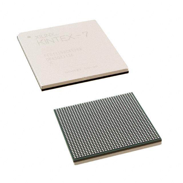
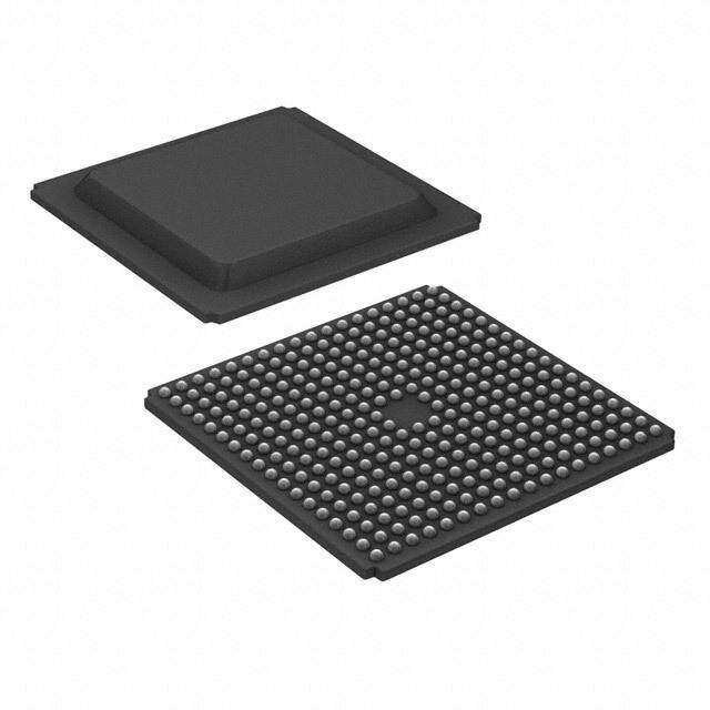
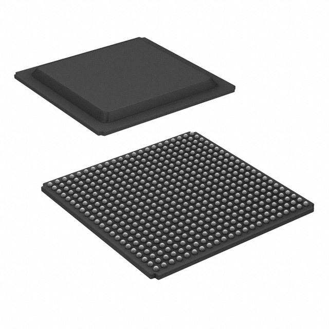
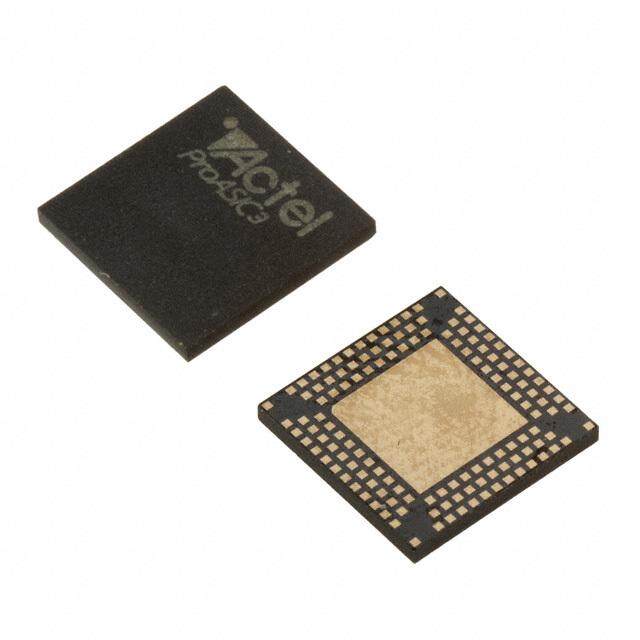
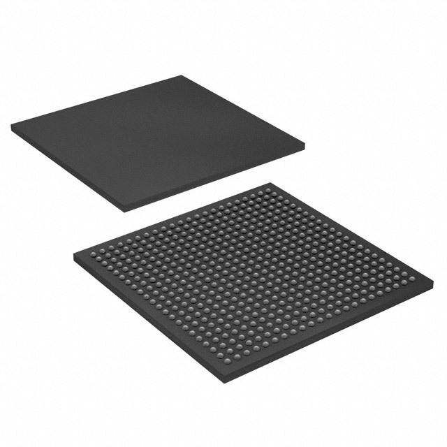
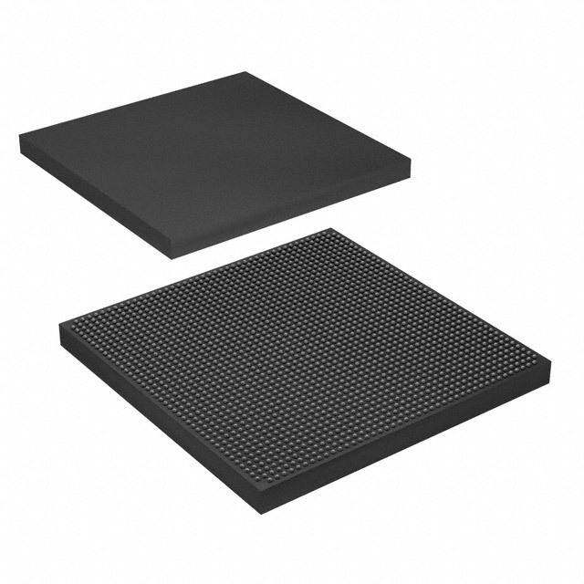
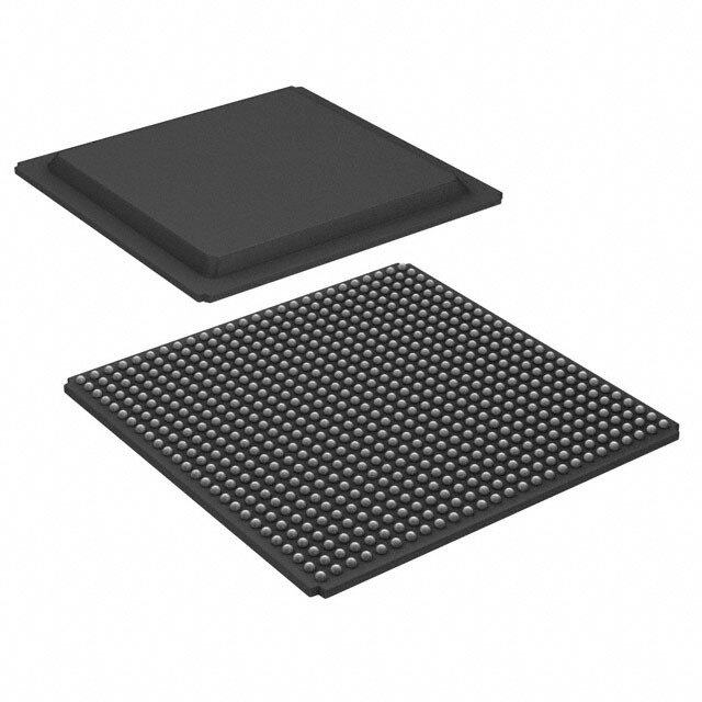
| 产品图片 |
|
| 产品型号 | EP2C20F256C7N |
| rohs | 无铅 / 符合限制有害物质指令(RoHS)规范要求 |
| 产品系列 | Cyclone® II |
| 产品培训模块 | http://www.digikey.cn/PTM/IndividualPTM.page?site=cn&lang=zhs&ptm=25450 |
| 供应商器件封装 | 256-FBGA(17x17) |
| 其它名称 | 544-1659 |
| 安装类型 | 表面贴装 |
| 封装/外壳 | 256-LBGA |
| 工作温度 | 0°C ~ 85°C |
| 总RAM位数 | 239616 |
| 栅极数 | - |
| 标准包装 | 90 |
| 电压-电源 | 1.15 V ~ 1.25 V |
| 逻辑元件/单元数 | 18752 |
| 配用 | /product-detail/zh/P0528/P0528-ND/1833602/product-detail/zh/DK-CYCII-2C20N/544-1736-ND/1207144 |




- 商务部:美国ITC正式对集成电路等产品启动337调查
- 曝三星4nm工艺存在良率问题 高通将骁龙8 Gen1或转产台积电
- 太阳诱电将投资9.5亿元在常州建新厂生产MLCC 预计2023年完工
- 英特尔发布欧洲新工厂建设计划 深化IDM 2.0 战略
- 台积电先进制程称霸业界 有大客户加持明年业绩稳了
- 达到5530亿美元!SIA预计今年全球半导体销售额将创下新高
- 英特尔拟将自动驾驶子公司Mobileye上市 估值或超500亿美元
- 三星加码芯片和SET,合并消费电子和移动部门,撤换高东真等 CEO
- 三星电子宣布重大人事变动 还合并消费电子和移动部门
- 海关总署:前11个月进口集成电路产品价值2.52万亿元 增长14.8%



PDF Datasheet 数据手册内容提取
1. Introduction CII51001-3.2 Introduction Following the immensely successful first-generation Cyclone® device family, Altera® CycloneII FPGAs extend the low-cost FPGA density range to 68,416 logic elements (LEs) and provide up to 622 usable I/O pins and up to 1.1 Mbits of embedded memory. Cyclone II FPGAs are manufactured on 300-mm wafers using TSMC's 90-nm low-k dielectric process to ensure rapid availability and low cost. By minimizing silicon area, Cyclone II devices can support complex digital systems on a single chip at a cost that rivals that of ASICs. Unlike other FPGA vendors who compromise power consumption and performance for low-cost, Altera’s latest generation of low-cost FPGAs—Cyclone II FPGAs, offer 60% higher performance and half the power consumption of competing 90-nm FPGAs. The low cost and optimized feature set of CycloneII FPGAs make them ideal solutions for a wide array of automotive, consumer, communications, video processing, test and measurement, and other end-market solutions. Reference designs, system diagrams, and IP, found at www.altera.com, are available to help you rapidly develop complete end-market solutions using CycloneII FPGAs. Low-Cost Embedded Processing Solutions Cyclone II devices support the Nios II embedded processor which allows you to implement custom-fit embedded processing solutions. Cyclone II devices can also expand the peripheral set, memory, I/O, or performance of embedded processors. Single or multiple Nios II embedded processors can be designed into a Cyclone II device to provide additional co-processing power or even replace existing embedded processors in your system. Using Cyclone II and Nios II together allow for low-cost, high-performance embedded processing solutions, which allow you to extend your product's life cycle and improve time to market over standard product solutions. Low-Cost DSP Solutions Use Cyclone II FPGAs alone or as DSP co-processors to improve price-to-performance ratios for digital signal processing (DSP) applications. You can implement high-performance yet low-cost DSP systems with the following Cyclone II features and design support: ■ Up to 150 18 × 18 multipliers ■ Up to 1.1 Mbit of on-chip embedded memory ■ High-speed interfaces to external memory Altera Corporation 1–1 February 2008
Features ■ DSP intellectual property (IP) cores ■ DSP Builder interface to The Mathworks Simulink and Matlab design environment ■ DSP Development Kit, Cyclone II Edition Cyclone II devices include a powerful FPGA feature set optimized for low-cost applications including a wide range of density, memory, embedded multiplier, and packaging options. Cyclone II devices support a wide range of common external memory interfaces and I/O protocols required in low-cost applications. Parameterizable IP cores from Altera and partners make using Cyclone II interfaces and protocols fast and easy. Features The Cyclone II device family offers the following features: ■ High-density architecture with 4,608 to 68,416 LEs ● M4K embedded memory blocks ● Up to 1.1 Mbits of RAM available without reducing available logic ● 4,096 memory bits per block (4,608 bits per block including 512 parity bits) ● Variable port configurations of ×1, ×2, ×4, ×8, ×9, ×16, ×18, ×32, and ×36 ● True dual-port (one read and one write, two reads, or two writes) operation for ×1, ×2, ×4, ×8, ×9, ×16, and ×18 modes ● Byte enables for data input masking during writes ● Up to 260-MHz operation ■ Embedded multipliers ● Up to 150 18- × 18-bit multipliers are each configurable as two independent 9- × 9-bit multipliers with up to 250-MHz performance ● Optional input and output registers ■ Advanced I/O support ● High-speed differential I/O standard support, including LVDS, RSDS, mini-LVDS, LVPECL, differential HSTL, and differential SSTL ● Single-ended I/O standard support, including 2.5-V and 1.8-V, SSTL class I and II, 1.8-V and 1.5-V HSTL class I and II, 3.3-V PCI and PCI-X 1.0, 3.3-, 2.5-, 1.8-, and 1.5-V LVCMOS, and 3.3-, 2.5-, and 1.8-V LVTTL ● Peripheral Component Interconnect Special Interest Group (PCI SIG) PCI Local Bus Specification, Revision 3.0 compliance for 3.3-V operation at 33 or 66 MHz for 32- or 64-bit interfaces ● PCI Express with an external TI PHY and an Altera PCI Express ×1 Megacore® function 1–2 Altera Corporation Cyclone II Device Handbook, Volume 1 February 2008
Introduction ● 133-MHz PCI-X 1.0 specification compatibility ● High-speed external memory support, including DDR, DDR2, and SDR SDRAM, and QDRII SRAM supported by drop in Altera IP MegaCore functions for ease of use ● Three dedicated registers per I/O element (IOE): one input register, one output register, and one output-enable register ● Programmable bus-hold feature ● Programmable output drive strength feature ● Programmable delays from the pin to the IOE or logic array ● I/O bank grouping for unique VCCIO and/or VREF bank settings ● MultiVolt™ I/O standard support for 1.5-, 1.8-, 2.5-, and 3.3-interfaces ● Hot-socketing operation support ● Tri-state with weak pull-up on I/O pins before and during configuration ● Programmable open-drain outputs ● Series on-chip termination support ■ Flexible clock management circuitry ● Hierarchical clock network for up to 402.5-MHz performance ● Up to four PLLs per device provide clock multiplication and division, phase shifting, programmable duty cycle, and external clock outputs, allowing system-level clock management and skew control ● Up to 16 global clock lines in the global clock network that drive throughout the entire device ■ Device configuration ● Fast serial configuration allows configuration times less than 100 ms ● Decompression feature allows for smaller programming file storage and faster configuration times ● Supports multiple configuration modes: active serial, passive serial, and JTAG-based configuration ● Supports configuration through low-cost serial configuration devices ● Device configuration supports multiple voltages (either 3.3, 2.5, or 1.8 V) ■ Intellectual property ● Altera megafunction and Altera MegaCore function support, and Altera Megafunctions Partners Program (AMPPSM) megafunction support, for a wide range of embedded processors, on-chip and off-chip interfaces, peripheral functions, DSP functions, and communications functions and Altera Corporation 1–3 February 2008 Cyclone II Device Handbook, Volume 1
Features protocols. Visit the Altera IPMegaStore at www.altera.com to download IP MegaCore functions. ● Nios II Embedded Processor support The Cyclone II family offers devices with the Fast-On feature, which offers a faster power-on-reset (POR) time. Devices that support the Fast-On feature are designated with an “A” in the device ordering code. For example, EP2C5A, EP2C8A, EP2C15A, and EP2C20A. The EP2C5A is only available in the automotive speed grade. The EP2C8A and EP2C20A are only available in the industrial speed grade. The EP2C15A is only available with the Fast-On feature and is available in both commercial and industrial grades. The Cyclone II “A” devices are identical in feature set and functionality to the non-A devices except for support of the faster POR time. f Cyclone II A devices are offered in automotive speed grade. For more information, refer to the Cyclone II section in the Automotive-Grade Device Handbook. f For more information on POR time specifications for CycloneII A and non-A devices, refer to the Hot Socketing & Power-On Reset chapter in the CycloneII Device Handbook. Table1–1 lists the CycloneII device family features. Table1–2 lists the CycloneII device package offerings and maximum user I/O pins. Table1–1.CycloneII FPGA Family Features (Part 1 of2) Feature EP2C5 (2) EP2C8 (2) EP2C15 (1) EP2C20 (2) EP2C35 EP2C50 EP2C70 LEs 4,608 8,256 14,448 18,752 33,216 50,528 68,416 M4K RAM blocks (4 26 36 52 52 105 129 250 Kbits plus 512parity bits Total RAM bits 119,808 165,888 239,616 239,616 483,840 594,432 1,152,00 0 Embedded 13 18 26 26 35 86 150 multipliers (3) PLLs 2 2 4 4 4 4 4 1–4 Altera Corporation Cyclone II Device Handbook, Volume 1 February 2008
Introduction Table1–1.CycloneII FPGA Family Features (Part 2 of2) Feature EP2C5 (2) EP2C8 (2) EP2C15 (1) EP2C20 (2) EP2C35 EP2C50 EP2C70 Maximum user 158 182 315 315 475 450 622 I/Opins Notes to Table1–1: (1) The EP2C15A is only available with the Fast On feature, which offers a faster POR time. This device is available in both commercial and industrial grade. (2) The EP2C5, EP2C8, and EP2C20 optionally support the Fast On feature, which is designated with an “A” in the device ordering code. The EP2C5A is only available in the automotive speed grade. The EP2C8A and EP2C20A devices are only available in industrial grade. (3) This is the total number of 18 × 18 multipliers. For the total number of 9 × 9 multipliers per device, multiply the total number of 18 × 18 multipliers by 2. Altera Corporation 1–5 February 2008 Cyclone II Device Handbook, Volume 1
Features Table1–2.CycloneII Package Options & Maximum User I/O Pins Notes(1) (2) 484-Pin 256-Pin 484-Pin 672-Pin 896-Pin 144-Pin 208-Pin 240-Pin Ultra Device FineLine FineLine FineLine FineLine TQFP (3) PQFP (4) PQFP FineLine BGA BGA BGA BGA BGA EP2C5 (6) (8) 89 142 — 158 (5) — — — — EP2C8 (6) 85 138 — 182 — — — — EP2C8A (6), (7) — — — 182 — — — — EP2C15A (6), (7) — — — 152 315 — — — EP2C20 (6) — — 142 152 315 — — — EP2C20A (6), (7) — — — 152 315 — — — EP2C35 (6) — — — — 322 322 475 — EP2C50 (6) — — — — 294 294 450 — EP2C70 (6) — — — — — — 422 622 Notes to Table1–2: (1) CycloneII devices support vertical migration within the same package (for example, you can migrate between the EP2C20 device in the 484-pin FineLine BGA package and the EP2C35 and EP2C50 devices in the same package). (2) The Quartus® II software I/O pin counts include four additional pins, TDI, TDO, TMS, and TCK, which are not available as general purpose I/O pins. (3) TQFP: thin quad flat pack. (4) PQFP: plastic quad flat pack. (5) Vertical migration is supported between the EP2C5F256 and the EP2C8F256 devices. However, not all of the DQ and DQS groups are supported. Vertical migration between the EP2C5 and the EP2C15 in the F256 package is not supported. (6) The I/O pin counts for the EP2C5, EP2C8, and EP2C15A devices include 8 dedicated clock pins that can be used for data inputs. The I/O counts for the EP2C20, EP2C35, EP2C50, and EP2C70 devices include 16 dedicated clock pins that can be used for data inputs. (7) EP2C8A, EP2C15A, and EP2C20A have a Fast On feature that has a faster POR time. The EP2C15A is only available with the Fast On option. (8) The EP2C5 optionally support the Fast On feature, which is designated with an “A” in the device ordering code. The EP2C5A is only available in the automotive speed grade. Refer to the Cyclone II section in the Automotive-Grade Device Handbook. CycloneII devices support vertical migration within the same package (for example, you can migrate between the EP2C35, EPC50, and EP2C70 devices in the 672-pin FineLine BGA package). The exception to vertical migration support within the CycloneII family is noted in Table1–3. 1–6 Altera Corporation Cyclone II Device Handbook, Volume 1 February 2008
Introduction Vertical migration means that you can migrate to devices whose dedicated pins, configuration pins, and power pins are the same for a given package across device densities. Table1–3.Total Number of Non-Migratable I/O Pins for CycloneII Vertical Migration Paths 256-Pin 484-Pin 672-Pin Vertical 208-Pin 484-Pin Ultra 144-Pin TQFP FineLine BGA FineLine BGA FineLine BGA Migration Path PQFP FineLine BGA (1) (2) (3) EP2C5 to 4 4 1 (4) — — — EP2C8 EP2C8 to — — 30 — — — EP2C15 EP2C15 to — — 0 0 — — EP2C20 EP2C20 to — — 16 — — EP2C35 EP2C35 to — — — 28 28 (5) 28 EP2C50 EP2C50 to — — — — 28 28 EP2C70 Notes to Table1–3: (1) Vertical migration between the EP2C5F256 to the EP2C15AF256 and the EP2C5F256 to the EP2C20F256 devices is not supported. (2) When migrating from the EP2C20F484 device to the EP2C50F484 device, a total of 39 I/O pins are non-migratable. (3) When migrating from the EP2C35F672 device to the EP2C70F672 device, a total of 56 I/O pins are non-migratable. (4) In addition to the one non-migratable I/O pin, there are 34 DQ pins that are non-migratable. (5) The pinouts of 484 FBGA and 484 UBGA are the same. 1 When moving from one density to a larger density, I/O pins are often lost because of the greater number of power and ground pins required to support the additional logic within the larger device. For I/O pin migration across densities, you must cross reference the available I/O pins using the device pin-outs for all planned densities of a given package type to identify which I/O pins are migratable. To ensure that your board layout supports migratable densities within one package offering, enable the applicable vertical migration path within the QuartusII software (go to Assignments menu, then Device, then click the Migration Devices button). After compilation, check the information messages for a full list of I/O, DQ, LVDS, and other pins that are not available because of the selected migration path. Table1–3 lists the CycloneII device package offerings and shows the total number of non-migratable I/O pins when migrating from one density device to a larger density device. Altera Corporation 1–7 February 2008 Cyclone II Device Handbook, Volume 1
Features CycloneII devices are available in up to three speed grades: –6, –7, and –8, with –6 being the fastest. Table1–4 shows the CycloneII device speed-grade offerings. Table1–4.CycloneII Device Speed Grades 484-Pin 256-Pin 484-Pin 672-Pin 896-Pin 144-Pin 208-Pin 240-Pin Ultra Device FineLine FineLine FineLine FineLine TQFP PQFP PQFP FineLine BGA BGA BGA BGA BGA EP2C5 (1) –6, –7, –8 –7, –8 — –6, –7, –8 — — — — EP2C8 –6, –7, –8 –7, –8 — –6, –7, –8 — — — — EP2C8A (2) — — — –8 — — — — EP2C15A — — — –6, –7, –8 –6, –7, –8 — — — EP2C20 — — –8 –6, –7, –8 –6, –7, –8 — — — EP2C20A (2) — — — –8 –8 — — — EP2C35 — — — — –6, –7, –8 –6, –7, –8 –6, –7, –8 — EP2C50 — — — — –6, –7, –8 –6, –7, –8 –6, –7, –8 — EP2C70 — — — — — — –6, –7, –8 –6, –7, –8 Notes to Table1–4: (1) The EP2C5 optionally support the Fast On feature, which is designated with an “A” in the device ordering code. The EP2C5A is only available in the automotive speed grade. Refer to the Cyclone II section in the Automotive-Grade Device Handbook for detailed information. (2) EP2C8A and EP2C20A are only available in industrial grade. 1–8 Altera Corporation Cyclone II Device Handbook, Volume 1 February 2008
Introduction Referenced This chapter references the following documents: Documents ■ Hot Socketing & Power-On Reset chapter in Cyclone II Device Handbook ■ Automotive-Grade Device Handbook Document Table1–5 shows the revision history for this document. Revision History Table1–5.Document Revision History Date & Document Changes Made Summary of Changes Version February 2008 ● Added “Referenced Documents”. — v3.2 ● Updated “Features” section and Table1–1, Table1–2, and Table1–4 with information about EP2C5A. February 2007 ● Added document revision history. Note to explain difference v3.1 ● Added new Note(2) to Table1–2. between I/O pin count information provided in Table1–2 and in the Quartus II software documentation. November 2005 ● Updated Introduction and Features. — v2.1 ● Updated Table1–3. July 2005 v2.0 ● Updated technical content throughout. — ● Updated Table1–2. ● Added Tables1–3 and 1–4. November 2004 ● Updated Table1–2. — v1.1 ● Updated bullet list in the “Features” section. June 2004 v1.0 Added document to the CycloneII Device Handbook. — Altera Corporation 1–9 February 2008 Cyclone II Device Handbook, Volume 1
Document Revision History 1–10 Altera Corporation Cyclone II Device Handbook, Volume 1 February 2008
Mouser Electronics Authorized Distributor Click to View Pricing, Inventory, Delivery & Lifecycle Information: I ntel: EP2C15AF484C8N EP2C20F256C7 EP2C20F484C7N EP2C20F484C8N EP2C20Q240C8 EP2C35F484C6N EP2C35F484C7N EP2C35F484C8 EP2C35F484I8 EP2C35F484I8N EP2C35F672C6N EP2C35F672C8 EP2C35F672I8N EP2C35U484C7N EP2C50F484I8 EP2C50F672C6N EP2C50F672C7N EP2C50F672C8 EP2C50F672C8N EP2C50F672I8N EP2C50U484C6N EP2C50U484I8N EP2C5AT144A7N EP2C5F256C6N EP2C5F256C8N EP2C5F256I8 EP2C5Q208I8N EP2C5T144C6N EP2C5T144C7N EP2C5T144C8 EP2C5T144C8N EP2C70F672C7 EP2C70F672C7N EP2C70F672C8 EP2C70F672I8 EP2C70F896C6N EP2C70F896C7 EP2C70F896C8N EP2C70F896I8 EP2C70F896I8N EP2C8F256C6 EP2C8Q208C7 EP2C8Q208C7N EP2C8Q208C8 EP2C8Q208I8 EP2C8Q208I8N EP2C8T144C6N EP2C8T144C8N EP2C15AF256A7N EP2C15AF256C6N EP2C15AF256C7N EP2C15AF256C8N EP2C15AF256I8N EP2C15AF484A7N EP2C15AF484C6N EP2C15AF484C7N EP2C15AF484I8N EP2C20AF256A7N EP2C20AF256I8N EP2C20AF484A7N EP2C20AF484I8N EP2C20F256C6 EP2C20F256C6N EP2C20F256C7N EP2C20F256C8 EP2C20F256C8N EP2C20F256I8 EP2C20F256I8N EP2C20F484C6 EP2C20F484C6N EP2C20F484C7 EP2C20F484C8 EP2C20F484I8 EP2C20F484I8N EP2C20Q240C8N EP2C35F484C6 EP2C35F484C7 EP2C35F484C8N EP2C35F672C6 EP2C35F672C7 EP2C35F672C7N EP2C35F672C8N EP2C35F672I8 EP2C35U484C6 EP2C35U484C6N EP2C35U484C7 EP2C35U484C8 EP2C35U484C8N EP2C35U484I8 EP2C35U484I8N EP2C50F484C6 EP2C50F484C6N EP2C50F484C7 EP2C50F484C7N EP2C50F484C8 EP2C50F484C8N EP2C50F484I8N EP2C50F672C6 EP2C50F672C7 EP2C50F672I8
 Datasheet下载
