ICGOO在线商城 > EMIF06-1005M12
 Datasheet下载
- 型号: EMIF06-1005M12
- 制造商: STMicroelectronics
- 库位|库存: xxxx|xxxx
- 要求:
| 数量阶梯 | 香港交货 | 国内含税 |
| +xxxx | $xxxx | ¥xxxx |
查看当月历史价格
查看今年历史价格
EMIF06-1005M12产品简介:
ICGOO电子元器件商城为您提供EMIF06-1005M12由STMicroelectronics设计生产,在icgoo商城现货销售,并且可以通过原厂、代理商等渠道进行代购。 提供EMIF06-1005M12价格参考¥3.67-¥5.55以及STMicroelectronicsEMIF06-1005M12封装/规格参数等产品信息。 你可以下载EMIF06-1005M12参考资料、Datasheet数据手册功能说明书, 资料中有EMIF06-1005M12详细功能的应用电路图电压和使用方法及教程。
| 参数 | 数值 |
| 产品目录 | |
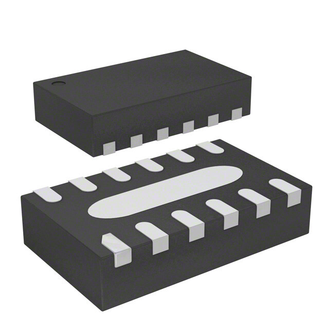
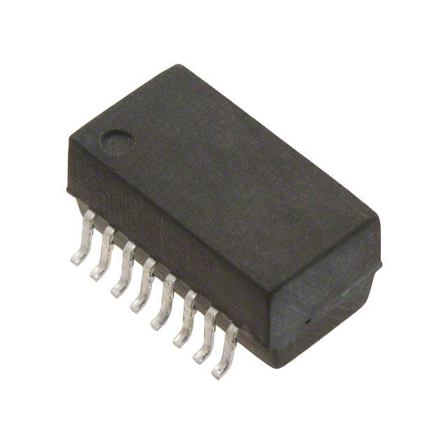
| 描述 | IC EMI FILTER 6LINE 12-MICRO QFNESD 抑制器 6lin lw cpcitnc EMI 45pF -35db @ 900MHz |
| ESD保护 | 是 |
| 产品分类 | EMI/RFI 滤波器(LC、RC 网络)ESD 抑制器 |
| 品牌 | STMicroelectronics |
| 产品手册 | |
| 产品图片 |
|
| rohs | 符合RoHS无铅 / 符合限制有害物质指令(RoHS)规范要求 |
| 产品系列 | STMicroelectronics EMIF06-1005M12EMIF |
| 数据手册 | |
| 产品型号 | EMIF06-1005M12 |
| 中心/截止频率 | - |
| 产品目录页面 | |
| 产品种类 | ESD 抑制器 |
| 其它名称 | 497-7740-2 |
| 其它有关文件 | http://www.st.com/web/catalog/sense_power/FM139/CL1432/SC1433/PF144567?referrer=70071840http://www.st.com/web/catalog/sense_power/FM139/CL1432/SC1437/PF144567?referrer=70071840 |
| 包装 | 带卷 (TR) |
| 商标 | STMicroelectronics |
| 大小/尺寸 | 0.098" 长x 0.059" 宽(2.50mm x 1.50mm) |
| 封装 | Reel |
| 封装/外壳 | 12-UFDFN 裸露焊盘 |
| 工作温度 | -40°C ~ 85°C |
| 工厂包装数量 | 3000 |
| 应用 | 移动设备的数据线路 |
| 技术 | RC(Pi) |
| 数值 | R = 100 欧姆,C = 45pF(总计) |
| 标准包装 | 3,000 |
| 滤波器阶数 | 2nd |
| 电流 | 10mA |
| 电阻-通道(Ω) | 100 |
| 类型 | 低通 |
| 系列 | EMIF06-1005M12 |
| 衰减值 | 34dB @ 900MHz ~ 1.8GHz |
| 通道数 | 6 |
| 高度 | 0.024"(0.60mm) |


- 商务部:美国ITC正式对集成电路等产品启动337调查
- 曝三星4nm工艺存在良率问题 高通将骁龙8 Gen1或转产台积电
- 太阳诱电将投资9.5亿元在常州建新厂生产MLCC 预计2023年完工
- 英特尔发布欧洲新工厂建设计划 深化IDM 2.0 战略
- 台积电先进制程称霸业界 有大客户加持明年业绩稳了
- 达到5530亿美元!SIA预计今年全球半导体销售额将创下新高
- 英特尔拟将自动驾驶子公司Mobileye上市 估值或超500亿美元
- 三星加码芯片和SET,合并消费电子和移动部门,撤换高东真等 CEO
- 三星电子宣布重大人事变动 还合并消费电子和移动部门
- 海关总署:前11个月进口集成电路产品价值2.52万亿元 增长14.8%


PDF Datasheet 数据手册内容提取
EMIF06-1005M12 6-line IPAD™ low capacitance EMI filter and ESD protection in micro QFN package Features 12 1 ■ EMI symmetrical (I/O) low-pass filter 11 2 ■ High efficiency in EMI filtering: -34 dB at 10 3 frequencies from 900 MHz to 1.8 GHz GND 9 4 ■ Very low PCB space consumption: 8 5 2.5 mm x 1.5 mm 7 6 ■ Very thin package: 0.6 mm max Micro QFN 2.5 mm x 1.5 mm ■ High efficiency in ESD suppression on inputs (bottom view) pins (IEC 61000-4-2 level 4) ■ High reliability offered by monolithic integration Figure 1. Pin configuration (top view) ■ High reduction of parasitic elements through integration and wafer level packaging 1 Input Output 12 ■ Lead-free package 2 Input Output 11 Complies with following standards: ■ IEC 61000-4-2 level 4 input and output pins 3 Input Output 10 – 15 kV (air discharge) – 8 kV (contact discharge) 4 Input Output 9 ■ MIL STD 883G - Method 3015-7 Class 3B (all pins) 5 Input Output 8 Applications 6 Input Output 7 Where EMI filtering in ESD sensitive equipment is required: Figure 2. Basic cell configuration ■ LCD and camera for mobile phones ■ Computers and printers 100Ω Input Output ■ Communication systems ■ MCU boards Description Typical line capacitance = 45 pF @ 0V EMIF06-1005M12 is a 6-line, highly integrated device designed to suppress EMI/RFI noise in all systems exposed to electromagnetic interference. This filter includes ESD protection circuitry, which prevents damage to the application when subjected to ESD surges up to 15 kV on the input pins. TM: IPAD is a trademark of STMicroelectronics February 2008 Rev 3 1/10 www.st.com
Characteristics EMIF06-1005M12 1 Characteristics Table 1. A bsolute ratings (limiting values at T = 25 °C unless otherwise specified) amb Symbol Parameter Value Unit ESD IEC 61000-4-2, air discharge 15 V kV PP ESD IEC 61000-4-2, contact discharge 15 T Junction temperature 125 °C j T Operating temperature range -40 to + 85 °C op T Storage temperature range -55 to +150 °C stg Table 2. E lectrical characteristics (T = 25 °C) amb Symbol Parameter I V Breakdown voltage BR IF I Leakage current @ V RM RM V Stand-off voltage RM VCL Clamping voltage VCVLBR VRM VF V IRM Rd Dynamic resistance IR I Peak pulse current PP R Series resistance between Input & Output I/O IPP C Input capacitance per line line Symbol Test conditions Min. Typ. Max. Unit V I = 1 mA 6 8 10 V BR R V I = 10 mA 0.5 1.0 1.5 F F I V = 3 V per line 200 nA RM RM R Tolerance ± 10% 90 100 110 Ω I/O C V = 0 V dc, V = 30 mV, F = 1 MHz 38 45 52 pF line LINE OSC Figure 3. S 21 attenuation measurement Figure 4. Analog cross talk measurements dB dB 0.00 0.00 -10.00 -20.00 -10.00 -30.00 -40.00 -20.00 -50.00 -60.00 -70.00 -30.00 -80.00 F (Hz) -90.00 F (Hz) -40.00 -100.00 100.0k 1.0M 10.0M 100.0M 1.0G 1.0M 3.0M 10.0M 30.0M 100.0M300.0M 1.0G 3.0G 2/10
EMIF06-1005M12 Ordering information scheme Figure 5. E SD response to IEC 61000-4-2 Figure 6. ESD response to IEC 61000-4-2 (+15 kV air discharge) on one input (-15 kV air discharge) on one input (V ) and on one output (V ) (V ) and on one output (V ) in out in out Figure 7. Line capacitance versus reverse voltage applied (typical value) C (pF) 50.00 LINE 45.00 40.00 35.00 30.00 25.00 20.00 15.00 10.00 5.00 V (V) LINE 0.00 0 1 2 3 4 5 2 Ordering information scheme Figure 8. Ordering information scheme EMIF yy - xxx z Mx EMI Filter Number of lines Information x = resistance value (Ohms) z = capacitance value / 10(pF) Package Mx = Micro QFN x leads 3/10
Package information EMIF06-1005M12 3 Package information ● Epoxy meets UL94, V0 In order to meet environmental requirements, ST offers these devices in ECOPACK® packages. These packages have a lead-free second level interconnect. The category of second level interconnect is marked on the inner box label, in compliance with JEDEC Standard JESD97. The maximum ratings related to soldering conditions are also marked on the inner box label. ECOPACK is an ST trademark. ECOPACK specifications are available at www.st.com. T able 3. QFN 2.5 x 1.5 package dimensions Dimensions D N Ref Millimeters inches E MIN TYP MAX MIN TYP MAX A 0.50 0.55 0.60 0.20 0.22 0.24 1 2 A1 0.00 0.02 0.05 0.00 0.01 0.02 A b 0.15 0.18 0.25 0.06 0.07 0.10 A1 D 2.50 0.98 D2 D2 1.70 1.80 1.90 0.67 0.71 0.75 1 2 E 1.50 0.59 L E2 0.30 0.40 0.50 0.12 0.16 0.24 E2 k e 0.40 0.16 N b k 0.20 0.08 e L 0.25 0.30 0.35 0.10 0.12 0.14 F igure 9. Footprint Figure 10. Marking 0.40 0.20 Dot:Pin 1 Identification X=Marking 0.60 YWW=Data code 0.25 (Y=year XXYY 0.40 2.10 WW= week wwww 1.80 4/10
EMIF06-1005M12 Package information Figure 11. Tape and reel specification 22..00++//--00..0055 44..0000++//--00..11 ff11..55 ++//--00..11 11 .7.7 55 ++ /-/- 00 .1.1 33 .5.5 ++ /-/- 8.18.1 0.050.05 +/-+/- 22 XXXYYY XXXYYY XXXYYY 0.10.1 .70.70 wwwwww wwwwww wwwwww 00..7755 11..7700 44..0000 UUsseerr ddiirreeccttiioonn ooff uunnrreeeelliinngg Note: Product marking may be rotated by 90° for assembly plant differentiation. In no case should this product marking be used to orient the component for its placement on a PCB. Only pin1 mark is to be used for this purpose. 5/10
Recommendation on PCB assembly EMIF06-1005M12 4 Recommendation on PCB assembly 4.1 Stencil opening design 1. General recommendation on stencil opening design a) Stencil opening dimensions: L (Length), W (Width), T (Thickness). Figure 12. Stencil opening dimensions L T W b) General design rule Stencil thickness (T) = 75 ~ 125 µm W Aspect Ratio = -----≥1.5 T L×W Aspect Area = ----------------------------≥0.66 2T(L+W) 2. Reference design a) Stencil opening thickness: 100 µm b) Stencil opening for central exposed pad: Opening to footprint ratio is 50%. c) Stencil opening for leads: Opening to footprint ratio is 90%. Figure 13. Recommended stencil window position 5µm 5µm 15µm 600µm 570µm 0.40 0.20 0.60 190µm 0.25 15µm 0.40 2.10 200µm 1800µm 50µm 1.80 m µ 400µm 0 0 3 1224µm Footprint 50µm Stencilwindow 288µm 288µm Footprint 6/10
EMIF06-1005M12 Recommendation on PCB assembly 4.2 Solder paste 1. Halide-free flux qualification ROL0 according to ANSI/J-STD-004. 2. “No clean” solder paste is recommended. 3. Offers a high tack force to resist component movement during high speed 4. Solder paste with fine particles: powder particle size is 20-45 µm. 4.3 Placement 1. Manual positioning is not recommended. 2. It is recommended to use the lead recognition capabilities of the placement system, not the outline centering 3. Standard tolerance of ± 0.05 mm is recommended. 4. 3.5 N placement force is recommended. Too much placement force can lead to squeezed out solder paste and cause solder joints to short. Too low placement force can lead to insufficient contact between package and solder paste that could cause open solder joints or badly centered packages. 5. To improve the package placement accuracy, a bottom side optical control should be performed with a high resolution tool. 6. For assembly, a perfect supporting of the PCB (all the more on flexible PCB) is recommended during solder paste printing, pick and place and reflow soldering by using optimized tools. 4.4 PCB design preference 1. To control the solder paste amount, the closed via is recommended instead of open vias. 2. The position of tracks and open vias in the solder area should be well balanced. The symmetrical layout is recommended, in case any tilt phenomena caused by asymmetrical solder paste amount due to the solder flow away. 7/10
Recommendation on PCB assembly EMIF06-1005M12 4.5 Reflow profile Figure 14. ST ECOPACK® recommended soldering reflow profile for PCB mounting TTeemmppeerraattuurree ((°°CC)) 226600°°CC mmaaxx 225555°°CC 222200°°CC 118800°°CC 112255 °°CC 2°C/s 2r°eCc/osm remceonmdmedended 3°C/s max 6°C/s max 6°C/s max 3°C/s max 00 00 11 22 33 44 55 66 77 1100--3300 sseecc TTiimmee ((mmiinn)) 9900 ttoo 115500 sseecc 9900 sseecc mmaaxx Note: Minimize air convection currents in the reflow oven to avoid component movement. 8/10
EMIF06-1005M12 Ordering information 5 Ordering information T able 4. Ordering information Order code Marking Package Weight Base qty Delivery mode EMIF06-1005M12 F(1) Micro QFN 6 mg 3000 Tape and reel (7”) 1. The marking can be rotated by 90° to differentiate assembly location 6 Revision history T able 5. Document revision history Date Revision Changes 3-Jul-2006 1 Initial release. 1-Feb-2007 2 Added note on marking rotation in section 3. Package information. Reformatted to current standards. Updated ECOPACK statement. 04-Feb-2008 3 Updated Section4: Recommendation on PCB assembly. 9/10
EMIF06-1005M12 Please Read Carefully: Information in this document is provided solely in connection with ST products. STMicroelectronics NV and its subsidiaries (“ST”) reserve the right to make changes, corrections, modifications or improvements, to this document, and the products and services described herein at any time, without notice. All ST products are sold pursuant to ST’s terms and conditions of sale. Purchasers are solely responsible for the choice, selection and use of the ST products and services described herein, and ST assumes no liability whatsoever relating to the choice, selection or use of the ST products and services described herein. No license, express or implied, by estoppel or otherwise, to any intellectual property rights is granted under this document. If any part of this document refers to any third party products or services it shall not be deemed a license grant by ST for the use of such third party products or services, or any intellectual property contained therein or considered as a warranty covering the use in any manner whatsoever of such third party products or services or any intellectual property contained therein. UNLESS OTHERWISE SET FORTH IN ST’S TERMS AND CONDITIONS OF SALE ST DISCLAIMS ANY EXPRESS OR IMPLIED WARRANTY WITH RESPECT TO THE USE AND/OR SALE OF ST PRODUCTS INCLUDING WITHOUT LIMITATION IMPLIED WARRANTIES OF MERCHANTABILITY, FITNESS FOR A PARTICULAR PURPOSE (AND THEIR EQUIVALENTS UNDER THE LAWS OF ANY JURISDICTION), OR INFRINGEMENT OF ANY PATENT, COPYRIGHT OR OTHER INTELLECTUAL PROPERTY RIGHT. UNLESS EXPRESSLY APPROVED IN WRITING BY AN AUTHORIZED ST REPRESENTATIVE, ST PRODUCTS ARE NOT RECOMMENDED, AUTHORIZED OR WARRANTED FOR USE IN MILITARY, AIR CRAFT, SPACE, LIFE SAVING, OR LIFE SUSTAINING APPLICATIONS, NOR IN PRODUCTS OR SYSTEMS WHERE FAILURE OR MALFUNCTION MAY RESULT IN PERSONAL INJURY, DEATH, OR SEVERE PROPERTY OR ENVIRONMENTAL DAMAGE. ST PRODUCTS WHICH ARE NOT SPECIFIED AS "AUTOMOTIVE GRADE" MAY ONLY BE USED IN AUTOMOTIVE APPLICATIONS AT USER’S OWN RISK. Resale of ST products with provisions different from the statements and/or technical features set forth in this document shall immediately void any warranty granted by ST for the ST product or service described herein and shall not create or extend in any manner whatsoever, any liability of ST. ST and the ST logo are trademarks or registered trademarks of ST in various countries. Information in this document supersedes and replaces all information previously supplied. The ST logo is a registered trademark of STMicroelectronics. All other names are the property of their respective owners. © 2008 STMicroelectronics - All rights reserved STMicroelectronics group of companies Australia - Belgium - Brazil - Canada - China - Czech Republic - Finland - France - Germany - Hong Kong - India - Israel - Italy - Japan - Malaysia - Malta - Morocco - Singapore - Spain - Sweden - Switzerland - United Kingdom - United States of America www.st.com 10/10
Mouser Electronics Authorized Distributor Click to View Pricing, Inventory, Delivery & Lifecycle Information: S TMicroelectronics: EMIF06-1005M12