ICGOO在线商城 > EMIF03-SIM05F3
 Datasheet下载
- 型号: EMIF03-SIM05F3
- 制造商: STMicroelectronics
- 库位|库存: xxxx|xxxx
- 要求:
| 数量阶梯 | 香港交货 | 国内含税 |
| +xxxx | $xxxx | ¥xxxx |
查看当月历史价格
查看今年历史价格
EMIF03-SIM05F3产品简介:
ICGOO电子元器件商城为您提供EMIF03-SIM05F3由STMicroelectronics设计生产,在icgoo商城现货销售,并且可以通过原厂、代理商等渠道进行代购。 提供EMIF03-SIM05F3价格参考以及STMicroelectronicsEMIF03-SIM05F3封装/规格参数等产品信息。 你可以下载EMIF03-SIM05F3参考资料、Datasheet数据手册功能说明书, 资料中有EMIF03-SIM05F3详细功能的应用电路图电压和使用方法及教程。
| 参数 | 数值 |
| 产品目录 | |
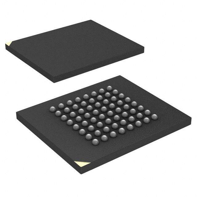
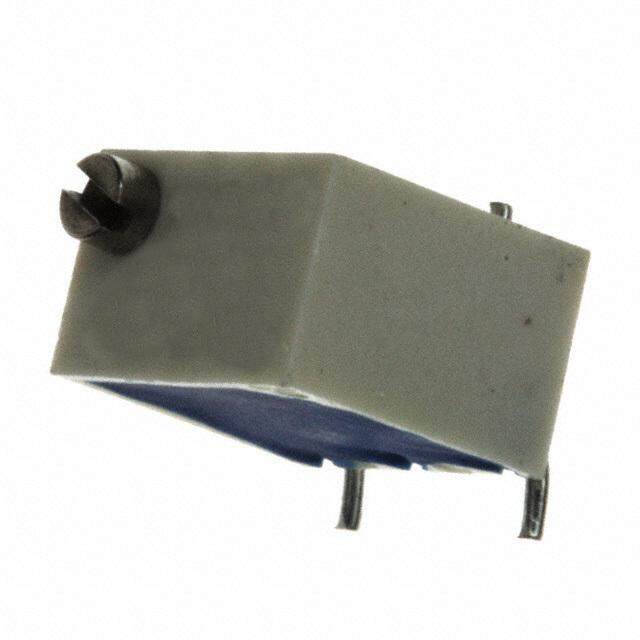
| 描述 | IC EMI FILTER ESD PROT 9FLIPCHIPEMI滤波珠子、芯片与阵列 EMI filter SWP 100nA 6V 12pF |
| ESD保护 | 是 |
| 产品分类 | EMI/RFI 滤波器(LC、RC 网络)EMI/RFI 器件 |
| 品牌 | STMicroelectronics |
| 产品手册 | |
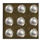
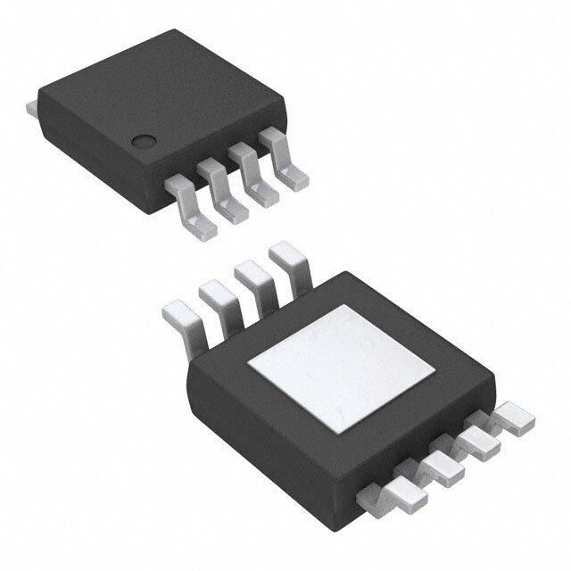
| 产品图片 |
|
| rohs | 符合RoHS无铅 / 符合限制有害物质指令(RoHS)规范要求 |
| 产品系列 | EMI滤波珠子、芯片与阵列,STMicroelectronics EMIF03-SIM05F3EMIF |
| mouser_ship_limit | 该产品可能需要其他文件才能进口到中国。 |
| 数据手册 | |
| 产品型号 | EMIF03-SIM05F3 |
| 中心/截止频率 | - |
| 产品 | EMI Filter Arrays |
| 产品种类 | EMI滤波珠子、芯片与阵列 |
| 其它名称 | 497-13475-6 |
| 其它有关文件 | http://www.st.com/web/catalog/sense_power/FM139/CL1432/SC1435/PF253956?referrer=70071840 |
| 包装 | Digi-Reel® |
| 商标 | STMicroelectronics |
| 外壳宽度 | 1.22 mm |
| 外壳长度 | 1.22 mm |
| 大小/尺寸 | 0.048" 长x 0.048" 宽 (1.22mm x 1.22mm) |
| 封装 | Reel |
| 封装/外壳 | 9-UFBGA,WLCSP |
| 封装/箱体 | WLCSP-9 |
| 尺寸 | 1.22 mm W x 1.22 mm L |
| 工作温度 | -30°C ~ 85°C |
| 工作温度范围 | - 30 C to + 85 C |
| 工厂包装数量 | 5000 |
| 应用 | SIM 卡 |
| 技术 | RC(Pi) |
| 数值 | R = 47,100 欧姆,C = 12pF |
| 标准包装 | 1 |
| 滤波器阶数 | 2nd |
| 电压额定值 | 6 V |
| 电容 | 12 pF |
| 电流 | - |
| 电阻-通道(Ω) | 47,100 |
| 端接类型 | SMD/SMT |
| 类型 | 低通 |
| 系列 | EMIF03-SIM05F3 |
| 衰减值 | - |
| 通道数 | 3 |
| 高度 | 0.022"(0.55mm) |


- 商务部:美国ITC正式对集成电路等产品启动337调查
- 曝三星4nm工艺存在良率问题 高通将骁龙8 Gen1或转产台积电
- 太阳诱电将投资9.5亿元在常州建新厂生产MLCC 预计2023年完工
- 英特尔发布欧洲新工厂建设计划 深化IDM 2.0 战略
- 台积电先进制程称霸业界 有大客户加持明年业绩稳了
- 达到5530亿美元!SIA预计今年全球半导体销售额将创下新高
- 英特尔拟将自动驾驶子公司Mobileye上市 估值或超500亿美元
- 三星加码芯片和SET,合并消费电子和移动部门,撤换高东真等 CEO
- 三星电子宣布重大人事变动 还合并消费电子和移动部门
- 海关总署:前11个月进口集成电路产品价值2.52万亿元 增长14.8%


.jpg)
PDF Datasheet 数据手册内容提取
EMIF03-SIM05F3 EMI filter with SWP protection for SIM interface Datasheet production data Features ■ Lead-free package ■ Very low PCB space consumption ■ Very thin package: < 0.55 mm after reflow ■ High efficiency in ESD suppression IEC61000-4-2 level 4 ■ High reliability offered by monolithic integration WLCSP package (9 bumps) ■ High reduction of parasitic elements through integration and WLCSP packaging Complies with the following standards: Figure 1. Pin configuration (bump side) ■ IEC 61000-4-2 level 4 – ± 15 kV (air discharge) – ± 8 kV (contact discharge) SWP Application ■ Mobile phones Description The EMIF03-SIM05F3 is a highly integrated device designed to protect SIM interface and SWP line against ESD transients and EMI emission. The device is the ideal fit for applications using Figure 2. Functional schematic NFC. November 2012 Doc ID 023284 Rev 1 1/9 This is information on a product in full production. www.st.com 9
Characteristics EMIF03-SIM05F3 1 Characteristics T able 1. Absolute maximum ratings (T = 25 °C) amb Symbol Parameter Value Unit Internal pins (A3, B3, C3): ESD discharge IEC 61000-4-2(1), level 1 Air discharge 2 Contact discharge 2 V kV PP External pins (A1, A2, B1, C1, C2): ESD discharge IEC 61000-4-2, level 4 Air discharge 16 Contact discharge 16 T Maximum junction temperature 150 j T Operating temperature range - 30 to + 85 °C op T Storage temperature range - 55 to 150 stg 1. Measurements done on IEC 61000-4-2 test bench. For further details see Application note AN3353, “IEC61000-4-2 standard testing”. Figure 3. Electrical characteristics (definitions) I Symbol Parameter V = Breakdown voltage BR I = Leakage current @V RM RM VVRCML == CSltaamndp-ionfgf vvoollttaaggee VCLVBR VRM IRM V I = Peak pulse current PP IPP T able 2. Electrical characteristics (T = 25 °C) amb Symbol Test conditions Min. Typ. Max. Unit I V = 3 V 100 nA RM RM V I = 1 mA 6 V BR R R1 R3 RST, DATA serial resistor 100 , R2 CLK serial resistor 47 Line capacitance on RST, DATA, CLK lines Cline Vline = 0 V, Vosc = 30 mV, F = 1 MHz 12 pF (measured under zero light conditions) Line capacitance on SWP line CSWP Vline = 0 V, Vosc = 30 mV, F = 1 MHz 2 3 pF (measured under zero light conditions) 2/9 Doc ID 023284 Rev 1
EMIF03-SIM05F3 Characteristics Figure 4. A ttenuation measurements C1-C3, Figure 5. Attenuation measurements A1-C2 A2-A3, B1-B3 S21(dB) S21(dB) 0.00 0.00 -5.00 -5.00 -10.00 -10.00 -15.00 -15.00 -20.00 -20.00 -25.00 -25.00 F(Hz) F(Hz) -30.00 100.0k 1.0M 10.0M 100.0M 1.0G -30.00 100.0k 1.0M 10.0M 100.0M 1.0G Data Clk Rst SWP Vcc Figure 6. A nalog Xtalk measurements Figure 7. Digital crosstalk measurements XTalk (dB) 0.00 -10.00 VtRC=L KtF== 3 2V ns Clk -20.00 -30.00 -40.00 Data -50.00 -60.00 -70.00 -80.00 -90.00 F(Hz) -100.00 -110.00 100.0k 1.0M 10.0M 100.0M 1.0G Clk-SWP Clk-Rst Rst-Data Figure 8. D ynamic characteristic (SWP) Figure 9. Dynamic characteristic (V ) CC IPP(A) IPP(A) 30 30 28 28 26 26 24 24 22 22 20 20 18 Breakdown 18 Breakdown 16 Direct 16 Direct 14 PPoollyy..((BDrireeackt)down) 14 PPoollyy..((BDrireeackt)down) 12 12 10 10 8 8 6 6 24 VCL(V) tTPJ=in 1it0ia0l =n s25 °C 24 VCL(V) tTPJ=in 1it0ia0l =n s25 °C 0 0 0 5 10 15 20 25 30 35 40 0 5 10 15 20 25 30 Doc ID 023284 Rev 1 3/9
Characteristics EMIF03-SIM05F3 Figure 10. E SD response to IEC 61000-4-2 Figure 11. ESD response to IEC 61000-4-2 (+8kV contact discharge) CLK line (-8kV contact discharge) CLK line 5.0V / Div 5.0V / Div 1234VVVVCCCCLLLL::::Pcccllleaaaammmkppp ciiinnnlagggm vvvpoooilllntttaaagggg veeeo @@@lta g361e000 0nn ssns 120.0V 27.3V 36.8V 3-1.4V 4-249 mV 43.4V 2-342 mV 1-9.3V 20 ns / Div 1234VVVVCCCCLLLL::::Pcccllleaaaammmkppp ciiinnnlagggm vvvpoooilllntttaaagggg veeeo @@@lta g361e000 0nn ssns 20 ns / Div Figure 12. ESD response to IEC 61000-4-2 Figure 13. ESD response to IEC 61000-4-2 (+8kV contact discharge) DATA line (-8kV contact discharge) DATA line 5.0V / Div 5.0V / Div 1234VVVVCCCCLLLL::::Pcccllleaaaammmkppp ciiinnnlagggm vvvpoooilllntttaaagggg veeeo @@@lta g361e000 0nn ssns 118.8V 26.6V 36.2V 3-1.7V 4-193 mV 42.9V 1-9.7V 2-454 mV 20 ns / Div 1234VVVVCCCCLLLL::::Pcccllleaaaammmkppp ciiinnnlagggm vvvpoooilllntttaaagggg veeeo @@@lta g361e000 0nn ssns 4/9 Doc ID 023284 Rev 1
EMIF03-SIM05F3 Characteristics Figure 14. E SD response to IEC 61000-4-2 Figure 15. ESD response to IEC 61000-4-2 (+8kV contact discharge) SWP line (-8kV contact discharge) SWP line 20V / Div 10V / Div 1107.6V 1234VVVVCCCCLLLL::::Pcccllleaaaammmkppp ciiinnnlagggm vvvpoooilllntttaaagggg veeeo @@@lta g361e000 0nn ssns 3-4.9V 4-1.7V 222.5V 313.5V 2-5.0V 45.6V 1234VVVVCCCCLLLL::::Pcccllleaaaammmkppp ciiinnnlagggm vvvpoooilllntttaaagggg veeeo @@@lta g361e000 0nn ssns 1-54.0 v 20 ns / Div 20 ns / Div Figure 16. ESD response to IEC 61000-4-2 Figure 17. ESD response to IEC 61000-4-2 (+8kV contact discharge) V line (-8kV contact discharge) V line CC CC 20V / Div 5V / Div 1234VVVVCCCCLLLL::::Pcccllleaaaammmkppp ciiinnnlagggm vvvpoooilllntttaaagggg veeeo @@@lta g361e000 0nn ssns 4-1.2V 3-3.1V 146.1V 213.2V 310V 45.0V 2-2.4V 1234VVVVCCCCLLLL::::Pcccllleaaaammmkppp ciiinnnlagggm vvvpoooilllntttaaagggg veeeo @@@lta g361e000 0nn ssns 1-20.0 v 20 ns / Div 20 ns / Div Doc ID 023284 Rev 1 5/9
Ordering information scheme EMIF03-SIM05F3 2 Ordering information scheme Figure 18. Ordering information scheme EMIF yy - xxx zz Fx EMI filter Number of lines Information x = resistance value (ohms) z = capacitance value / 10 (pF) or 3 letters = application 2 digits = version Package F = Flip Chip x = 3:lead-free, pitch = 400 µm, bump = 255 µm 6/9 Doc ID 023284 Rev 1
EMIF03-SIM05F3 Package information 3 Package information In order to meet environmental requirements, ST offers these devices in different grades of ECOPACK® packages, depending on their level of environmental compliance. ECOPACK® specifications, grade definitions and product status are available at: www.st.com. ECOPACK® is an ST trademark. Figure 19. WLCSP package dimensions ∅255 ± 40 µm 2 3 1 A m m µ 0 µ 05 40 B ± 0. m m 2 2 C 1. 1.22 mm ± 0.05 µm F igure 20. Footprint recommendations Figure 21. Marking Dot, ST logo Copper pad Diameter: ECOPACK®grade 220 µm recommended 260 µm maximum xx = marking z = manufacturing location Solder mask opening: yww = datecode 300 µm minimum (y = year x x z ww = week) Solder stencil opening: 220 µm recommended y w w Doc ID 023284 Rev 1 7/9
Ordering information EMIF03-SIM05F3 Figure 22. Tape and reel specification Dot identifying Pin A1 location Ø 1.50± 0.10 2.0± 0.05 4.0± 0.1 1 0.20± 0.02 ± 0. 5 7 1. 5 0 0. 5 3 -0.10 1.30 ± 3.5 ±- 0.0 0. + 0 8. 1.30 ± 0.05 4.0 ± 0.1 0.69± 0.05 All dimensions are typical values in mm User direction of unreeling Note: More information is available in the application notes: AN2348, “IPAD™ 400 µm Flip Chip: package description and recommendations for use” AN1751, “EMI filters: recommendations and measurements” 4 Ordering information Table 3. Ordering information Order code Marking Package Weight Base qty Delivery mode EMIF03-SIM05F3 LB WLCSP 1.9 mg 5000 Tape and reel (7”) 5 Revision history Table 4. Document revision history Date Revision Changes 12-Nov-2012 1 Initial release. 8/9 Doc ID 023284 Rev 1
EMIF03-SIM05F3 Please Read Carefully: Information in this document is provided solely in connection with ST products. STMicroelectronics NV and its subsidiaries (“ST”) reserve the right to make changes, corrections, modifications or improvements, to this document, and the products and services described herein at any time, without notice. All ST products are sold pursuant to ST’s terms and conditions of sale. Purchasers are solely responsible for the choice, selection and use of the ST products and services described herein, and ST assumes no liability whatsoever relating to the choice, selection or use of the ST products and services described herein. No license, express or implied, by estoppel or otherwise, to any intellectual property rights is granted under this document. If any part of this document refers to any third party products or services it shall not be deemed a license grant by ST for the use of such third party products or services, or any intellectual property contained therein or considered as a warranty covering the use in any manner whatsoever of such third party products or services or any intellectual property contained therein. UNLESS OTHERWISE SET FORTH IN ST’S TERMS AND CONDITIONS OF SALE ST DISCLAIMS ANY EXPRESS OR IMPLIED WARRANTY WITH RESPECT TO THE USE AND/OR SALE OF ST PRODUCTS INCLUDING WITHOUT LIMITATION IMPLIED WARRANTIES OF MERCHANTABILITY, FITNESS FOR A PARTICULAR PURPOSE (AND THEIR EQUIVALENTS UNDER THE LAWS OF ANY JURISDICTION), OR INFRINGEMENT OF ANY PATENT, COPYRIGHT OR OTHER INTELLECTUAL PROPERTY RIGHT. UNLESS EXPRESSLY APPROVED IN WRITING BY TWO AUTHORIZED ST REPRESENTATIVES, ST PRODUCTS ARE NOT RECOMMENDED, AUTHORIZED OR WARRANTED FOR USE IN MILITARY, AIR CRAFT, SPACE, LIFE SAVING, OR LIFE SUSTAINING APPLICATIONS, NOR IN PRODUCTS OR SYSTEMS WHERE FAILURE OR MALFUNCTION MAY RESULT IN PERSONAL INJURY, DEATH, OR SEVERE PROPERTY OR ENVIRONMENTAL DAMAGE. ST PRODUCTS WHICH ARE NOT SPECIFIED AS "AUTOMOTIVE GRADE" MAY ONLY BE USED IN AUTOMOTIVE APPLICATIONS AT USER’S OWN RISK. Resale of ST products with provisions different from the statements and/or technical features set forth in this document shall immediately void any warranty granted by ST for the ST product or service described herein and shall not create or extend in any manner whatsoever, any liability of ST. ST and the ST logo are trademarks or registered trademarks of ST in various countries. Information in this document supersedes and replaces all information previously supplied. The ST logo is a registered trademark of STMicroelectronics. All other names are the property of their respective owners. © 2012 STMicroelectronics - All rights reserved STMicroelectronics group of companies Australia - Belgium - Brazil - Canada - China - Czech Republic - Finland - France - Germany - Hong Kong - India - Israel - Italy - Japan - Malaysia - Malta - Morocco - Philippines - Singapore - Spain - Sweden - Switzerland - United Kingdom - United States of America www.st.com Doc ID 023284 Rev 1 9/9
Mouser Electronics Authorized Distributor Click to View Pricing, Inventory, Delivery & Lifecycle Information: S TMicroelectronics: EMIF03-SIM05F3