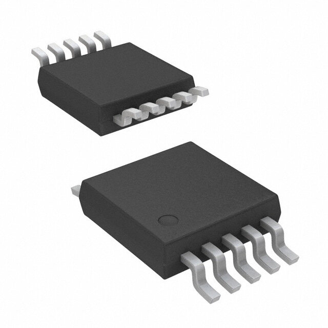
ICGOO在线商城 > 集成电路(IC) > PMIC - 稳压器 - 专用型 > EL7583IREZ
- 型号: EL7583IREZ
- 制造商: Intersil
- 库位|库存: xxxx|xxxx
- 要求:
| 数量阶梯 | 香港交货 | 国内含税 |
| +xxxx | $xxxx | ¥xxxx |
查看当月历史价格
查看今年历史价格
EL7583IREZ产品简介:
ICGOO电子元器件商城为您提供EL7583IREZ由Intersil设计生产,在icgoo商城现货销售,并且可以通过原厂、代理商等渠道进行代购。 EL7583IREZ价格参考。IntersilEL7583IREZ封装/规格:PMIC - 稳压器 - 专用型, - Converter, TFT LCD Voltage Regulator IC 2 Output 20-HTSSOP。您可以下载EL7583IREZ参考资料、Datasheet数据手册功能说明书,资料中有EL7583IREZ 详细功能的应用电路图电压和使用方法及教程。
| 参数 | 数值 |
| 产品目录 | 集成电路 (IC) |
| 描述 | IC CONV DC/DC 3CHN 20-HTSSOP |
| 产品分类 | |
| 品牌 | Intersil |
| 数据手册 | |
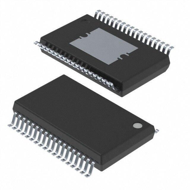
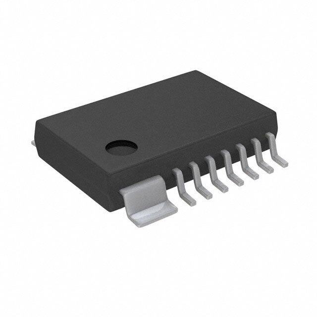
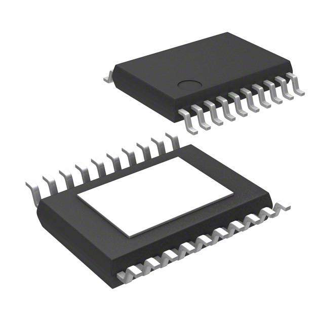
| 产品图片 |
|
| 产品型号 | EL7583IREZ |
| rohs | 无铅 / 符合限制有害物质指令(RoHS)规范要求 |
| 产品系列 | - |
| 供应商器件封装 | 20-HTSSOP |
| 包装 | 管件 |
| 安装类型 | 表面贴装 |
| 封装/外壳 | 20-TSSOP(0.173",4.40mm 宽)裸焊盘 |
| 工作温度 | -40°C ~ 85°C |
| 应用 | 转换器,TFT,LCD |
| 标准包装 | 74 |
| 电压-输入 | 2.7 V ~ 14 V |
| 电压-输出 | 5 V ~ 17 V |
| 输出数 | 2 |


PDF Datasheet 数据手册内容提取
DATASHEET EL7583 FN7335 3-Channel DC/DC Converter Rev 5.00 May 12, 2006 3-Channel DC/DC Converter Features The EL7583 is a 3-channel DC/DC converter IC which is • TFT-LCD display supply designed primarily for use in TFT-LCD applications. It - Boost regulator features a PWM boost converter with 2.7V to 14V input - VON charge pump capability and 5V to 17V output, which powers the column - VOFF charge pump drivers and provides up to 470mA @ 12V, 370mA @ 15V from 5V supply. A pair of charge pump control circuits • 2.7V to 14V VIN supply provide regulated outputs of VON and VOFF supplies at 8V • 5V < VBOOST < 17V to 40V and -5V to -40V, respectively, each at up to 60mA. • 5V < VON < 40V The EL7583 features adjustable switching frequency, • -40V < VOFF < 0V adjustable soft start, and a separate output VON enable control to allow selection of supply start-up sequence. An • VBOOST = 12V @ 470mA over-temperature feature is provided to allow the IC to be • VBOOST = 15V @ 370mA automatically protected from excessive power dissipation. • High frequency, small inductor DC/DC boost circuit The EL7583 is available in a standard 20 Ld TSSOP • Over 90% efficient DC/DC boost converter capability package and the Pb-free 20 Ld HTSSOP package. Both are specified for operation over the full -40°C to +85°C • Adjustable frequency temperature range. • Adjustable soft-start Ordering Information • Adjustable outputs PART PART TAPE & PKG. • Small parts count NUMBER MARKING REEL PACKAGE DWG. # • Pb-free plus anneal available (RoHS compliant) EL7583IR 7583IR - 20 Ld TSSOP MDP0044 Applications EL7583IR-T7 7583IR 7” 20 Ld TSSOP MDP0044 EL7583IR-T13 7583IR 13” 20 Ld TSSOP MDP0044 • TFT-LCD panels EL7583IREZ 7583IREZ - 20 Ld HTSSOP MDP0048 • PDAs (See Note) (Pb-free) Pinout EL7583IREZ-T7 7583IREZ 7” 20 Ld HTSSOP MDP0048 (See Note) (Pb-free) EL7583 (20 LD TSSOP/HTSSOP) EL7583IREZ-T13 7583IREZ 13” 20 Ld HTSSOP MDP0048 TOP VIEW (See Note) (Pb-free) NOTE: Intersil Pb-free plus anneal products employ special Pb-free VSSB 1 20ROSC material sets; molding compounds/die attach materials and 100% matte tin plate termination finish, which are RoHS compliant and SS 2 19ENP compatible with both SnPb and Pb-free soldering operations. Intersil FBB 3 18ENBN Pb-free products are MSL classified at Pb-free peak reflow temperatures that meet or exceed the Pb-free requirements of VDDB 4 17VREF IPC/JEDEC J STD-020. LX 5 16PGND LX 6 15PGND LX 7 14DRVP DRVN 8 13VDDP VDDN 9 12FBP FBN10 11VSSP REFER TO PCB LAYOUT GUIDELINE FN7335 Rev 5.00 Page 1 of 16 May 12, 2006
EL7583 Absolute Maximum Ratings (TA = 25°C) VIN Input Voltage . . . . . . . . . . . . . . . . . . . . . . . . . . . . . . . . . . . .14V Storage Temperature. . . . . . . . . . . . . . . . . . . . . . . .-65°C to +150°C VDDB, VDDP, VDDN . . . . . . . . . . . . . . . . . . . . . . . . . . . . . . . . . . .18V Die Junction Temperature . . . . . . . . . . . . . . . . . . . . . . . . . . . .125°C LX Voltage . . . . . . . . . . . . . . . . . . . . . . . . . . . . . . . . . . . . . . . . . .18V Power Dissipation . . . . . . . . . . . . . . . . . . . . . . . . . . . . . See Curves Maximum Continuous Output Current. . . . . . . . . . . . . . . . . . . . 0.5A Operating Ambient Temperature . . . . . . . . . . . . . . . .-40°C to +85°C CAUTION: Stresses above those listed in “Absolute Maximum Ratings” may cause permanent damage to the device. This is a stress only rating and operation of the device at these or any other conditions above those indicated in the operational sections of this specification is not implied. IMPORTANT NOTE: All parameters having Min/Max specifications are guaranteed. Typ values are for information purposes only. Unless otherwise noted, all tests are at the specified temperature and are pulsed tests, therefore: TJ = TC = TA Electrical Specifications VIN = 3.3V, VBOOST = 12V, ROSC = 100k, TA = 25°C Unless Otherwise Specified PARAMETER DESCRIPTION CONDITIONS MIN TYP MAX UNIT DC/DC BOOST CONVERTER IQ1_B Quiescent Current - Shut-down ENBN = ENP = 0V 0.8 10 µA IQ2_B Quiescent Current - Switching ENBN = VDDB 4.8 8 mA V(FBB) Feedback Voltage 1.275 1.300 1.325 V VREF Reference Voltage 1.260 1.310 1.360 V VROSC Oscillator Set Voltage 1.260 1.325 1.390 V I(FBB) Feedback Input Bias Current 0.1 µA VDDB Boost Converter Supply Range 2.7 17 V DMAX Maximum Duty Cycle 85 92 % I(LX)MAX Peak Internal FET Current 1.75 A RDS-ON Switch On Resistance at VBOOST = 10V, I(LX) total = 350mA 0.22 ILEAK-SWITCH Switch Leakage Current I(LX) total 1 µA VBOOST Output Range VBOOST > VIN + VDIODE 5 17 V VBOOST/VIN Line Regulation 2.7V < VIN < 13.2V, VBOOST = 15V 0.1 % VBOOST/IO1 Load Regulation 50mA < IO1 < 250mA 0.5 % FOSC-RANGE Frequency Range ROSC range = 240k to 60k 200 1000 kHz FOSC1 Switching Frequency ROSC = 100k 620 680 750 kHz POSITIVE REGULATED CHARGE PUMP (VON) Most positive VON output depends on the magnitude of the VDDP input voltage (normally connected to VBOOST) and the external component configuration (doubler or tripler) VDDP Supply Input for Positive Charge Pump Usually connected to VBOOST output 5 17 V IQ1(VDDP) Quiescent Current - Shut-down ENP = 0V 11.5 20 µA IQ2(VDDP) Quiescent Current - Switching ENBN = ENP = VDDB 2.3 5 mA V(FBP) Feedback Reference Voltage 1.245 1.310 1.375 V I(FBP) Feedback Input Bias Current 0.1 µA I(DRVP) RMS DRVP Output Current VDDP = 12V 60 mA VDDP = 6V 15 mA ILR_VON Load Regulation 5mA < IL < 15mA -0.5 0.03 0.5 %/mA FPUMP Charge Pump Frequency Frequency set by ROSC - see boost section 0.5*FOSC FN7335 Rev 5.00 Page 2 of 16 May 12, 2006
EL7583 Electrical Specifications VIN = 3.3V, VBOOST = 12V, ROSC = 100k, TA = 25°C Unless Otherwise Specified (Continued) PARAMETER DESCRIPTION CONDITIONS MIN TYP MAX UNIT NEGATIVE REGULATED CHARGE PUMP (VOFF) Most negative VOFF output depends on the magnitude of the VDDN input voltage (normally connected to VBOOST) and the external component configuration (doubler or tripler) VDDN Supply Input for Negative Charge Pump Usually connected to VBOOST output 5 17 V IQ1(VDDN) Quiescent Current - Shut-down ENBN = 0V 1.2 10 µA IQ2(VDDN) Quiescent Current - Switching ENBN = VDDB 2.3 5 mA V(FBN) Feedback Reference Voltage -80 0 +80 mV I(FBN) Feedback Input Bias Current Magnitude of input bias 0.1 µA I(DRVN) RMS DRVN Output Current VDDN = 12V 60 mA VDDN = 6V 15 mA ILR_VOFF Load Regulation -15mA < IL < -5mA -0.5 0.03 0.5 %/mA FPUMP Charge Pump Frequency Frequency set by ROSC - see boost section 0.5*FOSC ENABLE CONTROL LOGIC VHI-ENX Enable Input High Threshold x = “BN”, “P” 1.6 V VLO-ENX Enable Input Low Threshold x = “BN”, “P” 0.8 V IL(EN”X”) Logic Low Bias Current X = “BN”, “P” = 0V 0.1 µA IL(ENBN) Logic High Bias Current ENBN = 5V 7.5 15 µA IL(ENP) Logic High Bias Current ENP = 5V 3.3 7.5 µA OVER-TEMPERATURE PROTECTION TOT Over-temperature Threshold 130 °C THYS Over-temperature Hysteresis 40 °C FN7335 Rev 5.00 Page 3 of 16 May 12, 2006
EL7583 Pin Descriptions I = Input, O = Output, S = Supply PIN NUMBER PIN NAME PIN TYPE PIN FUNCTION 1 VSSB S Ground for DC/DC boost and reference circuits; chip substrate 2 SS I Soft-start input; the capacitor connected to this pin sets the current limited start time 3 FBB I Voltage feedback input for boost circuit; determines boost output voltage, VBOOST 4 VDDB S Positive supply input for DC/DC boost circuits 5 LX O Boost regulator inductor drive connected to drain of internal NFET 6 LX O Boost regulator inductor drive connected to drain of internal NFET 7 LX O Boost regulator inductor drive connected to drain of internal NFET 8 DRVN O Driver output for the external generation of negative charge pump voltage, VOFF 9 VDDN S Positive supply for input for VOFF generator 10 FBN I Voltage feedback input to determine negative charge pump output, VOFF 11 VSSP S Negative supply pin for both the positive and negative charge pumps 12 FBP I Voltage feedback to determine positive charge pump output, VON 13 VDDP S Positive supply input for VON generator 14 DRVP O Voltage driver output for the external generation of positive charge pump, VON 15 PGND O Power ground, connected to source of internal NFET 16 PGND O Power ground, connected to source of internal NFET 17 VREF I Voltage reference for charge pump circuits; decouple to ground 18 ENBN I Enable pin for boost (VBOOST generation) and negative charge pump (VOFF generation); active high 19 ENP I Enable for DRVP (VON generation); active high 20 ROSC I Connected to an external resistor to ground; sets the switching frequency of the DC/DC boost FN7335 Rev 5.00 Page 4 of 16 May 12, 2006
EL7583 Typical Performance Curves 95 95 90 90 9V 5V 85 9V 12V 85 15V %) 80 12V %) CY ( 75 15V CY ( 80 N N E E CI 70 CI 75 FI FI F 65 F E E 70 60 55 VIN=3.3V 65 VIN=5V FREQ=1MHz FREQ=1MHz 50 60 0 100 200 300 400 500 600 700 800 0 100 200 300 400 500 600 700 800 IOUT (mA) IOUT (mA) FIGURE 1. EFFICIENCY vs IOUT FIGURE 2. EFFICIENCY vs IOUT 95 95 90 90 5V 15V 12V 9V 85 85 %) 9V %) Y ( 80 15V 12V Y ( 80 C C N N E E CI 75 CI 75 FI FI F F E 70 E 70 65 VIN=3.3V 65 VIN=5V FREQ=700kHz FREQ=700kHz 60 60 0 100 200 300 400 500 600 700 800 0 100 200 300 400 500 600 700 800 IOUT (mA) IOUT (mA) FIGURE 3. EFFICIENCY vs IOUT FIGURE 4. EFFICIENCY vs IOUT 970 1.27 969 ROSC = 61.9k 968 1.265 z) kH 967 V) Y ( E ( NC 966 AG 1.26 E T U L Q 965 O E V R F 964 1.255 963 962 1.25 3 3.5 4 4.5 5 5.5 6 -50 0 50 100 150 VDDB (V) TEMPERATURE (°C) FIGURE 5. FS vs VDDB FIGURE 6. VREF vs TEMPERATURE FN7335 Rev 5.00 Page 5 of 16 May 12, 2006
EL7583 Typical Performance Curves (Continued) f=675kHz, VIN=5.0V f=675kHz, VIN=3.3V 1.5 1.5 1.0 1.0 %) %) ON ( 0.5 ON ( 0.5 TI TI A A UL 0.0 UL 0.0 G G E E R R D -0.5 D -0.5 A A O O 15V L L -1.0 -1.0 12V 12V 9V 18V 9V 5V 18V 15V -1.5 -1.5 0 100 200 300 400 500 600 700 0 100 200 300 400 500 600 700 800 IOUT (mA) IOUT (mA) FIGURE 7. LOAD REGULATION vs IOUT FIGURE 8. LOAD REGULATION vs IOUT f=1MHz, VIN=5.0V f=1MHz, VIN=3.3V 1.5 1.5 1.0 1.0 %) %) ON ( 0.5 ON ( 0.5 ATI ATI UL 0.0 UL 0.0 G G E E R R D -0.5 D -0.5 A A LO LO 15V 12V -1.0 18V 12V 9V -1.0 9V 15V 18V 5V -1.5 -1.5 0 100 200 300 400 500 600 700 0 100 200 300 400 500 600 700 800 IOUT (mA) IOUT (mA) FIGURE 9. LOAD REGULATION vs IOUT FIGURE 10. LOAD REGULATION vs IOUT 20 6.5 19 VDDP = 15V 6 VDDN = 15V VDDN = 12V 18 5.5 VDDP = 12V V) V) (ON 17 (-FF 5 V O 16 V 4.5 15 4 14 3.5 0 10 20 30 40 50 60 70 80 0 10 20 30 40 50 60 70 80 ILOAD (mA) ILOAD (mA) FIGURE 11. VON vs ION FIGURE 12. VOFF vs IOFF FN7335 Rev 5.00 Page 6 of 16 May 12, 2006
EL7583 Typical Performance Curves (Continued) f(MHz)=1/(0.0118 ROSC+0.378) SWITCHING PERIOD(µs)=0.0118 ROSC+0.378) 1400 6 1200 5 s) µ Hz) 1000 OD ( 4 Y (k 800 ERI C P 3 N G QUE 600 HIN E C 2 FR 400 WIT S 1 200 0 0 0 50 100 150 200 250 300 350 400 450 0 50 100 150 200 250 300 350 400 450 ROSC (k) ROSC (k) FIGURE 13. FS vs ROSC FIGURE 14. FS vs ROSC 100K & 0.1µF DELAY NETWORK ON ENP, CSS=0.1µF 100K & 0.1µF DELAY NETWORK ON ENP, CSS=0.1µF VBOOST VBOOST 5V/DIV 5V/DIV 10V/DIV VON VON 10V/DIV 2V/DIV VOFF 2V/DIV VOFF 200ms/DIV 11mmss//DDIIVV FIGURE 15. POWER-DOWN FIGURE 16. POWER-UP VIN=3.3V, VOUT=11.3V, IOUT=50mA VIN=3.3V, VOUT=11.3V, IOUT=250mA FIGURE 17. LX WAVEFORM - DISCONTINUOUS MODE FIGURE 18. LX WAVEFORM - CONTINUOUS MODE FN7335 Rev 5.00 Page 7 of 16 May 12, 2006
EL7583 Typical Performance Curves (Continued) JEDEC JESD51-7 HIGH EFFECTIVE THERMAL CONDUCTIVITY TEST BOARD HTSSOP EXPOSED DIEPAD SOLDERED TO PCB JEDEC JESD51-3 LOW EFFECTIVE THERMAL PER JESD51-5 CONDUCTIVITY TEST BOARD 3.5 1 3 2.857W 0.9 800mW W) W) 0.8 N ( 2.5 HTSSOP20 N ( 0.7 HTSSOP20 O O 714mW ATI 2 JA=35°C/W ATI 0.6 JA = 125°C/W P P SI SI 0.5 TSSOP20 R DIS 1.5 R DIS 0.4 JA=140°C/W WE 1 1.111W WE 0.3 PO TSSOP20 PO 0.2 0.5 0.1 JA=90°C/W 0 0 0 25 50 75 85 100 125 150 0 25 50 75 85 100 125 150 AMBIENT TEMPERATURE (°C) AMBIENT TEMPERATURE (°C) FIGURE 19. PACKAGE POWER DISSIPATION vs AMBIENT FIGURE 20. PACKAGE POWER DISSIPATION vs AMBIENT TEMPERATURE TEMPERATURE Functional Block Diagram VOUT R2 10µH VIN R1 110k 49 13k 10µF 10µF 0.1µF FBB VDDB LX MAX_DUTY ROSC R3 REFERENCE 62k GENERATOR VREF PWM PWM VRAMP COMPARATOR LOGIC 0.22 ENBN 12µA START-UP - OSCILLATOR + ILOUT 7.2K 160m VSSB SS PGND 0.1µF FN7335 Rev 5.00 Page 8 of 16 May 12, 2006
EL7583 Applications Information Steady-State Operation The EL7583 is high efficiency multiple output power solution When the output reaches the preset voltage, the regulator designed specifically for thin-film transistor (TFT) liquid operates at steady state. Depending on the input/output crystal display (LCD) applications. The device contains one condition and component, the inductor operates at either high current boost converter and two low power charge continuous-conduction mode or discontinuous-conduction pumps (VON and VOFF). mode. The boost converter contains an integrated N-channel In the continuous-conduction mode, the inductor current is a MOSFET to minimize the number of external components. triangular waveform and LX voltage a pulse waveform. In the The converter output voltage can be set from 5V to 18V with discontinuous-conduction mode, the inductor current is external resistors. The VON and VOFF charge pumps are completely ‘dried-out’ before the MOSFET is turned on independently regulated to positive and negative voltages again. The input voltage source, the inductor, and the using external resistors. Output voltages as high as 40V can MOSFET and output diode parasitic capacitors forms a be achieved with additional capacitors and diodes. resonant circuit. Oscillation will occur in this period. This oscillation is normal and will not affect the regulation. Boost Converter At very low load, the MOSFET will skip pulse sometimes. The boost converter operates in constant frequency pulse- This is normal. width-modulation (PWM) mode. Quiescent current for the EL7583 is only 5mA when enabled, and since only the low Current Limit side MOSFET is used, switch drive current is minimized. The MOSFET current limit is nominal ILMT = 1.75. This 90% efficiency is achieved in most common application restricts the maximum output current IOMAX based on the operating conditions. following formula: A functional block diagram with typical circuit configuration is shown on previous page. Regulation is performed by the I = I –-----L--V-----I--N-- OMAX LMT 2 V O PWM comparator which regulates the output voltage by comparing a divided output voltage with an internal where: reference voltage. The PWM comparator outputs its result to the PWM logic. The PWM logic switches the MOSFET on • IL is the inductor peak-to-peak current ripple and is decided by: and off through the gate drive circuit. Its switching frequency is external adjustable with a resistor from timing control pin I = V-----I--N----D----- (ROSC) to ground. The boost converter has 200kHz to L L FS 1.2MHz operating frequency range. Start-Up • D is the MOSFET turn-on radio and is decided by: After VDDB reaches a threshold of about 2V, the power D = V-----O---- ----- --V----I--N--- MOSFET is controlled by the start-up oscillator, which V O generates fixed duty-ratio of 0.5 - 0.7 at a frequency of several hundred kilohertz. This will boost the output voltage, • FS is the switching frequency. providing the initial output current load is not too great (<250mA). When VDDB reaches about 3.7V, the PWM comparator takes over the control. The duty ratio will be decided by the multiple-input direct summing comparator, Max_Duty signal (about 90% duty-ratio), and the Current Limit Comparator, whichever is the smallest. The soft-start is provided by the current limit comparator. As the internal 12µA current source charges the external soft- start capacitor, the peak MOSFET current is limited by the voltage on the capacitor. This in turn controls the rising rate of output voltage. The regulator goes through the start-up sequence as well after the ENBN signal is pulled to HI. FN7335 Rev 5.00 Page 9 of 16 May 12, 2006
EL7583 The following table gives typical values: A 1nF compensation capacitor across the feedback resistor (Margins are considered 10%, 3%, 20%, 10%, and 15% on to ground is recommended to keep the converter in stable VIN, VO, L, FS, and ILMT, respectively) operation at low output current and high frequency conditions. TABLE 1. MAXIMUM CONTINUOUS OUTPUT CURRENT Schottky Diode VIN (V) VO (V) L (ΜH) FS (kHz) IOMAX (mA) Speed, forward voltage drop, and reverse current are the 3.3 9 10 1000 430 three most critical specifications for selecting the Schottky 3.3 12 10 1000 320 diode. The entire output current flows through the diode, so 3.3 15 10 1000 250 the diode average current is the same as the average load current and the peak current is the same as the inductor 5 9 10 1000 650 peak current. When selecting the diode, one must consider 5 12 10 1000 470 the forward voltage drop at the peak diode current. On the 5 15 10 1000 370 Elantec demo board, MBRM120 is selected. Its forward voltage drop is 450mV at 1A forward current. 12 18 10 1000 830 Output Capacitor Component Considerations The EL7583 is specially compensated to be stable with Input Capacitor capacitors which have a worst-case minimum value of 10µF at the particular VOUT being set. Output ripple voltage It is recommended that CIN is larger than 10µF. requirements also determine the minimum value and the Theoretically, the input capacitor has ripple current of IL. type of capacitors. Output ripple voltage consists of two Due to high-frequency noise in the circuit, the input current components - the voltage drop caused by the switching ripple may exceed the theoretical value. Larger capacitor will current though the ESR of the output capacitor and the reduce the ripple further. charging and discharging of the output capacitor: Boost Inductor V - V I The inductor has peak and average current decided by: V = I ESR+-----O----U----T--------------I--N--------------O----U-----T---------- RIPPLE LPK V C FS OUT OUT I I = I +-------L- LPK LAVG 2 For low ESR ceramic capacitors, the output ripple is I I = ------O------- dominated by the charging/discharging of the output LAVG 1 - D capacitor. The inductor should be chosen to be able to handle this In addition to the voltage rating, the output capacitor should current. Furthermore, due to the fixed internal also be able to handle the RMS current is given by: compensation, it is recommended that maximum inductance oofu 1tp0uµt Hv oaltnadg e1,5 rµeHs ptoe cbtiev eulsye.d in the 5V and 12V or higher ICORMS = 1 - DD+---------I--L---2----2--1--1--2--ILAVG ILAVG The output diode has average current of IO, and peak current the same as the inductor's peak current. Schottky diode is Positive and Negative Charge Pump (V and ON recommended and it should be able to handle those currents. V ) OFF Feedback Resistor Network The EL7583 contains two independent charge pumps (see charge pump block and connection diagram.) The negative An external resistor divider is required to divide the output voltage down to the nominal reference voltage. Current charge pump inverts the VDDN supply voltage and provides a regulated negative output voltage. The positive charge drawn by the resistor network should be limited to maintain the overall converter efficiency. The maximum value of the pump doubles the VDDP supply voltage and provides a regulated positive output voltage. The regulation of both the resistor network is limited by the feedback input bias current negative and positive charge pumps is generated by the and the potential for noise being coupled into the feedback internal comparator that senses the output voltage and pin. A resistor network in the order of 200k is compares it with and internal reference. The switching recommended. The boost converter output voltage is frequency of the charge pump is set to ½ the boost converter determined by the following relationship: switching frequency. R +R V = -----1--------------2--V The pumps use pulse width modulation to adjust the pump BOOST R FBB 1 period, depending on the load present. The pumps are short- circuit protected to 180mA at 12V supply and can provide where VFBB is 1.300V. 15mA to 60mA for 6V to 12V supply. FN7335 Rev 5.00 Page 10 of 16 May 12, 2006
EL7583 Single Stage Charge Pump VDDN 5V TO VDDP 17V 5V TO 0.1µF 17V RONP RONP 0.1µF CCPP DRVN OSC DRVP CCPN VOFF COUT2 RONN RONN COUTV1ON 3.3µF VSSN VSSP R12 2.2µF R21 FBN FBP + - - + + - VFBP R11 RON IS 30 - 40 FOR VDD 6V TO 12V R22 VREF Positive Charge Pump Design Considerations A single stage charge pump is shown above. The maximum VON output voltage is determined by the following equation: 1 1 V max2V - I 2R +R - 2V - I -------------------------------------------- - I ------------------------------------------------ ON DDCPP OUT ONN ONP DIODE OUT 0.5F C OUT 0.5F C S CPP S OUT1 where: • RONN and RONP resistance values depend on the VDDP voltage levels. For 12V supply, RON is typically 33. For 6V supply, RON is typically 45. If additional stage is required, the LX switching signal is recommended to drive the additional charge pump diodes. The drive impedance at the LX switching is typically 220m. The figure below illustrates an implementation for two-stage positive charge pump circuit. FN7335 Rev 5.00 Page 11 of 16 May 12, 2006
EL7583 Two-Stage Positive Charge Pump Circuit VDDP V(5BVO-1O7SVT) VLX RONP CCPP DRNP VON CCPP RONN COUT1 COUT1 VSSP R12 FBP - + + 1.265V - R11 The maximum VON output voltage for N+1 stage charge pump is: 1 V max2V - I 2R +R - 2V - I -------------------------------------------- - I ON DDP OUT ONN ONP DIODE OUT 0.5F C OUT S CPP -----------------------1-------------------------+NV max - N2V +I ---------------------1-----------------------+I -----------------------1------------------------- 0.5F C LX DIODE OUT 0.5F C OUT 0.5F C S OUT1 S CPP S OUT1 R11 and R12 set the VON output voltage: R +R V = V -----1---1--------------1---2-- ON FBP R 11 where VFBP is 1.310V. Negative Charge Pump Design Considerations The criteria for the negative charge pump is similar to the positive charge pump. For a single stage charge pump, the maximum VOFF output voltage is: 1 1 V maxI 2R +R +2V - I -------------------------------------------- - I ------------------------------------------------ - V OFF OUT ONN ONP DIODE OUT 0.5F C OUT 0.5F C DDN S CPN S OUT2 Similar to positive charge pump, if additional stage is required, the LX switching signal is recommended to drive the additional charge pump diodes. The figure on the next page shows a two stage negative charge pump circuit. FN7335 Rev 5.00 Page 12 of 16 May 12, 2006
EL7583 Two-Stage Negative Charge Pump Circuit VDDN 5V-17V VLX RONP CCPN DRVN VOFF CCPN RONN COUT2 COUT2 VSSN R21 FBN + - R22 VREF The maximum VOFF output voltage for N+1 stage charge pump is: 1 1 V maxI 2R +R +2V - I -------------------------------------------- - I ------------------------------------------------ - OFF OUT ONN ONP DIODE OUT 0.5F C OUT 0.5F C S CPN S OUT2 V - NV max+N2V +I ---------------------1-----------------------+I -----------------------1------------------------- DDN LX DIODE OUT 0.5F C OUT 0.5F C S CPN S OUT2 R21 and R22 determine VOFF output voltage: R V = -V -----2---1-- OFF REF R 22 where VREF is 1.310V. Over-Temperature Protection An internal temperature sensor continuously monitors the shielding trace or layer. This is to prevent undesirable die temperature. In the event that die temperature exceeds switching interactions coupling into the feedback inputs. the thermal trip point, the device will shut down and disable • Place the charge pump feedback resistor network after the itself. The upper and lower trip points are typically set to diode and output capacitor node to avoid switching noise. 130°C and 90°C respectively. • All low-side feedback resistors should be connected PCB Layout Guidelines directly to VSSB. VSSB should be connected to the power Careful layout is critical in the successful operation of the ground close at one point only. application. The following layout guidelines are A demo board is available to illustrate the proper layout recommended to achieve optimum performance. implementation. • VREF and VDDB bypass capacitors should be placed next to the pins. • Place the boost converter diode and inductor close to the LX pins. • Place the boost converter output capacitor close to the PGND pins. • Locate feedback dividers close to their respected feedback pins to avoid switching noise coupling into the high impedance node. • Switching output PCB traces should not cross, or be laid out adjacent to, feedback traces without using a grounded FN7335 Rev 5.00 Page 13 of 16 May 12, 2006
EL7583 Typical Application Circuit R2 R3 110K 1 VSSB ROSC 20 C7 61.9K C10 2 SS ENP 19 R5 497K 0.1µF R6 0 OPEN13RK1 R4 3 FBB ENBN 18 C8 C50 0.1µF OPEN 49.9 C6 4 VDDB VREF 17 VB(1O2OVS@T C5 + C4 C3 D1* 0.1µF 5 LX PGND 16 C9 500mA) 10µF OPEN 22µF 6 LX PGND 15 1nF L1 C12 0.1µF VIN C1 + C2 10µH C22 7 LX DRVP 14 D11** (18VV@O1N8mA) 10µF 4.7µF VOFF GND 0.1µF 8 DRVN VDDP 13 C11 1(-56mV@A) C21 9 VDDN FBP 12 0.1µF C0.116µF C2.127µF R511K2 R21 C27 C26 0.1µF 10 FBN VSSP 11 154K 0.1µF 3.3µF R11 3.9K D21** R22 33.2K * MBRM120LT3 ** BAT54S FN7335 Rev 5.00 Page 14 of 16 May 12, 2006
EL7583 TSSOP Package Outline Drawing FN7335 Rev 5.00 Page 15 of 16 May 12, 2006
EL7583 HTSSOP Package Outline Drawing NOTE: The package drawing shown here may not be the latest version. To check the latest revision, please refer to the Intersil website at http://www.intersil.com/design/packages/index.asp © Copyright Intersil Americas LLC 2003-2006. All Rights Reserved. All trademarks and registered trademarks are the property of their respective owners. For additional products, see www.intersil.com/en/products.html Intersil products are manufactured, assembled and tested utilizing ISO9001 quality systems as noted in the quality certifications found at www.intersil.com/en/support/qualandreliability.html Intersil products are sold by description only. Intersil may modify the circuit design and/or specifications of products at any time without notice, provided that such modification does not, in Intersil's sole judgment, affect the form, fit or function of the product. Accordingly, the reader is cautioned to verify that datasheets are current before placing orders. Information furnished by Intersil is believed to be accurate and reliable. However, no responsibility is assumed by Intersil or its subsidiaries for its use; nor for any infringements of patents or other rights of third parties which may result from its use. No license is granted by implication or otherwise under any patent or patent rights of Intersil or its subsidiaries. For information regarding Intersil Corporation and its products, see www.intersil.com FN7335 Rev 5.00 Page 16 of 16 May 12, 2006
 Datasheet下载


