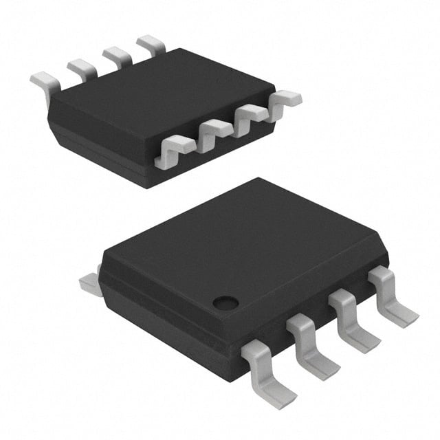
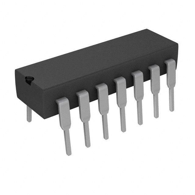
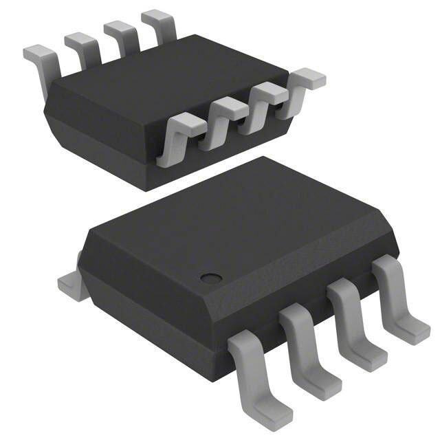
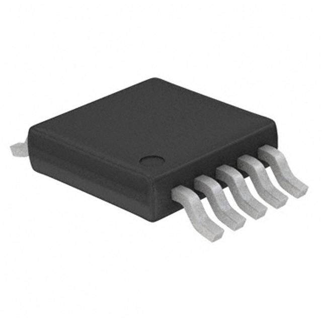
ICGOO在线商城 > 集成电路(IC) > 线性 - 放大器 - 仪表,运算放大器,缓冲器放大器 > EL5104ISZ
- 型号: EL5104ISZ
- 制造商: Intersil
- 库位|库存: xxxx|xxxx
- 要求:
| 数量阶梯 | 香港交货 | 国内含税 |
| +xxxx | $xxxx | ¥xxxx |
查看当月历史价格
查看今年历史价格
EL5104ISZ产品简介:
ICGOO电子元器件商城为您提供EL5104ISZ由Intersil设计生产,在icgoo商城现货销售,并且可以通过原厂、代理商等渠道进行代购。 EL5104ISZ价格参考。IntersilEL5104ISZ封装/规格:线性 - 放大器 - 仪表,运算放大器,缓冲器放大器, 电压反馈 放大器 1 电路 8-SOIC。您可以下载EL5104ISZ参考资料、Datasheet数据手册功能说明书,资料中有EL5104ISZ 详细功能的应用电路图电压和使用方法及教程。
| 参数 | 数值 |
| -3db带宽 | 700MHz |
| 产品目录 | 集成电路 (IC) |
| 描述 | IC OPAMP VFB 700MHZ 8SOIC |
| 产品分类 | Linear - Amplifiers - Instrumentation, OP Amps, Buffer Amps |
| 品牌 | Intersil |
| 数据手册 | |
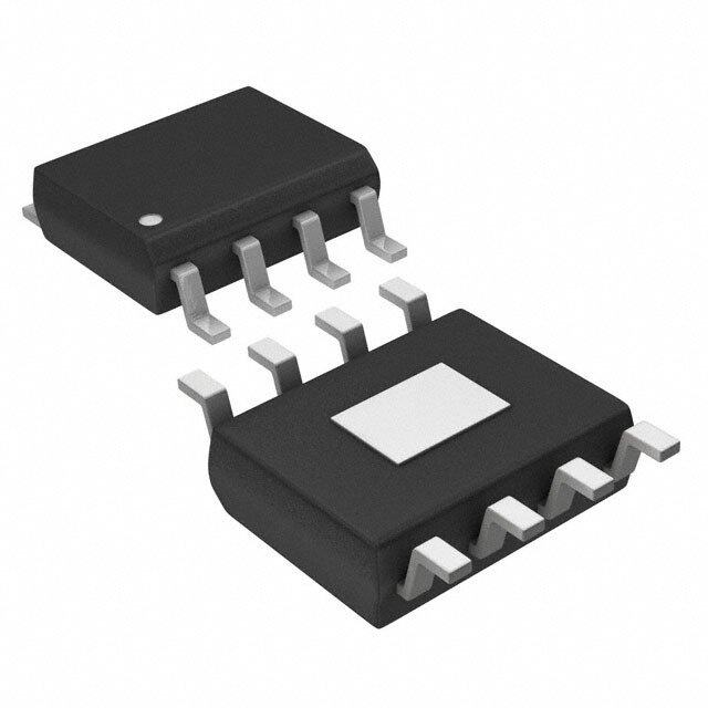
| 产品图片 |
|
| 产品型号 | EL5104ISZ |
| PCN组件/产地 | |
| rohs | 无铅 / 符合限制有害物质指令(RoHS)规范要求 |
| 产品系列 | - |
| 产品培训模块 | http://www.digikey.cn/PTM/IndividualPTM.page?site=cn&lang=zhs&ptm=4278 |
| 产品目录页面 | |
| 供应商器件封装 | 8-SOIC |
| 包装 | 管件 |
| 压摆率 | 3000 V/µs |
| 增益带宽积 | - |
| 安装类型 | 表面贴装 |
| 封装/外壳 | 8-SOIC(0.154",3.90mm 宽) |
| 工作温度 | -40°C ~ 85°C |
| 放大器类型 | 电压反馈 |
| 标准包装 | 97 |
| 电压-电源,单/双 (±) | 4 V ~ 13.2 V, ±2 V ~ 6.6 V |
| 电压-输入失调 | 3mV |
| 电流-电源 | 9.5mA |
| 电流-输入偏置 | 8µA |
| 电流-输出/通道 | 160mA |
| 电路数 | 1 |
| 输出类型 | - |




- 商务部:美国ITC正式对集成电路等产品启动337调查
- 曝三星4nm工艺存在良率问题 高通将骁龙8 Gen1或转产台积电
- 太阳诱电将投资9.5亿元在常州建新厂生产MLCC 预计2023年完工
- 英特尔发布欧洲新工厂建设计划 深化IDM 2.0 战略
- 台积电先进制程称霸业界 有大客户加持明年业绩稳了
- 达到5530亿美元!SIA预计今年全球半导体销售额将创下新高
- 英特尔拟将自动驾驶子公司Mobileye上市 估值或超500亿美元
- 三星加码芯片和SET,合并消费电子和移动部门,撤换高东真等 CEO
- 三星电子宣布重大人事变动 还合并消费电子和移动部门
- 海关总署:前11个月进口集成电路产品价值2.52万亿元 增长14.8%


PDF Datasheet 数据手册内容提取
DATASHEET EL5104, EL5105, EL5204, EL5205, EL5304 FN7332 700MHz Slew-Enhanced VFAs Rev 8.00 May 25, 2016 The EL5104, EL5105, EL5204, EL5205, and EL5304 Features represent high speed voltage feedback amplifiers based on • Specified for 5V or ±5V applications the current feedback amplifier architecture. This gives the typical high slew rate benefits of a CFA family along with the • Power-down to 17µA stability and ease of use associated with the VFA type • -3dB bandwidth = 700MHz architecture. This family is available in single, dual, and triple versions, with 200MHz, 400MHz, and 700MHz versions. • ±0.1dB bandwidth = 45MHz This family operates on single 5V or ±5V supplies from • Low supply current = 9.5mA minimum supply current. The EL5104 and EL5204 also feature an output enable function, which can be used to put • Slew rate = 7000V/µs the output in to a high-impedance mode. This enables the • Low offset voltage = 10mV max outputs of multiple amplifiers to be tied together for use in • Output current = 160mA multiplexing applications. • AVOL = 1400 • Diff gain/phase = 0.01%/0.02° • Pb-free plus anneal available (RoHS compliant) Applications • Video amplifiers • PCMCIA applications • A/D drivers • Line drivers • Portable computers • High speed communications • RGB applications • Broadcast equipment • Active filtering FN7332 Rev 8.00 Page 1 of 18 May 25, 2016
EL5104, EL5105, EL5204, EL5205, EL5304 Pinouts EL5104 EL5104 EL5105 (6 LD SOT-23) (8 LD SOIC) (5 LD SOT-23, SC-70) TOP VIEW TOP VIEW TOP VIEW D E OUT 1 6 VS+ NC 1 8 ERNTABLE OUT 1 5 VS+ O UPP VINS+- 23 + - 45 EINN-ABLE IINN+- 23 +-A BLE O R S 76 VOSU+T VINS+- 23 + - 4 IN- AVAIL VS- 4 R 5 NC E G N O O L N EL5204 EL5205 EL5304 (10 LD MSOP) (8 LD SOIC, MSOP) (16 LD QSOP) TOP VIEW TOP VIEW TOP VIEW OUT 1 10VS+ OUTA 1 8 VS+ INA+ 1 16INA- D E IN- 2 9 OUT INA- 2 - 7 OUTB CEA 2 - 15OOURTTA VINS+- 34 +- +- 877 IINN-+ INVAS+- 34 + +- 65 IINNBB-+ CVESB- 34 AVAILA++-BLE O R S11U43PPVOSU+TB CE 5 6 CE INB+ 5 ER 12INB- G N O NOC L 6 11NC N + CEC 7 10OUTC - INC+ 8 9 INC- Ordering Information PART NUMBER PART MARKING TAPE & REEL PACKAGE PKG. DWG. # EL5104ISZ (Note) (No longer 5104ISZ - 8 Ld SOIC (150 mil) (Pb-Free) MDP0027 available, recommended replacement: EL5104IWZ-T7) EL5104ISZ-T7 (Note) (No longer 5104ISZ 7” 8 Ld SOIC (150 mil) (Pb-Free) MDP0027 available, recommended replacement: EL5104IWZ-T7) EL5104ISZ-T13 (Note) (No longer 5104ISZ 13” 8 Ld SOIC (150 mil) (Pb-Free) MDP0027 available, recommended replacement: EL5104IWZ-T7) EL5104IWZ-T7 (Note) BAEA 7” (3k pcs) 6 Ld SOT-23 (Pb-Free) P5.064A EL5104IWZ-T7A (Note) BAEA 7” (250 pcs) 6 Ld SOT-23 (Pb-Free) P5.064A EL5105IC (No longer available or C - 5 Ld SC-70 (1.25mm) P5.049 supported) EL5105IWZ-T7 (Note) BBMA 7” (3k pcs) 5 Ld SOT-23 (Pb-Free) P5.064A EL5105IWZ-T7A (Note) BBMA 7” (250 pcs) 5 Ld SOT-23 (Pb-Free) P5.064A EL5204IYZ (Note) BAAAF - 10 Ld MSOP (3.0mm) (Pb-Free) MDP0043 EL5204IYZ-T7 (Note) BAAAF 7” 10 Ld MSOP (3.0mm) (Pb-Free) MDP0043 EL5204IYZ-T13 (Note) BAAAF 13” 10 Ld MSOP (3.0mm) (Pb-Free) MDP0043 FN7332 Rev 8.00 Page 2 of 18 May 25, 2016
EL5104, EL5105, EL5204, EL5205, EL5304 Ordering Information (Continued) PART NUMBER PART MARKING TAPE & REEL PACKAGE PKG. DWG. # EL5205ISZ (Note) 5205ISZ - 8 Ld SOIC (150 mil) (Pb-Free) MDP0027 EL5205ISZ-T7 (Note) 5205ISZ 7” 8 Ld SOIC (150 mil) (Pb-Free) MDP0027 EL5205ISZ-T13 (Note) 5205ISZ 13” 8 Ld SOIC (150 mil) (Pb-Free) MDP0027 EL5304IU (No longer available or 5304IU - 16 Ld QSOP (150 mil) MDP0040 supported) EL5304IU-T7 (No longer available 5304IU 7” 16 Ld QSOP (150 mil) MDP0040 or supported) EL5304IU-T13 (No longer available 5304IU 13” 16 Ld QSOP (150 mil) MDP0040 or supported) EL5304IUZ (Note) (No longer 5304IUZ - 16 Ld QSOP (150 mil) (Pb-Free) MDP0040 available or supported) EL5304IUZ-T7 (Note) (No longer 5304IUZ 7” 16 Ld QSOP (150 mil) (Pb-Free) MDP0040 available or supported) EL5304IUZ-T13 (Note) (No longer 5304IUZ 13” 16 Ld QSOP (150 mil) (Pb-Free) MDP0040 available or supported) NOTE: Intersil Pb-free plus anneal products employ special Pb-free material sets; molding compounds/die attach materials and 100% matte tin plate termination finish, which are RoHS compliant and compatible with both SnPb and Pb-free soldering operations. Intersil Pb-free products are MSL classified at Pb-free peak reflow temperatures that meet or exceed the Pb-free requirements of IPC/JEDEC J STD-020. FN7332 Rev 8.00 Page 3 of 18 May 25, 2016
EL5104, EL5105, EL5204, EL5205, EL5304 Absolute Maximum Ratings (TA = +25°C) Thermal Information Supply Voltage between VS+ and GND. . . . . . . . . . . . . . . . . . 13.2V Storage Temperature Range . . . . . . . . . . . . . . . . . .-65°C to +150°C Input Voltage . . . . . . . . . . . . . . . . . . . . . . . . . . . . . . . . . . . . . . . .±VS Ambient Operating Temperature Range . . . . . . . . . .-40°C to +85°C Differential Input Voltage . . . . . . . . . . . . . . . . . . . . . . . . . . . . . . .±4V Operating Junction Temperature. . . . . . . . . . . . . . . . . . . . . .+150°C Maximum Output Current. . . . . . . . . . . . . . . . . . . . . . . . . . . . . 80mA Pb-free reflow profile . . . . . . . . . . . . . . . . . . . . . . . . . .see link below VS+ to VS- Maximum Slew Rate . . . . . . . . . . . . . . . . . . . . . . . 1V/µs http://www.intersil.com/pbfree/Pb-FreeReflow.asp CAUTION: Stresses above those listed in “Absolute Maximum Ratings” may cause permanent damage to the device. This is a stress only rating and operation of the device at these or any other conditions above those indicated in the operational sections of this specification is not implied. IMPORTANT NOTE: All parameters having Min/Max specifications are guaranteed. Typical values are for information purposes only. Unless otherwise noted, all tests are at the specified temperature and are pulsed tests, therefore: TJ = TC = TA DC Electrical Specifications VS = ±5V, GND = 0V, TA = +25°C, VCM = 0V, VOUT = 0V, VENABLE = GND or OPEN, Unless Otherwise Specified. PARAMETER DESCRIPTION CONDITIONS MIN TYP MAX UNIT VOS Offset Voltage EL5104, EL5105, EL5204, EL5205 -10 3 10 mV EL5304 -18 5 18 mV TCVOS Offset Voltage Temperature Coefficient Measured from TMIN to TMAX 10 µV/°C IB Input Bias Current VIN = 0V 8 30 µA IOS Input Offset Current VIN = 0V 4 15 µA TCIOS Input Bias Current Temperature Measured from TMIN to TMAX 50 nA/°C Coefficient PSRR Power Supply Rejection Ratio 60 70 dB CMRR Common Mode Rejection Ratio VCM from -3V to +3V 56 62 dB CMIR Common Mode Input Range Guaranteed by CMRR test -3 +3 V RIN Input Resistance Common mode 50 120 k CIN Input Capacitance SO package 1 pF IS,ON Supply Current - Enabled Per amplifier 8.5 9.5 11 mA IS,OFF Supply Current - Shut Down VS+, per amplifier +1 0 +25 µA VS-, per amplifier -25 17 -1 µA PSOR Power Supply Operating Range 4 13.2 V AVOL Open Loop Gain RL = 1k to GND 55 65 dB RL = 150 to GND 60 dB VOP Positive Output Voltage Swing RL = 150 to 0V 3.6 3.8 V VON Negative Output Voltage Swing RL = 150 to 0V -3.8 -3.6 V IOUT Output Current RL = 10 to 0V ±90 ±160 mA VIH-EN ENABLE Pin Voltage for Power Up (VS+) (VS+) V -5 -3 VIL-EN ENABLE Pin Voltage for Shut Down (VS+) VS+ V -1 FN7332 Rev 8.00 Page 4 of 18 May 25, 2016
EL5104, EL5105, EL5204, EL5205, EL5304 Closed Loop AC Electrical Specifications VS = +5V, GND = 0V, TA = +25°C, VCM = +1.5V, VOUT = +1.5V, VCLAMP = +5V, VENABLE = 0V, AV = +1, RF = 0, RL = 150 to GND pin, unless otherwise specified. PARAMETER DESCRIPTION CONDITIONS MIN TYP MAX UNIT BW -3dB Bandwidth (VOUT = 200mVP-P) VS = ±5V, AV = 1, RF = 0 700 MHz SR Slew Rate RL = 100, VOUT = -3V to +3V 2000 3000 7000 V/µs tR, tF Rise Time, Fall Time ±0.1V step 0.4 ns OS Overshoot ±0.1V step 10 % tPD Propagation Delay ±0.1V step 0.4 ns tS 0.1% Settling Time VS = ±5V, RL = 500, AV = 1, VOUT = ±2.5V 7 ns dG Differential Gain AV = 2, RL = 150, VINDC = -1 to +1V 0.01 % dP Differential Phase AV = 2, RL = 150, VINDC = -1 to +1V 0.02 ° eN Input Noise Voltage f = 10kHz 10 nV/Hz iN Input Noise Current f = 10kHz 54 pA/Hz tDIS Disable Time 180 ns tEN Enable Time 650 ns IEN Enable Pin Current Enabled, VEN = 0V -1 1 µA Disabled, VEN = 5V 1 25 µA FN7332 Rev 8.00 Page 5 of 18 May 25, 2016
EL5104, EL5105, EL5204, EL5205, EL5304 Typical Performance Curves 5 240 4 VS=±5V VS=±5V AV=+1 180 AV=+1 N (dB) 23 RRFL==0500 120 RRFL==0500 ED GAI 01 SE (°) 600 Z A ALI -1 PH -60 M R -2 -3dB BW @ 925MHz O -120 N -3 -4 -180 -5 -240 100k 1M 10M 100M 1G 10G 100k 1M 10M 100M 1G FREQUENCY (Hz) FREQUENCY (Hz) FIGURE 1. GAIN vs FREQUENCY (-3dB BANDWIDTH) FIGURE 2. PHASE vs FREQUENCY 0.5 70 0.4 VS=±5V AV=+1 GAIN=40dB or 100 0.3 RF=0 60 FREQ.=2.64MHz GAIN (dB) 00..12 RL=500 0.1dB BW @ 39MHz B) 50 GAIN BW PRODUCT=2.64x100=264MHz ED 0 N (d LIZ -0.1 GAI 40 A M R -0.2 O N -0.3 30 VS=±5V -0.4 RL=500 -0.5 20 1 10 100 0 1 10 100 FREQUENCY (MHz) FREQUENCY (MHz) FIGURE 3. 0.1dB BANDWIDTH FIGURE 4. GAIN BANDWIDTH PRODUCT 300 5 Hz) 4 VS=±5V CT (M 250 B) 3 RL=500 AV=+1 RODU 200 AIN (d 12 RF=0 P G TH ED 0 WID 150 LIZ -1 BAND 100 ORMA -2 RF=1.6k, RAGV==4+025 GAIN- VRSL==±550V0 N --43 RF=RG=A2V5=5+2 50 2.0 2.5 3.0 3.5 4.0 4.5 5.0 5.5 6.0 -5 100k 1M 10M 100M 1G SUPPLY VOLTAGES (±V) FREQUENCY (Hz) FIGURE 5. GAIN BANDWIDTH PRODUCT vs SUPPLY FIGURE 6. GAIN vs FREQUENCY FOR VARIOUS +AV VOLTAGES FN7332 Rev 8.00 Page 6 of 18 May 25, 2016
EL5104, EL5105, EL5204, EL5205, EL5304 Typical Performance Curves (Continued) 5 5 4 AV=+1 4 VS=±5 RF=0 AV=+1 AIN (dB) 123 RL=500 VS=±6V VS=±5V AIN (dB) 123 RF=0 RL=1k G G ED 0 ED 0 RL=500 RMALIZ --21 VS=±4V RMALIZ --21 RL=150 O O N -3 VS=±3V N -3 RL=75 -4 VS=±2V -4 RL=50 -5 -5 100k 1M 10M 100M 1G 10G 100k 1M 10M 100M 1G 10G FREQUENCY (Hz) FREQUENCY (Hz) FIGURE 7. GAIN vs FREQUENCY FOR VARIOUS ±Vs FIGURE 8. GAIN vs FREQUENCY FOR VARIOUS RL (AV=+1) 5 5 NORMALIZED GAIN (dB) ---32101234 VRAVSF===+±25525 RLR=L5=R07L5=500 RL=1k NORMALIZED GAIN (dB) ---32101234 CVRALVSF====1+±12565p0F0 RLR=L5=075 RL=1RkL=500 -4 -4 -5 RL=150 RL=150 -5 100k 1M 10M 100M 1G 100k 1M 10M 100M 1G FREQUENCY (Hz) FREQUENCY (Hz) FIGURE 9. GAIN vs FREQUENCY FOR VARIOUS RL (AV=+2) FIGURE 10. GAIN vs FREQUENCY FOR VARIOUS RL (AV=+5) 5 5 4 VS=±5 CL=22pF 4 VS=±5 CL=33pF B) 3 RAVF==+01 CL=12pF CL=5.6pF B) 3 RAVF==+2525 CL=22pF N (d 2 RL=500 CL=3.3pF N (d 2 RL=500 CL=15pF GAI 1 GAI 1 CL=8.2pF ED 0 ED 0 ALIZ -1 CL=0pF ALIZ -1 RM -2 RM -2 CL=0pF O O N -3 N -3 -4 -4 -5 -5 100k 1M 10M 100M 1G 10G 100k 1M 10M 100M 1G FREQUENCY (Hz) FREQUENCY (Hz) FIGURE 11. GAIN vs FREQUENCY FOR VARIOUS CL (AV=+1) FIGURE 12. GAIN vs FREQUENCY FOR VARIOUS CL (AV=+2) FN7332 Rev 8.00 Page 7 of 18 May 25, 2016
EL5104, EL5105, EL5204, EL5205, EL5304 Typical Performance Curves (Continued) 5 5 4 VAVS==+±55 CL=100pF 4 VAVS==+±51 RF=100 B) 3 RF=1600 CL=68pF B) 3 RL=500 RF=50 AIN (d 12 RL=500 CL=39pF AIN (d 12 RF=25 G G ED 0 ED 0 LIZ -1 CL=22pF LIZ -1 A A RM -2 CL=0pF RM -2 RF=0 O O N -3 N -3 -4 -4 -5 -5 100k 1M 10M 100M 1G 100k 1M 10M 100M 1G 10G FREQUENCY (Hz) FREQUENCY (Hz) FIGURE 13. GAIN vs FREQUENCY FOR VARIOUS CL (AV=+5) FIGURE 14. GAIN vs FREQUENCY FOR VARIOUS RF (AV=+1) 5 5 VS=±5 RF=604 VS=±5 4 AV=+2 4 AV=+5 RF=6k B) 3 RL=500 RF=511 B) 3 RL=500 RF=4k d d N ( 2 N ( 2 GAI 1 RF=402 GAI 1 RF=2k ED 0 ED 0 Z Z LI -1 LI -1 RMA -2 RF=255 RMA -2 RF=1k O O N -3 RF=50 N -3 RF=100 -4 -4 -5 -5 100k 1M 10M 100M 1G 100k 1M 10M 100M 1G FREQUENCY (Hz) FREQUENCY (Hz) FIGURE 15. GAIN vs FREQUENCY FOR VARIOUS RF (AV = +2) FIGURE 16. GAIN vs FREQUENCY FOR VARIOUS RF (AV = +5) 5 5 4 VS=±5 CIN=3.9pF 4 VS=±5 AV=+2 AV=+5 CIN=4.7pF B) 3 RF=RG=255 CIN=2.7pF B) 3 RG=402 CIN=3.3pF AIN (d 12 RL=500 CIN=2.2pF AIN (d 12 CRLL==1156p00F CIN=2.2pF G G ED 0 ED 0 LIZ -1 CIN=1pF LIZ -1 CIN=1.5pF A A ORM -2 CIN=0pF ORM -2 CIN=0pF N -3 N -3 -4 -4 -5 -5 100k 1M 10M 100M 1G 100k 1M 10M 100M 1G FREQUENCY (Hz) FREQUENCY (Hz) FIGURE 17. GAIN vs FREQUENCY FOR VARIOUS CIN(-) FIGURE 18. GAIN vs FREQUENCY FOR VARIOUS CIN(-) (AV = +2) (AV = +5) FN7332 Rev 8.00 Page 8 of 18 May 25, 2016
EL5104, EL5105, EL5204, EL5205, EL5304 Typical Performance Curves (Continued) 70 100 AV=+2 VS=±5V 50 B) 10 d N ( GAI 30 ) P (T 1 O U LO 10 ZO N E P O 0.1 -10 -30 0.01 1k 10k 100k 1M 10M 100M 1G 10k 100k 1M 10M 100M FREQUENCY (Hz) FREQUENCY (Hz) FIGURE 19. OPEN LOOP GAIN AND PHASE vs FREQUENCY FIGURE 20. ZOUT vs FREQUENCY -10 10 AV=+5 AV=+1 VS=±5V VS=±5V -30 -10 B) -50 B) -30 d d R ( R ( R R M -70 S -50 C P VS+ -90 -70 VS- -110 -90 1k 10k 100k 1M 10M 100M 1G 1k 10k 100k 1M 10M 100M 1G FREQUENCY (Hz) FREQUENCY (Hz) FIGURE 21. CMRR vs FREQUENCY FIGURE 22. PSRR vs FREQUENCY 10 30 G (V)P-P 89 RL=500 2205 VARVSF===+0±5 1V N 15 WI 7 s) RL=500 AGE S 6 RL=150 LAY (n 105 T 5 E 0 L D VO 4 UP -5 UT 3 RO -10 UTP 2 VS=±5V G -15 AX O 1 ARVF==+R2G=402 --2250 M 0 -30 100k 1M 10M 100M 1G 100k 1M 10M 100M 1G FREQUENCY (Hz) FREQUENCY (Hz) FIGURE 23. MAX OUTPUT VOLTAGE SWING vs FREQUENCY FIGURE 24. GROUP DELAY vs FREQUENCY FN7332 Rev 8.00 Page 9 of 18 May 25, 2016
EL5104, EL5105, EL5204, EL5205, EL5304 Typical Performance Curves (Continued) -10 0 VS=±5V -10 VS=±5V -20 AV=+1 OUTPUT TO INPUT -20 AV=+1 -30 RF=0 -30 RF=0 CHIP DISABLED -40 RL=500 A IN TO B OUT B) -40 -50 N (d -50 dB) -60 ATIO -60 INPUT TO OUTPUT AIN ( --8700 L G O -90 B IN TO A OUT S -70 I -100 -80 -110 -120 NOTE: -90 This was done on the -130 EL5205 (dual op amp). -100 -140 100k 1M 10M 100M 1G 100k 1M 10M 100M 1G FREQUENCY (Hz) FREQUENCY (Hz) FIGURE 25. INPUT AND OUTPUT ISOLATION FIGURE 26. CHANNEL TO CHANNEL ISOLATION -40 -20 VS =±5V VS =±5V Bc) -50 ARVF==+01 -30 ARVG==+4502 ON (d -60 RVOL=U5T0=02VP-P -40 RRFL==5106000 DISTORTI --8700 2ndH.D. T.H.D HD (dBc) --6500 CL=15pF FIN = 10MHz C T -70 NI MO -90 3rd H.D. -80 FIN = 1MHz R A H -100 -90 -110 -100 100k 1M 10M 100M 0 1 2 3 4 5 6 7 8 FUNDAMENTAL FREQUENCY (Hz) OUTPUT VOLTAGES (VP-P) FIGURE 27. HARMONIC DISTORTION vs FREQUENCY FIGURE 28. TOTAL HARMONIC DISTORTION vs OUTPUT VOLTAGES 6 6 Vs =±5V Vs =±5V 5 AV=+1 5 AV=+1 ENABLE SIGNAL RF=0 RF=0 4 RL=500 4 RL=500 DISABLE SIGNAL V) 3 VOUT=2VP-P V) 3 VOUT=2VP-P DE ( 2 DE ( 2 PLITU 1 OUTPUT SIGNAL PLITU 1 OUTPUT SIGNAL AM 0 AM 0 -1 -1 -2 -2 -3 -3 -600 -400 -200 0 200 400 600 800 1000120014001600 -600 -400 -200 0 200 400 600 800 1000120014001600 TIME (ns) TIME (ns) FIGURE 29. TURN-ON TIME FIGURE 30. TURN-OFF TIME FN7332 Rev 8.00 Page 10 of 18 May 25, 2016
EL5104, EL5105, EL5204, EL5205, EL5304 Typical Performance Curves (Continued) 1K 0.5 VS=±5V Vs =±5V 0.4 AV=+1 z) RF=0 H 0.3 RL=500 V/ 100 VOUT=400mV GE (n DE (V) 0.2 OLTA LITU 0.1 TFALL = 860ps SE V 10 AMP 0.0 TRISE=852ps NOI -0.1 -0.2 1 -0.3 10 100 1k 10k 100k -20 0 20 40 60 80 100 120 140 160 180 FREQUENCY (Hz) TIME (ns) FIGURE 31. EQUIVALENT NOISE VOLTAGE vs FREQUENCY FIGURE 32. SMALL SIGNAL STEP RESPONSE_RISE & FALL TIME 5 12 Vs =±5V 34 ARRVFL===+05010 A) 10 ARRVFL===+05010 VOUT=4.0VP-P m E (V) 2 ENT ( 8 D R U 1 R 6 LIT TFALL = 944ps CU AMP 0 TRISE=958ps PLY 4 P -1 U S NOTE: 2 -2 The curve showed positive current. The negative current was the same. -3 0 -20 0 20 40 60 80 100 120 140 160 180 1.0 1.5 2.0 2.5 3.0 3.5 4.0 4.5 5.0 5.5 6.0 TIME (ns) SUPPLY VOLTAGE (V) FIGURE 33. LARGE SIGNAL STEP RESPONSE_RISE & FALL FIGURE 34. SUPPLY CURRENT vs SUPPLY VOLTAGE TIME 5000 10 AV=+2 NEGATIVE SLEW RATE Vs =±5V 4500 RRFL==R50G0=255 -100 ARVF==+16500 DIPe3lt=a4 I+M(7=7(/42))-=(-4723.)5=d7B7mdB V/µs) 34500000 VOUT=4VP-P dBm) --3200 RCLL==1150p0F f@2= 14.0.15dMBHmz E ( E ( -40 f1=4dBm RAT 3000 POSITIVE SLEW RATE TUD -50 @ 0.95MHz LEW 2500 MPLI -60 2f1-f2@=- 702.8.75dMBHmz 2@f2 1-f.115=M-7H3zdBm S A -70 2000 -80 1500 -90 1000 -100 2.0 2.5 3.0 3.5 4.0 4.5 5.0 5.5 6.0 0.8 0.9 1.0 1.1 1.2 SUPPLY VOLTAGES (±V) FREQUENCY (MHz) FIGURE 35. SLEW RATE vs SUPPLY VOLTAGES FIGURE 36. THIRD ORDER IMD INTERCEPT (IP3) FN7332 Rev 8.00 Page 11 of 18 May 25, 2016
EL5104, EL5105, EL5204, EL5205, EL5304 Typical Performance Curves (Continued) 60 55 50 45 m) 40 B d 35 3 ( P 30 I 25 Vs =±5V AV=+5 20 RF=1600 15 RL=100 CL=15pF 10 1 10 100 FREQUENCY (MHz) FIGURE 37. THIRD ORDER IMD INTERCEPT vs FREQUENCY JEDEC JESD51-7 HIGH EFFECTIVE THERMAL JEDEC JESD51-3 LOW EFFECTIVE THERMAL CONDUCTIVITY TEST BOARD CONDUCTIVITY TEST BOARD 1.4 1 1.2 1.136W 791mW W) 1.116W W) 0.8 QSOP16 SIPATION ( 0.18 1.087W JA=SJ1AQO1=0S81°OC1P2/W°1C6/W SIPATION ( 0.6 768017mmWW JA=158J°AC=/WS1O608°C/W R DIS 0.6 543mW R DIS 0.4 488mW JMAS=O20P68°/C10/W WE 0.4 MSOP8/10 WE SOT23-5/6 PO SOT23-5/6 JA=115°C/W PO 0.2 JA=256°C/W 0.2 JA=230°C/W 0 0 0 25 50 75 85 100 125 150 0 25 50 75 85 100 125 150 AMBIENT TEMPERATURE (°C) AMBIENT TEMPERATURE (°C) FIGURE 38. PACKAGE POWER DISSIPATION vs AMBIENT FIGURE 39. PACKAGE POWER DISSIPATION vs AMBIENT TEMPERATURE TEMPERATURE FN7332 Rev 8.00 Page 12 of 18 May 25, 2016
EL5104, EL5105, EL5204, EL5205, EL5304 Revision History The revision history provided is for informational purposes only and is believed to be accurate, but not warranted. Please go to the web to make sure that you have the latest revision. DATE REVISION CHANGE May 25, 2016 FN7332.8 - Updated Ordering Information Table on page2. October 20, 2015 FN7332.7 - Updated Ordering Information Table on page2. - Added Revision History. - Added About Intersil Verbiage. - POD MDP0038 obsoleted and replaced by P5.064A latest revision. About Intersil Intersil Corporation is a leading provider of innovative power management and precision analog solutions. The company's products address some of the largest markets within the industrial and infrastructure, mobile computing and high-end consumer markets. For the most updated datasheet, application notes, related documentation and related parts, please see the respective product information page found at www.intersil.com. You may report errors or suggestions for improving this datasheet by visiting www.intersil.com/ask. Reliability reports are also available from our website at www.intersil.com/support. © Copyright Intersil Americas LLC 2004-2016. All Rights Reserved. All trademarks and registered trademarks are the property of their respective owners. For additional products, see www.intersil.com/en/products.html Intersil products are manufactured, assembled and tested utilizing ISO9001 quality systems as noted in the quality certifications found at www.intersil.com/en/support/qualandreliability.html Intersil products are sold by description only. Intersil may modify the circuit design and/or specifications of products at any time without notice, provided that such modification does not, in Intersil's sole judgment, affect the form, fit or function of the product. Accordingly, the reader is cautioned to verify that datasheets are current before placing orders. Information furnished by Intersil is believed to be accurate and reliable. However, no responsibility is assumed by Intersil or its subsidiaries for its use; nor for any infringements of patents or other rights of third parties which may result from its use. No license is granted by implication or otherwise under any patent or patent rights of Intersil or its subsidiaries. For information regarding Intersil Corporation and its products, see www.intersil.com FN7332 Rev 8.00 Page 13 of 18 May 25, 2016
EL5104, EL5105, EL5204, EL5205, EL5304 Mini SO Package Family (MSOP) MDP0043 0.25M CAB A MINI SO PACKAGE FAMILY D (N/2)+1 N MILLIMETERS SYMBOL MSOP8 MSOP10 TOLERANCE NOTES A 1.10 1.10 Max. - A1 0.10 0.10 ±0.05 - E E1 PIN #1 A2 0.86 0.86 ±0.09 - I.D. b 0.33 0.23 +0.07/-0.08 - c 0.18 0.18 ±0.05 - D 3.00 3.00 ±0.10 1, 3 1 B (N/2) E 4.90 4.90 ±0.15 - E1 3.00 3.00 ±0.10 2, 3 e 0.65 0.50 Basic - e H C L 0.55 0.55 ±0.15 - SEATING L1 0.95 0.95 Basic - PLANE N 8 10 Reference - 0.10 C b 0.08M CAB Rev. D 2/07 N LEADS NOTES: 1. Plastic or metal protrusions of 0.15mm maximum per side are not included. L1 2. Plastic interlead protrusions of 0.25mm maximum per side are not included. A 3. Dimensions “D” and “E1” are measured at Datum Plane “H”. 4. Dimensioning and tolerancing per ASME Y14.5M-1994. c SEE DETAIL "X" A2 GAUGE PLANE 0.25 A1 L 3° ±3° DETAIL X FN7332 Rev 8.00 Page 14 of 18 May 25, 2016
EL5104, EL5105, EL5204, EL5205, EL5304 Small Outline Package Family (SO) A D h X 45° NN (N/2)+1 A PIN #1 I.D. MARK E E1 c SEE DETAIL “X” 1 (N/2) B L1 0.010M C A B e H C A2 GAUGE SEATING PLANE 0.010 PLANE A1 L 4° ±4° 0.004 C 0.010M C A B b DETAIL X MDP0027 SMALL OUTLINE PACKAGE FAMILY (SO) INCHES SO16 SO16 (0.300”) SO20 SO24 SO28 SYMBOL SO-8 SO-14 (0.150”) (SOL-16) (SOL-20) (SOL-24) (SOL-28) TOLERANCE NOTES A 0.068 0.068 0.068 0.104 0.104 0.104 0.104 MAX - A1 0.006 0.006 0.006 0.007 0.007 0.007 0.007 0.003 - A2 0.057 0.057 0.057 0.092 0.092 0.092 0.092 0.002 - b 0.017 0.017 0.017 0.017 0.017 0.017 0.017 0.003 - c 0.009 0.009 0.009 0.011 0.011 0.011 0.011 0.001 - D 0.193 0.341 0.390 0.406 0.504 0.606 0.704 0.004 1, 3 E 0.236 0.236 0.236 0.406 0.406 0.406 0.406 0.008 - E1 0.154 0.154 0.154 0.295 0.295 0.295 0.295 0.004 2, 3 e 0.050 0.050 0.050 0.050 0.050 0.050 0.050 Basic - L 0.025 0.025 0.025 0.030 0.030 0.030 0.030 0.009 - L1 0.041 0.041 0.041 0.056 0.056 0.056 0.056 Basic - h 0.013 0.013 0.013 0.020 0.020 0.020 0.020 Reference - N 8 14 16 16 20 24 28 Reference - Rev. M 2/07 NOTES: 1. Plastic or metal protrusions of 0.006” maximum per side are not included. 2. Plastic interlead protrusions of 0.010” maximum per side are not included. 3. Dimensions “D” and “E1” are measured at Datum Plane “H”. 4. Dimensioning and tolerancing per ASME Y14.5M-1994 FN7332 Rev 8.00 Page 15 of 18 May 25, 2016
EL5104, EL5105, EL5204, EL5205, EL5304 Package Outline Drawing P5.064A 5 LEAD SMALL OUTLINE TRANSISTOR PLASTIC PACKAGE Rev 0, 2/10 1.90 0-3° D A 0.08-0.20 5 4 PIN 1 INDEX AREA 2.80 3 1.60 3 5 0.15 CD 2x 2 0.20 C (0.60) 2x 0.95 SEE DETAIL X B 0.40 ±0.05 3 END VIEW 0.20M C A-B D TOP VIEW 10° TYP (2 PLCS) 5 0.15 C A-B H 2.90 2x 1.45 MAX C 1.14 ±0.15 (0.25)GAUGE 0.10 C SEATING PLANE PLANE 0.45±0.1 4 SIDE VIEW 0.05-0.15 DETAIL "X" (0.60) (1.20) NOTES: 1. Dimensions are in millimeters. (2.40) Dimensions in ( ) for Reference Only. 2. Dimensioning and tolerancing conform to ASME Y14.5M-1994. 3. Dimension is exclusive of mold flash, protrusions or gate burrs. 4. Foot length is measured at reference to guage plane. 5. This dimension is measured at Datum “H”. 6. Package conforms to JEDEC MO-178AA. (0.95) (1.90) TYPICAL RECOMMENDED LAND PATTERN FN7332 Rev 8.00 Page 16 of 18 May 25, 2016
EL5104, EL5105, EL5204, EL5205, EL5304 Quarter Size Outline Plastic Packages Family (QSOP) A MDP0040 D QUARTER SIZE OUTLINE PLASTIC PACKAGES FAMILY N (N/2)+1 INCHES SYMBOL QSOP16 QSOP24 QSOP28 TOLERANCE NOTES A 0.068 0.068 0.068 Max. - PIN #1 I.D. MARK E E1 A1 0.006 0.006 0.006 ±0.002 - A2 0.056 0.056 0.056 ±0.004 - b 0.010 0.010 0.010 ±0.002 - 1 (N/2) c 0.008 0.008 0.008 ±0.001 - B D 0.193 0.341 0.390 ±0.004 1, 3 0.010 CAB E 0.236 0.236 0.236 ±0.008 - e E1 0.154 0.154 0.154 ±0.004 2, 3 H e 0.025 0.025 0.025 Basic - C SEATING L 0.025 0.025 0.025 ±0.009 - PLANE L1 0.041 0.041 0.041 Basic - 0.004 C 0.007 CAB b N 16 24 28 Reference - Rev. F 2/07 L1 NOTES: 1. Plastic or metal protrusions of 0.006” maximum per side are not A included. 2. Plastic interlead protrusions of 0.010” maximum per side are not c included. SEE DETAIL "X" 3. Dimensions “D” and “E1” are measured at Datum Plane “H”. 4. Dimensioning and tolerancing per ASME Y14.5M-1994. 0.010 A2 GAUGE PLANE L A1 4°±4° DETAIL X FN7332 Rev 8.00 Page 17 of 18 May 25, 2016
EL5104, EL5105, EL5204, EL5205, EL5304 Small Outline Transistor Plastic Packages (SC70-5) P5.049 D VIEW C 5 LEAD SMALL OUTLINE TRANSISTOR PLASTIC PACKAGE e1 INCHES MILLIMETERS SYMBOL MIN MAX MIN MAX NOTES 5 4 A 0.031 0.043 0.80 1.10 - E CL A1 0.000 0.004 0.00 0.10 - 1 2 3 CL E1 A2 0.031 0.039 0.80 1.00 - b 0.006 0.012 0.15 0.30 - b1 0.006 0.010 0.15 0.25 e b c 0.003 0.009 0.08 0.22 6 CL c1 0.003 0.009 0.08 0.20 6 0.20 (0.008) M C C D 0.073 0.085 1.85 2.15 3 CL E 0.071 0.094 1.80 2.40 - E1 0.045 0.053 1.15 1.35 3 A A2 A1 SPELAATNINEG e 0.0256 Ref 0.65 Ref - e1 0.0512 Ref 1.30 Ref - -C- L 0.010 0.018 0.26 0.46 4 L1 0.017 Ref. 0.420 Ref. - 0.10 (0.004) C L2 0.006 BSC 0.15 BSC 0o 8o 0o 8o - b WITH N 5 5 5 PLATING b1 R 0.004 - 0.10 - R1 0.004 0.010 0.15 0.25 c c1 Rev. 2 9/03 NOTES: BASE METAL 1. Dimensioning and tolerances per ASME Y14.5M-1994. 2. Package conforms to EIAJ SC70 and JEDEC MO-203AA. 4X 1 3. Dimensions D and E1 are exclusive of mold flash, protrusions, or gate burrs. R1 4. Footlength L measured at reference to gauge plane. 5. “N” is the number of terminal positions. R 6. These Dimensions apply to the flat section of the lead between GAUGE PLANE 0.08mm and 0.15mm from the lead tip. SEATING L 7. Controlling dimension: MILLIMETER. Converted inch dimen- PLANE C sions are for reference only. L1 L2 4X 1 VIEW C FN7332 Rev 8.00 Page 18 of 18 May 25, 2016

 Datasheet下载