ICGOO在线商城 > 集成电路(IC) > 线性 - 放大器 - 视频放大器和频缓冲器 > EL4340IUZ
- 型号: EL4340IUZ
- 制造商: Intersil
- 库位|库存: xxxx|xxxx
- 要求:
| 数量阶梯 | 香港交货 | 国内含税 |
| +xxxx | $xxxx | ¥xxxx |
查看当月历史价格
查看今年历史价格
EL4340IUZ产品简介:
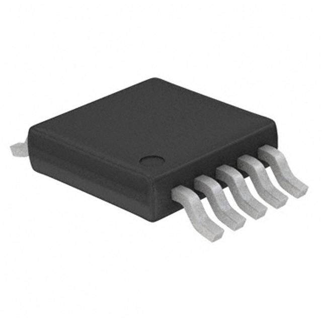
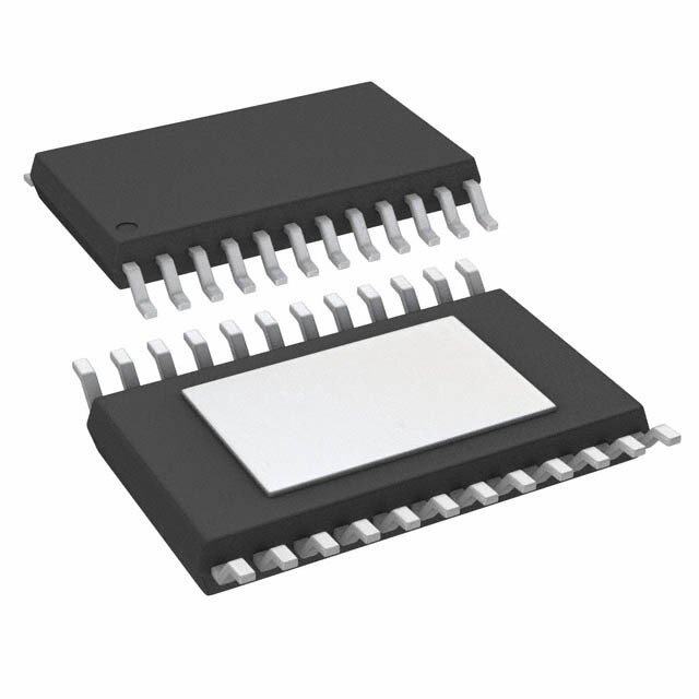
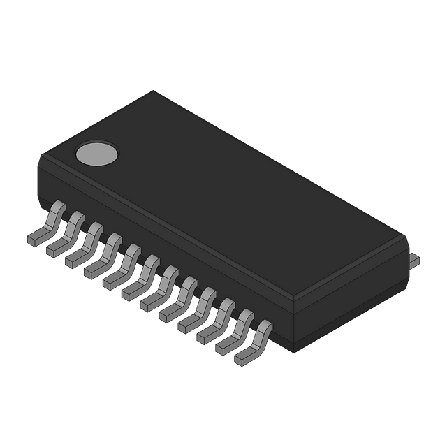
ICGOO电子元器件商城为您提供EL4340IUZ由Intersil设计生产,在icgoo商城现货销售,并且可以通过原厂、代理商等渠道进行代购。 EL4340IUZ价格参考。IntersilEL4340IUZ封装/规格:线性 - 放大器 - 视频放大器和频缓冲器, Video Amp, 3 2:1 Multiplexer-Amplifier 24-QSOP。您可以下载EL4340IUZ参考资料、Datasheet数据手册功能说明书,资料中有EL4340IUZ 详细功能的应用电路图电压和使用方法及教程。
| 参数 | 数值 |
| -3db带宽 | 500MHz |
| 产品目录 | 集成电路 (IC) |
| 描述 | IC MUX AMP TRPL 500MHZ 24-QSOP |
| 产品分类 | |
| 品牌 | Intersil |
| 数据手册 | |
| 产品图片 |
|
| 产品型号 | EL4340IUZ |
| rohs | 无铅 / 符合限制有害物质指令(RoHS)规范要求 |
| 产品系列 | - |
| 产品目录页面 | |
| 供应商器件封装 | 24-QSOP |
| 包装 | 管件 |
| 压摆率 | 870 V/µs |
| 安装类型 | 表面贴装 |
| 封装/外壳 | 24-SSOP(0.154",3.90mm 宽) |
| 应用 | 2:1 多路复用器-放大器 |
| 标准包装 | 55 |
| 电压-电源,单/双 (±) | - |
| 电流-电源 | 30mA |
| 电流-输出/通道 | 135mA |
| 电路数 | 3 |
| 输出类型 | - |






- 商务部:美国ITC正式对集成电路等产品启动337调查
- 曝三星4nm工艺存在良率问题 高通将骁龙8 Gen1或转产台积电
- 太阳诱电将投资9.5亿元在常州建新厂生产MLCC 预计2023年完工
- 英特尔发布欧洲新工厂建设计划 深化IDM 2.0 战略
- 台积电先进制程称霸业界 有大客户加持明年业绩稳了
- 达到5530亿美元!SIA预计今年全球半导体销售额将创下新高
- 英特尔拟将自动驾驶子公司Mobileye上市 估值或超500亿美元
- 三星加码芯片和SET,合并消费电子和移动部门,撤换高东真等 CEO
- 三星电子宣布重大人事变动 还合并消费电子和移动部门
- 海关总署:前11个月进口集成电路产品价值2.52万亿元 增长14.8%


PDF Datasheet 数据手册内容提取
DATASHEET EL4340, EL4342 FN7421 500MHz Triple Multiplexing Amplifiers Rev.4.00 Oct 4, 2017 The EL4340, EL4342 are fixed unity gain mux amps featuring Features high slew rates and excellent bandwidth for video switching. These devices feature a high impedance output state (HIZ) that • Triple 2:1 and 4:1 multiplexers for RGB enables the outputs of multiple devices to be wired together. A • Internally set gain-of-1 power-down mode (ENABLE) is included to turn off un-needed circuitry in power sensitive applications. The ENABLE pin, when • High speed three-state outputs (HIZ) pulled high, sets the EL4340, EL4342 into standby power • Power-down mode (ENABLE) mode - consuming just 18mW. An added feature in the EL4340 is a latch enable function (LE) that allows independent • Latch enable (EL4340) logic control using a common logic bus. • ±5V operation Ordering Information • ±870 V/µs slew rate • 500MHz bandwidth PART NUMBER PART PACKAGE PKG. • Typical supply currents 10mA/ch (EL4340) and 15.3mA/ch ( Notes1, 2, 3) MARKING (RoHS Compliant) DWG. # (EL4342) EL4340IUZ EL4340IUZ 24 Ld QSOP MDP0040 • Pb-free (RoHS compliant) EL4342ILZA 4342ILZ 32 Ld 5x6 QFN L32.5x6A Applications EL4340IUZ-EVAL Evaluation Board • HDTV/DTV analog inputs EL4342ILZA-EVAL Evaluation Board • Video projectors NOTES: 1. Add “-T13” suffix for 2.5k unit or “-T7” suffix for 1k unit tape and reel • Computer monitors options. Refer to TB347 for details on reel specifications. • Set-top boxes 2. These Intersil Pb-free plastic packaged products employ special Pb- free material sets, molding compounds/die attach materials, and • Security video 100% matte tin plate plus anneal (e3 termination finish, which is RoHS compliant and compatible with both SnPb and Pb-free • Broadcast video equipment soldering operations). Intersil Pb-free products are MSL classified TABLE 1. CHANNEL SELECT LOGIC TABLE EL4340 at Pb-free peak reflow temperatures that meet or exceed the Pb-free requirements of IPC/JEDEC J STD-020. S0 ENABLE HIZ LE OUTPUT 3. For Moisture Sensitivity Level (MSL), see product information page 0 0 0 0 INO (A, B, C) for EL4340, EL4342. For more information on MSL, refer to TB363. 1 0 0 0 IN1 (A, B, C) Related Literature X 1 X X Power-down • For a full list of related documents, visit our website X 0 1 X High Z - EL4340, EL4342 product pages X 0 0 1 Last S0 State Preserved TABLE 2. CHANNEL SELECT LOGIC TABLE EL4342 S1 S0 ENABLE HIZ OUTPUT 0 0 0 0 IN0 (A, B, C) 0 1 0 0 IN1 (A, B, C) 1 0 0 0 IN2 (A, B, C) 1 1 0 0 IN3 (A, B, C) X X 1 X Power-down X X 0 1 High Z FN7421 Rev.4.00 Page 1 of 14 Oct 4, 2017
EL4340, EL4342 Pin Configurations EL4340 EL4342 (24 LD QSOP) (32 LD QFN) TOP VIEW TOP VIEW A D A B C IN0A 1 24 NIC N 0 C 0 C 0 Z G N NI N NI N HI I I I 2 1 0 9 8 7 6 GND A 2 23 LE 3 3 3 2 2 2 2 IN1A 1 25ENABLE IN0B 3 22 ENABLE NIC 2 24NIC NIC 4 21 HIZ IN1B 3 23V+ GND B 5 20 OUTA AV=1 AV=1 NIC 4 22OUTA IN0C 6 19 V+ IN1C 5 21V- NIC 7 18 OUTB AV=1 GND B 6 THERMAL AV=1 20OUTB IN1A 8 17 OUTC PAD IN2A 7 19OUTC NIC 9 16 V- NIC 8 18S0 IN1B 10 AV=1 15 NIC AV=1 IN2B 9 17S1 GND C 11 14 S0 0 1 2 3 4 5 6 1 1 1 1 1 1 1 IN1C 12 13 NIC N2C D C N3A NIC N3B NIC N3C I N I I I G LATCHED ON HIGH LE THERMAL PAD INTERNALLY CONNECTED TO V-. NIC = NO INTERNAL CONNECTION PAD MUST BE TIED TO V- NIC = NO INTERNAL CONNECTION S0 EN0 EN0 DLQ S0 C IN0(A, B, C) OUT EN1 IN0(A, B, C) DECODE EN1 DLQ IN1(A, B, C) S1 DECODE IN1(A, B, C) OUT C EN2 IN2(A, B, C) IN3(A, B, C) AMPLIFIER BIAS EN3 LE HIZ AMPLIFIER BIAS ENABLE HIZ A LOGIC HIGH ON LE WILL LATCH THE LAST S0 STATE. THIS LOGIC STATE IS PRESERVED WHEN CYCLING HIZ ENABLE OR ENABLE FUNCTIONS. FIGURE 1. FUNCTIONAL DIAGRAM EL4340 FIGURE 2. FUNCTIONAL DIAGRAM EL4342 FN7421 Rev.4.00 Page 2 of 14 Oct 4, 2017
EL4340, EL4342 Pin Descriptions EL4342 EL4340 EQUIVALENT (32 Ld QFN) (24 Ld QSOP) PIN NAME CIRCUIT DESCRIPTION 1 8 IN1A Circuit 1 Channel 1 input for output amplifier “A” 2, 4, 8, 13, 15, 4, 7, 9, 13, 15, NIC Not Internally Connected; it is recommended these pins be tied to ground to minimize 24, 28, 30 24 crosstalk. 3 10 IN1B Circuit 1 Channel 1 input for output amplifier “B” 5 12 IN1C Circuit 1 Channel 1 input for output amplifier “C” 6 5 GNDB Circuit 4 Ground pin for output amplifier “B” 7 NA IN2A Circuit 1 Channel 2 input for output amplifier “A” 9 NA IN2B Circuit 1 Channel 2 input for output amplifier “B” 10 NA IN2C Circuit 1 Channel 2 input for output amplifier “C” 11 11 GNDC Circuit 4 Ground pin for output amplifier “C” 12 NA IN3A Circuit 1 Channel 3 input for output amplifier “A” 14 NA IN3B Circuit 1 Channel 3 input for output amplifier “B” 16 NA IN3C Circuit 1 Channel 3 input for output amplifier “C” 17 NA S1 Circuit 2 Channel selection pin MSB (binary logic code) 18 14 S0 Circuit 2 Channel selection pin. LSB (binary logic code) 19 17 OUTC Circuit 3 Output of amplifier “C” 20 18 OUTB Circuit 3 Output of amplifier “B” 21 16 V- Circuit 4 Negative power supply 22 20 OUTA Circuit 3 Output of amplifier “A” 23 19 V+ Circuit 4 Positive power supply 25 22 ENABLE Circuit 2 Device enable (active low). Internal pull-down resistor ensures the device will be active with no connection to this pin. A logic High on this pin puts device into power-down mode. In power-down mode only logic circuitry is active. All logic states are preserved post power-down. This state is not recommended for logic control where more than one MUX-amp share the same video output line. - 23 LE Circuit 2 Device latch enable on the EL4340. A logic high on LE will latch the last (S0, S1) logic state. HIZ and ENABLE functions are not latched with the LE pin. 26 21 HIZ Circuit 2 Output disable (active high). Internal pull-down resistor ensures the device will be active with no connection to this pin. A logic high, puts the outputs in a high impedance state. Use this state to control logic when more than one MUX-amp share the same video output line. 27 6 IN0C Circuit 1 Channel 0 for output amplifier “C” 29 3 IN0B Circuit 1 Channel 0 for output amplifier “B” 31 1 IN0A Circuit 1 Channel 0 for output amplifier “A” 32 2 GNDA Circuit 4 Ground pin for output amplifier “A” V+ V+ V+ IN LOGIC PIN 21k + 1.2V OUT - GND 33k V- V- V- CIRCUIT 1 CIRCUIT 2 CIRCUIT 3 V+ THERMAL HEAT SINK PAD ~1MΩ GNDA CAPACITIVELY V- GNDB COUPLED SUBSTRATE GNDC V- CIRCUIT 4 FN7421 Rev.4.00 Page 3 of 14 Oct 4, 2017
EL4340, EL4342 Absolute Maximum Ratings Thermal Information (TA = +25°C) Supply Voltage (V+ to V-) . . . . . . . . . . . . . . . . . . . . . . . . . . . . . . . . . . . . . . 11V Thermal Resistance (Typical) JA (°C/W) JC (°C/W) Input Voltage. . . . . . . . . . . . . . . . . . . . . . . . . . . . . . . . . . . . V- -0.5V, V+ +0.5V 32 Ld QFN Package (Notes4, 5) . . . . . . . . 35 1.3 to 8 Supply Turn-On Slew Rate . . . . . . . . . . . . . . . . . . . . . . . . . . . . . . . . . . 1V/µs 24 Ld QSOP Package (Note4) . . . . . . . . . . 88 N/A Digital & Analog Input Current (Note6). . . . . . . . . . . . . . . . . . . . . . . . 50mA Storage Temperature Range. . . . . . . . . . . . . . . . . . . . . . . .-65°C to +150°C Output Current (Continuous). . . . . . . . . . . . . . . . . . . . . . . . . . . . . . . . . 50mA Ambient Operating Temperature . . . . . . . . . . . . . . . . . . . . .-40°C to +85°C ESD Rating Operating Junction Temperature . . . . . . . . . . . . . . . . . . . .-40°C to +125°C Human Body Model (Per MIL-STD-883 Method 3015.7). . . . . . . . .2500V Power Dissipation. . . . . . . . . . . . . . . . . . . . . . . . . . . . . . . . . . . . . .See Curves Machine Model . . . . . . . . . . . . . . . . . . . . . . . . . . . . . . . . . . . . . . . . . . .300V Pb-free reflow profile . . . . . . . . . . . . . . . . . . . . . . . . . . . . . . . . . . . see TB493 CAUTION: Do not operate at or near the maximum ratings listed for extended periods of time. Exposure to such conditions may adversely impact product reliability and result in failures not covered by warranty. NOTES: 4. JA is measured in free air with the component mounted on a high-effective thermal conductivity test board with “direct attach” features. Refer to TB379. 5. For JC, the “case temp” location is the center of the exposed metal pad on the package underside. 6. If an input signal is applied before the supplies are powered up, the input current must be limited to these maximum values. IMPORTANT NOTE: All parameters having Min/Max specifications are guaranteed. Typical values are for information purposes only. Unless otherwise noted, all tests are at the specified temperature and are pulsed tests, therefore: TJ = TC = TA Electrical Specifications V+ = +5V, V- = -5V, GND = 0V, TA = +25°C, Input Video = 1VP-P and RL = 500Ω to GND, CL = 5pF unless otherwise specified. PARAMETER SYMBOL CONDITIONS MIN TYP MAX UNIT GENERAL Enabled Supply Current (EL4340) +IS Enabled No load, VIN = 0V, Enable Low 21.5 30 34 mA Enabled Supply Current (EL4342) 39 46 50 mA Enabled Supply Current (EL4340) -IS Enabled No load, VIN = 0V, Enable Low -32 -30 -21 mA Enabled Supply Current (EL4342) -48 -46 -36.5 mA Disabled Supply Current (EL4340) +IS Disabled No load, VIN = 0V, Enable High 1.75 2.8 4.2 mA Disabled Supply Current (EL4342) No load, VIN = 0V, Enable High 3 3.5 4 mA Disabled Supply Current -IS Disabled No load, VIN = 0V, Enable High 10 100 µA Positive and Negative Output Swing VOUT VIN = ±3.5V, RL = 500Ω ±3.1 ±3.4 V Output Current IOUT RL = 10Ω to GND ±80 ±135 mA Output Offset Voltage (EL4340) VOS -15 7 +15 mV Output Offset Voltage (EL4342) VOS -10 +10 mV Input Bias Current Ib VIN = 0V -0.5 -2 -3 µA HIZ Output Resistance ROUT HIZ = Logic High 1.4 MΩ Enabled Output Resistance ROUT HIZ = Logic Low 0.2 Ω Input Resistance RIN VIN = ±3.5V 10 MΩ Voltage Gain ACL or AV VIN = ±1.5V, RL= 500Ω 0.98 0.99 1.02 V/V Output Current in Three-State ITRI VOUT = 0V 8 15 22 µA LOGIC Input High Voltage (Logic Inputs) VIH 2 V Input Low Voltage (Logic Inputs) VIL 0.8 V Input High Current (Logic Inputs) IIH VH = 5V 215 270 340 µA Input Low Current (Logic Inputs) IIL VL = 0V 2 3 µA AC GENERAL 0.1% Settling Time tS Step = 1V 10 ns Power Supply Rejection Ratio PSRR (EL4340) DC, PSRR V+ and V- combined 52 72 dB Power Supply Rejection Ratio PSRR (EL4342) DC, PSRR V+ and V- combined 52 56 dB FN7421 Rev.4.00 Page 4 of 14 Oct 4, 2017
EL4340, EL4342 Electrical Specifications V+ = +5V, V- = -5V, GND = 0V, TA = +25°C, Input Video = 1VP-P and RL = 500Ω to GND, CL = 5pF unless otherwise specified. (Continued) PARAMETER SYMBOL CONDITIONS MIN TYP MAX UNIT Channel Isolation ISO f = 10MHz, Ch-Ch X-Talk and Off-Isolation, 75 dB CL= 1.5pF Differential Gain Error dG NTC-7, RL = 150, CL = 1.5pF 0.02 % Differential Phase Error dP NTC-7, RL = 150, CL = 1.5pF 0.02 ° -3dB Bandwidth BW CL = 1.5pF 500 MHz 0.1dB Bandwidth FBW CL = 1.5pF 60 MHz 0.1dB Bandwidth CL = 4.7pF 120 MHz Slew Rate SR 25% to 75%, RL = 150Ω, Input Enabled, ±870 V/µs CL=1.5pF SWITCHING CHARACTERISTICS Channel-to-Channel Switching Glitch VGLITCH VIN = 0V, CL = 1.5pF 40 mVP-P Enable Switching Glitch VIN = 0V CL = 1.5pF 300 mVP-P EL4340 HIZ Switching Glitch VIN = 0V CL = 1.5pF 200 mVP-P Channel-to-Channel Switching Glitch VGLITCH VIN = 0V CL = 1.5pF 20 mVP-P Enable Switching Glitch VIN = 0V CL = 1.5pF 200 mVP-P EL4342 HIZ Switching Glitch VIN = 0V CL = 1.5pF 200 mVP-P Channel Switching Time Low to High tSW-L-H 1.2V logic threshold to 10% movement of 18 ns analog output Channel Switching Time High to Low tSW-H-L 1.2V logic threshold to 10% movement of 20 ns analog output Rise and Fall Time tr, tf 10% to 90% 1.1 ns Propagation Delay tpd 10% to 10% 0.9 ns Latch Enable Hold time (EL4340 only) tLH LE = 0 10 ns Typical Performance Curves VS = ±5V, RL = 500Ω to GND, TA = +25°C, unless otherwise specified. 10 5 SOURCE POWER = -20dBm SOURCE POWER = -20dBm 8 CL = 16.5pF 4 IN (dB) 246 CL CC=LL 6==. 2 71p.13F.p5FpF N (dB) 123 GA AI D 0 G 0 E D Z -2 E -1 RMALI -4 CCLL == 42..72ppFF MALIZ -2 RLR =L =10 105Ω0Ω NO --86 CL INCLUDES 1.5pF CL = 1.5pF NOR --43 RL R=L 5 =0 01ΩkΩ BOARD CAPACITANCE -10 -5 1 10 100 1k 1 10 100 1k FREQUENCY (MHz) FREQUENCY (MHz) FIGURE 3. GAIN vs FREQUENCY vs CL FIGURE 4. GAIN vs FREQUENCY vs RL FN7421 Rev.4.00 Page 5 of 14 Oct 4, 2017
EL4340, EL4342 Typical Performance Curves VS = ±5V, RL = 500Ω to GND, TA = +25°C, unless otherwise specified. (Continued) 0.2 100 SOURCE POWER = -20dBm 0.1 CL = 4.7pF 0.0 ) ) B d-0.1 ( IN (-0.2 NCE 10 GA-0.3 CL = 1.5pF TA D IS ZE-0.4 ES ALI-0.5 T R 1 M U OR-0.6 TP N-0.7 OU -0.8 0.1 1 10 100 1k 0.1 1 10 100 1k FREQUENCY (MHz) FREQUENCY (MHz) FIGURE 5. 0.1dB GAIN vs FREQUENCY FIGURE 6. ROUT vs FREQUENCY 0.8 0.8 RL = 500Ω RL = 500Ω ) 0.6 CL = 1.5pF 0.6 CL = 1.5pF V ) ( V GE 0.4 E ( 0.4 A G T 0.2 A 0.2 L T O L V O UT 0 T V 0 P U T-0.2 P-0.2 U T O U -0.4 O-0.4 -0.6 -0.6 -0.8 -0.8 TIME (5ns/DIV) TIME (5ns/DIV) FIGURE 7. EL4340 TRANSIENT RESPONSE FIGURE 8. EL4342 TRANSIENT RESPONSE 0 0 -10 -10 INPUT X TO OUTPUT Y INPUT X TO OUTPUT Y -20 -20 CROSSTALK CROSSTALK -30 -30 (dB)--5400 OINFPFU ITS OXL TAOT IOOUNTPUT X (dB)--4500 OFF ISOLATION -60 -60 INPUT X TO OUTPUT X -70 -70 -80 -80 -90 -90 -100 -100 0.1 1 10 100 1k 0.1 1 10 100 1k FREQUENCY (MHz) FREQUENCY (MHz) FIGURE 9. EL4340 CROSSTALK AND OFF-ISOLATION FIGURE 10. EL4342 CROSSTALK AND OFF-ISOLATION FN7421 Rev.4.00 Page 6 of 14 Oct 4, 2017
EL4340, EL4342 Typical Performance Curves VS = ±5V, RL = 500Ω to GND, TA = +25°C, unless otherwise specified. (Continued) 20 20 10 PSRR (V+) 10 PSRR (V+) 0 0 -10 -10 -20 -20 B) B) RR (d--3400 PSRR (V-) RR (d--3400 PSRR (V-) S S P-50 P-50 -60 -60 -70 -70 -80 -80 0.3 1 10 100 1k 0.3 1 10 100 1k FREQUENCY (MHz) FREQUENCY (MHz) FIGURE 11. EL4340 PSRR CHANNELS A, B, C FIGURE 12. EL4342 PSRR CHANNELS A, B, C S0, S1 VIN = 0V S0, S1 VIN = 1V 50Ω 50Ω IV TERM. IV TERM. D D / / V V 1 1 0 0 V V V/DI 0 V/DI 20m VOUT A, B, C 0.5 0 VOUT A, B, C 20ns/DIV 20ns/DIV FIGURE 13. CHANNEL TO CHANNEL SWITCHING GLITCH VIN=0V FIGURE 14. CHANNEL TO CHANNEL TRANSIENT RESPONSE VIN=1V ENABLE VIN = 0V ENABLE VIN = 1V 50Ω 50Ω V TERM. V TERM. DI DI / / V V 1 1 V0 0 I D / mV VOUT A, B, C IV 0 D 100 V/ 0 VOUT A, B, C 1 20ns/DIV 20ns/DIV FIGURE 15. ENABLE SWITCHING GLITCH VIN = 0V FIGURE 16. ENABLE TRANSIENT RESPONSE VIN = 1V FN7421 Rev.4.00 Page 7 of 14 Oct 4, 2017
EL4340, EL4342 Typical Performance Curves VS = ±5V, RL = 500Ω to GND, TA = +25°C, unless otherwise specified. (Continued) HIZ VIN = 0V HIZ VIN = 1V 50Ω 50Ω DIV TERM. DIV TERM. / / V V 1 1 0 0 V I v/D 0 DIV VOUT A, B, C 0m VOUT A, B, C V/ 0 0 1 2 10ns/DIV 10ns/DIV FIGURE 17. HIZ SWITCHING GLITCH VIN = 0V FIGURE 18. HIZ TRANSIENT RESPONSE VIN = 1V JEDEC JESD51-7 HIGH EFFECTIVE THERMAL CONDUCTIVITY TEST BOARD-QFN EXPOSED DIEPAD SOLDERED TO PCB PER JESD51-5 60 3.0 ) Z H 2.857W / 50 W) 2.5 V E NOISE (n 4300 DISSIPATION ( 21..05 1.136W QFJNA3 =2 35°C/W LTAG 20 WER 1.0 O O QSOP24 V P 10 0.5 JA = 88°C/W 0 0 0 25 50 7585 100 125 150 100 1k 10k 100k FREQUENCY (Hz) AMBIENT TEMPERATURE (°C) FIGURE 19. INPUT NOISE vs FREQUENCY (OUTPUT A, B, C) FIGURE 20. PACKAGE POWER DISSIPATION vs AMBIENT TEMPERATURE JEDEC JESD51-3 LOW EFFECTIVE THERMAL CONDUCTIVITY TEST BOARD 1.2 W) 1.0 N ( 870mW O TI 0.8 A P QSOP24 SSI 0.6 758mW JA = 115°C/W DI R E 0.4 QFN32 OW JA = 125°C/W P 0.2 0 0 25 50 75 85 100 125 150 AMBIENT TEMPERATURE (°C) FIGURE 21. PACKAGE POWER DISSIPATION vs AMBIENT TEMPERATURE FN7421 Rev.4.00 Page 8 of 14 Oct 4, 2017
EL4340, EL4342 AC Test Circuits video cable-driving. The unity-gain current feedback output amplifiers are stable operating into capacitive loads and bandwidth is optimized with a load of 5pF in parallel with a EL4340, EL4342 500Ω. Total output capacitance can be split between the PCB VIN capacitance and an external load capacitor. 50Ω CL RL OR 5PF 500Ω Ground Connections 75Ω For the best isolation and crosstalk rejection, all GND pins and NIC pins must connect to the GND plane. FIGURE 22A. TEST CIRCUIT WITH OPTIMAL OUTPUT LOAD Control Signals S0, S1, ENABLE, LE, HIZ-These are binary coded, TTL/CMOS EL4340, EL4342 TEST compatible control inputs. The S0, S1 pins select the inputs. All RS EQUIPMENT VIN three amplifiers are switched simultaneously from their respective 475Ω inputs. The ENABLE, LE, HIZ pins are used to disable the part to 50Ω CL 50Ω 50Ω OR 5PF OR OR save power, latch in the last logic state and three-state the output 75Ω 75Ω 75Ω amplifiers, respectively. For control signal rise and fall times less than 10ns the use of termination resistors close to the part will minimize transients coupled to the output. FIGURE 22B. TEST CIRCUIT FOR MEASURING WITH 50Ω OR 75Ω INPUT TERMINATED EQUIPMENT Power-UP Considerations The ESD protection circuits use internal diodes from all pins the V+ and V- supplies. In addition, a dV/dT- triggered clamp is EL4340, EL4342 TEST connected between the V+ and V- pins, as shown in the RS EQUIPMENT Equivalent Circuits 1 through 4 section of the Pin Description VIN 50Ω OR 75Ω table. The dV/dT triggered clamp imposes a maximum supply 50Ω CL 50Ω turn-on slew rate of 1V/µs. Damaging currents can flow for power OR 5pF OR 75Ω 75Ω supply rates-of-rise in excess of 1V/µs, such as during hot plugging. Under these conditions, additional methods should be employed to ensure the rate of rise is not exceeded. FIGURE 22C. BACKLOADED TEST CIRCUIT FOR VIDEO CABLE APPLICATION. BANDWIDTH AND LINEARITY FOR RL Consideration must be given to the order in which power is LESS THAN 500Ω WILL BE DEGRADED. applied to the V+ and V- pins, as well as analog and logic input pins. Schottky diodes (Motorola MBR0550T or equivalent) FIGURE 22. TEST CIRCUITS connected from V+ to ground and V- to ground (Figure23) will shunt damaging currents away from the internal V+ and V- ESD Figure22A illustrates the optimum output load for testing AC diodes in the event that the V+ supply is applied to the device performance. Figure22B illustrates the optimun output load before the V- supply. when connecting to 50Ω input terminated equipment. If positive voltages are applied to the logic or analog video input Application Information pins before V+ is applied, current will flow through the internal ESD diodes to the V+ pin. The presence of large decoupling General capacitors and the loading effect of other circuits connected to V+, can result in damaging currents through the ESD diodes and The EL4340, EL4342 triple 2:1 and 4:1 MUX amps are ideal as other active circuits within the device. Therefore, adequate the matrix element of high performance switchers and routers. current limiting on the digital and analog inputs is needed to Key features include buffered high impedance analog inputs and prevent damage during the time the voltages on these inputs are excellent AC performance at output loads down to 150Ω for more positive than V+. V+ SUPPLY SCHOTTKY PROTECTION V+ V+ EXTERNAL LOGIC LOGIC CIRCUITS S0 CONTROL POWER GND GND V- V+ V+ SIGNAL IN0 V+ OUT V- DE-COUPLING IN1 V- CAPS V- V- V- SUPPLY FIGURE 23. SCHOTTKY PROTECTION CIRCUIT FN7421 Rev.4.00 Page 9 of 14 Oct 4, 2017
EL4340, EL4342 HIZ State frequency performance may be degraded for traces greater than one inch, unless strip line are used. An internal pull-down resistor ensures the device will be active with no connection to the HIZ pin. The HIZ state is established • Match channel-channel analog I/O trace lengths and layout within approximately 15ns (Figure18 on page8) by placing a symmetry. This will minimize propagation delay mismatches. logic high (>2V) on the HIZ pin. If the HIZ state is selected, the • Maximize use of AC de-coupled PCB layers. All signal I/O lines output is a high impedance 1.4MΩwithapproximately1.5pF in should be routed over continuous ground planes (for example, parallel with a 10µA bias current from the output. Use this state no split planes or PCB gaps under these lines). Avoid vias in the when more than one mux shares a common output. signal I/O lines. In the HIZ state the output is three-stated, and maintains its high • Use proper value and location of termination resistors. Z even in the presence of high slew rates. The supply current Termination resistors should be as close to the device as during this state is same as the active state. possible. ENABLE and Power-Down States • When testing use good quality connectors and cables, matching cable types and keeping cable lengths to a The enable pin is active low. An internal pull-down resistor minimum. ensures the device will be active with no connection to the ENABLE pin. The Power-down state is established within • Minimum of two power supply de-coupling capacitors are approximately 80ns (Figure16 on page7), if a logic high (>2V) is recommended (1000pF, 0.01µF) as close to the devices as placed on the ENABLE pin. In the Power-down state, the output possible - Avoid vias between the cap and the device because has no leakage but has a large variable capacitance (on the vias add unwanted inductance. Larger caps can be farther order of 15pF), and is capable of being back-driven. Under this away. When vias are required in a layout, they should be routed condition, large incoming slew rates can cause fault currents of as far away from the device as possible. tens of mA. Do not use this state as a high impedance output • The NIC pins are placed on both sides of the input pins. These when several MUX amps share the same output line. pins are not internally connected to the die. It is recommended these pins be tied to ground to minimize crosstalk. LE State The EL4340 is equipped with a Latch Enable pin. A logic high (>2V) The QFN Package Requires Additional PCB on the LE pin latches the last logic state. This logic state is Layout Rules for the Thermal Pad preserved when cycling HIZ or ENABLE functions. The thermal pad is electrically connected to V- supply through the Limiting the Output Current high resistance IC substrate. Its primary function is to provide heat sinking for the IC. However, because of the connection to No output short-circuit current limit exists on these parts. All the V- supply through the substrate, the thermal pad must be tied applications need to limit the output current to less than 50mA. to the V- supply to prevent unwanted current flow to the thermal Adequate thermal heat sinking of the parts is also required. pad. Do not tie this pin to GND as this could result in large back biased currents flowing between GND and V-. The EL4342 uses Application Example the package with pad dimensions of D2=2.48mm and Figure24 on page11 illustrates the use of the EL4342, two E2=3.4mm. ISL84517 SPST switches, and one NC7ST00P5X NAND gate to Maximum AC performance is achieved if the thermal pad is mux 3 different component video signals and one RGB video attached to a dedicated de-coupled layer in a multi-layered PC signal. The SPDT switches provide the sync signal for the RGB board. In cases where a dedicated layer is not possible, AC video and disconnects the sync signal for the component signal. performance may be reduced at upper frequencies. PC Board Layout The thermal pad requirements are proportional to power dissipation and ambient temperature. A dedicated layer The AC performance of this circuit depends greatly on the care eliminates the need for individual thermal pad area. When a taken in designing the PC board. The following are dedicated layer is not possible a 1” x 1” pad area is sufficient for recommendations to achieve optimum high frequency the EL4342 that is dissipating 0.5W in +50°C ambient. Pad area performance from your PC board. requirements should be evaluated on a case by case basis. • The use of low inductance components such as chip resistors and chip capacitors is strongly recommended. • Minimize signal trace lengths. Trace inductance and capacitance can easily limit circuit performance. Avoid sharp corners, use rounded corners when possible. Vias in the signal lines add inductance at high frequency and should be avoided. PCB traces greater than 1" begin to exhibit transmission line characteristics with signal rise/fall times of 1ns or less. High FN7421 Rev.4.00 Page 10 of 14 Oct 4, 2017
OcFN 5V 0.1µF 0.1µF -5V EL t 474 OPTIONAL SCHOTTKY PROTECTION 43 , 221 40 017Re YY12 311 INOA EL4342IL V+ 23 1nF 1nF , EL v IN1A 4 .4.00 YR3 172 IINN23AA OUTVA- 2221 342 OUTB 20 Pb1 29 OUTC 19 INOB Pb2 3 Pb3 9 IN1B GNDA 32 R16 R18 IN2B GNDB 6 500 500 G 14 IN3B GNDC 11 R17 NIC 2 500 Pr1 27 NIC 4 INOC Pr2 5 NIC 8 IN1C Pr3 10 NIC 13 IN2C B 16 NIC 15 IN3C NIC 24 NIC 28 R1 R3 R5 R7 R9 R11 NIC 30 75 75 75 75 75 75 HIZ 26 R2 R4 R6 R8 R10 R12 75 75 75 75 75 75 ENABLE 25 QFN S0 18 S1 17 5V 0.1µF 0.1µF -5V ISL84517IH-T H SYNC 1 V+5 1nF 1nF COM 3 V- 5V 0.1µF 0.1µF -5V SOT-23 2 NC IN 4 5V 0.1µF ISL84517IH-T V SYNC 1 V+ 5 1nF 1nF NC7ST00P5X COM 3 V- 5V 5 1nF P SOT-23 NC 2 1 a IN INPUT g 4 4 e 1 3 OGNUTD SC70INPUT 2 1 o f 1 LOGIC INPUTS 4 FIGURE 24. APPLICATION SHOWING THREE YPBPR CHANNELS AND ONE RGB+HV CHANNEL
EL4340, EL4342 Revision History The revision history provided is for informational purposes only and is believed to be accurate, but not warranted. Please visit our website to make sure you have the latest revision. DATE REVISION CHANGE Oct 4, 2017 FN7421.4 Applied new header/footer and formatting. Updated Related Literature section Moved Pin descriptions after Pin Configurations. Updated the following specifications in the EC table: +IS Enabled: changed min spec from 26mA to 21.5mA -IS Enabled: changed max spec from -24mA to -21mA +IS Disable Current: changed min spec from 2.3mA to 1.75mA and max spec from 3.3mA to 4.2mA Input Hi Current (IIH): changed max spec from 320µA to 340µA Input Bias Currents: changed min spec from -1µA to -0.5µA Added Revision History and About Intersil sections. About Intersil Intersil Corporation is a leading provider of innovative power management and precision analog solutions. The company's products address some of the largest markets within the industrial and infrastructure, mobile computing, and high-end consumer markets. For the most updated datasheet, application notes, related documentation, and related parts, see the respective product information page found at www.intersil.com. For a listing of definitions and abbreviations of common terms used in our documents, visit www.intersil.com/glossary. You can report errors or suggestions for improving this datasheet by visiting www.intersil.com/ask. Reliability reports are also available from our website at www.intersil.com/support. © Copyright Intersil Americas LLC 2005-2017. All Rights Reserved. All trademarks and registered trademarks are the property of their respective owners. For additional products, see www.intersil.com/en/products.html Intersil products are manufactured, assembled and tested utilizing ISO9001 quality systems as noted in the quality certifications found at www.intersil.com/en/support/qualandreliability.html Intersil products are sold by description only. Intersil may modify the circuit design and/or specifications of products at any time without notice, provided that such modification does not, in Intersil's sole judgment, affect the form, fit or function of the product. Accordingly, the reader is cautioned to verify that datasheets are current before placing orders. Information furnished by Intersil is believed to be accurate and reliable. However, no responsibility is assumed by Intersil or its subsidiaries for its use; nor for any infringements of patents or other rights of third parties which may result from its use. No license is granted by implication or otherwise under any patent or patent rights of Intersil or its subsidiaries. For information regarding Intersil Corporation and its products, see www.intersil.com FN7421 Rev.4.00 Page 12 of 14 Oct 4, 2017
EL4340, EL4342 Quad Flat No-Lead Plastic Package (QFN) L32.5x6A (One of 10 Packages in MDP0046) Micro Lead Frame Plastic Package (MLFP) 32 LEAD QUAD FLAT NO-LEAD PLASTIC PACKAGE (COMPLIANT TO JEDEC MO-220) A MILLIMETERS D SYMBOL MIN NOMINAL MAX NOTES 1)2) B NN-N- A 0.80 0.90 1.00 - (( A1 0.00 0.02 0.05 - 1 D 5.00 BSC - 2 PIN #1 3 I.D. MARK D2 2.48 REF - E E 6.00 BSC - E2 3.40 REF - L 0.45 0.50 0.55 - b 0.17 0.22 0.27 - 2X 0.075C (N c 0.20 REF - /2) 2X e 0.50 BSC - 0.075C N 32 REF 4 TOP VIEW ND 7 REF 6 S NE 9 REF 5 D EA 0.10 M CAB Rev 1 2/09 L N b NOTES: L (N-2)(N-1)N PIN #1 I.D. 1. Dimensioning and tolerancing per ASME Y14.5M-1994. 3 2. Tiebar view shown is a non-functional feature. 1 3. Bottom-side pin #1 I.D. is a diepad chamfer as shown. 2 3 4. N is the total number of terminals on the device. 5. NE is the number of terminals on the “E” side of the package (E2) (orY-direction). 6. ND is the number of terminals on the “D” side of the package (orX-direction). ND = (N/2)-NE. NE 5 7. Inward end of terminal may be square or circular in shape with radius (b/2) as shown. 2) N/ ( 7 (D2) BOTTOM VIEW 0.10 C e C (c) 2 SEATING A C PLANE 0.08 C SEE DETAIL "X" (L) N LEADS A1 & EXPOSED PAD N LEADS SIDE VIEW DETAIL X For the most recent package outline drawing, see L32.5x6A. FN7421 Rev.4.00 Page 13 of 14 Oct 4, 2017
EL4340, EL4342 Quarter Size Outline Plastic Packages MDP0040 Family (QSOP) QUARTER SIZE OUTLINE PLASTIC PACKAGES FAMILY A INCHES D SYMBOL QSOP16 QSOP24 QSOP28 TOLERANCE NOTES N (N/2)+1 A 0.068 0.068 0.068 Max. - A1 0.006 0.006 0.006 ±0.002 - PIN #1 A2 0.056 0.056 0.056 ±0.004 - I.D. MARK E E1 b 0.010 0.010 0.010 ±0.002 - c 0.008 0.008 0.008 ±0.001 - D 0.193 0.341 0.390 ±0.004 1, 3 1 (N/2) E 0.236 0.236 0.236 ±0.008 - B 0.010 CAB E1 0.154 0.154 0.154 ±0.004 2, 3 e 0.025 0.025 0.025 Basic - e H L 0.025 0.025 0.025 ±0.009 - C L1 0.041 0.041 0.041 Basic - SEATING N 16 24 28 Reference - PLANE 0.004 C 0.007 CAB b Rev. F 2/07 NOTES: 1. Plastic or metal protrusions of 0.006” maximum per side are not included. L1 2. Plastic interlead protrusions of 0.010” maximum per side are not included. A 3. Dimensions “D” and “E1” are measured at Datum Plane “H”. c 4. Dimensioning and tolerancing per ASME Y14.5M-1994. SEE DETAIL "X" 0.010 A2 GAUGE PLANE L A1 4°±4° DETAIL X For the most recent package outline drawing, see MDP0040. FN7421 Rev.4.00 Page 14 of 14 Oct 4, 2017
 Datasheet下载

