ICGOO在线商城 > E-L6925D013TR
- 型号: E-L6925D013TR
- 制造商: STMicroelectronics
- 库位|库存: xxxx|xxxx
- 要求:
| 数量阶梯 | 香港交货 | 国内含税 |
| +xxxx | $xxxx | ¥xxxx |
查看当月历史价格
查看今年历史价格
E-L6925D013TR产品简介:
ICGOO电子元器件商城为您提供E-L6925D013TR由STMicroelectronics设计生产,在icgoo商城现货销售,并且可以通过原厂、代理商等渠道进行代购。 提供E-L6925D013TR价格参考以及STMicroelectronicsE-L6925D013TR封装/规格参数等产品信息。 你可以下载E-L6925D013TR参考资料、Datasheet数据手册功能说明书, 资料中有E-L6925D013TR详细功能的应用电路图电压和使用方法及教程。
| 参数 | 数值 |
| 产品目录 | 集成电路 (IC) |
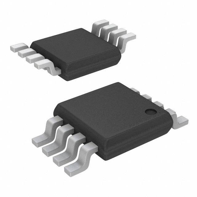
| 描述 | IC REG BUCK SYNC ADJ 0.8A 8MSOP |
| 产品分类 | |
| 品牌 | STMicroelectronics |
| 数据手册 | |
| 产品图片 |
|
| 产品型号 | E-L6925D013TR |
| PWM类型 | 电流模式 |
| rohs | 无铅 / 符合限制有害物质指令(RoHS)规范要求 |
| 产品系列 | - |
| 产品目录页面 | |
| 供应商器件封装 | 8-MSOP |
| 其它名称 | 497-4594-1 |
| 包装 | 剪切带 (CT) |
| 同步整流器 | 是 |
| 安装类型 | 表面贴装 |
| 封装/外壳 | 8-TSSOP,8-MSOP(0.118",3.00mm 宽) |
| 工作温度 | -40°C ~ 150°C |
| 标准包装 | 1 |
| 电压-输入 | 2.7 V ~ 5.5 V |
| 电压-输出 | 0.6 V ~ 5.5 V |
| 电流-输出 | 800mA |
| 类型 | 降压(降压) |
| 输出数 | 1 |
| 输出类型 | 可调式 |
| 频率-开关 | 600kHz |





- 商务部:美国ITC正式对集成电路等产品启动337调查
- 曝三星4nm工艺存在良率问题 高通将骁龙8 Gen1或转产台积电
- 太阳诱电将投资9.5亿元在常州建新厂生产MLCC 预计2023年完工
- 英特尔发布欧洲新工厂建设计划 深化IDM 2.0 战略
- 台积电先进制程称霸业界 有大客户加持明年业绩稳了
- 达到5530亿美元!SIA预计今年全球半导体销售额将创下新高
- 英特尔拟将自动驾驶子公司Mobileye上市 估值或超500亿美元
- 三星加码芯片和SET,合并消费电子和移动部门,撤换高东真等 CEO
- 三星电子宣布重大人事变动 还合并消费电子和移动部门
- 海关总署:前11个月进口集成电路产品价值2.52万亿元 增长14.8%
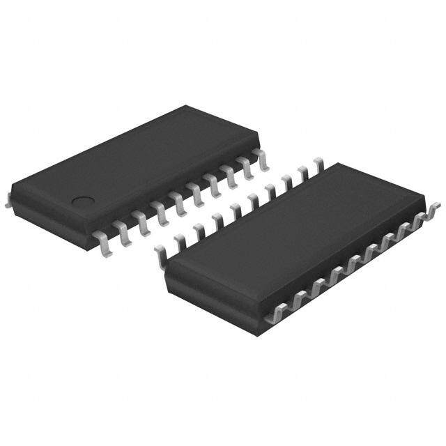




PDF Datasheet 数据手册内容提取
L6925D HIGH EFFICIENCY MONOLITHIC SYNCHRONOUS STEP DOWN REGULATOR 1 FEATURES Figure 1. Package ■ 2.7V TO 5.5V BATTERY INPUT RANGE ■ HIGH EFFICIENCY: UP TO 95% ■ INTERNAL SYNCHRONOUS SWITCH ■ NO EXTERNAL SCHOTTKY REQUIRED MSOP8 ■ EXTREMELY LOW QUIESCENT CURRENT Table 1. Order Codes ■ 800mA MAX OUTPUT CURRENT ■ ADJUSTABLE OUTPUT VOLTAGE FROM 0.6V Part Number Package ■ LOW DROP-OUT OPERATION: UP TO100% L6925D MSOP8 (Tube) DUTY CYCLE L6925D013TR Tape & Reel ■ SELECTABLE LOW NOISE/LOW CONSUMPTION MODE AT LIGHT LOAD 2 DESCRIPTION ■ LOW BATTERY INPUT The device is dc-dc monolithic regulator specifically ■ LOW BATTERY OUTPUT designed to provide extremely high efficiency. ■ ±1% OUTPUT VOLTAGE ACCURACY The device has on UVLO set at 2.7V cause it is part- ■ CURRENT-MODE CONTROL icurarly thought for single Li-ion cell applications. ■ 600kHz SWITCHING FREQUENCY Output voltage can be selected by an external divider down to 0.6V. Duty Cycle can saturate to 100% al- ■ EXTERNALLY SYNCHRONIZABLE FROM lowing low drop-out operation. 500kHz TO 1.4MHz ■ OVP The device is based on a 600kHz fixed-frequency, current mode-architecture. Low Consumption Mode ■ SHORT CIRCUIT PROTECTION operation can be selected at light load conditions, al- lowing switching losses to be reduced. L6925D is ex- 1.1 APPLICATIONS ternally synchronizable with a clock which makes it ■ BATTERY-POWERED EQUIPMENTS useful in noise-sensitive applications. ■ PORTABLE INSTRUMENTS LBI pin can be used to have a LBO signal when the ■ CELLULAR PHONES Battery voltage is lower than a preset value. Other features like, Overvoltage protection, Shortcircuit ■ PDAs AND HAND HELD TERMINALS protection and Thermal Shutdown (150°C) are also ■ DSC present. ■ GPS Figure 2. Application Test Circuit V =2.7V to 5.5V SYNC IN 7 L 6.8µH V =1.8V OUT V 5 C1 R2 CC 6 LX 10µF 600K R4 C4 6.3V LBI 1 200K 10µF 6.3V VFB R1 3 100K LBO 8 2 4 R3 COMP GND 100K C2 220pF D01IN1238B Rev. 3 September 2004 1/6
L6925D Table 2. Absolute Maximum Ratings Symbol Parameter Value Unit V6 Input voltage -0.3 to 6 V V5 Output switching voltage -1 to VCC V V1, V8 Low Battery Input, Low Battery Output -0.3 to VCC V V3 Feedback voltage -0.3 to VCC V V2 Error Amplifier Output Voltage -0.3 to VCC V V7 Syncronization / Mode Selector -0.3 to VCC V Ptot Power dissipation at Tamb=70°C 0.45 W Tj Junction operating temperature range -40 to 150 °C Tstg Storage temperature range -65 to 150 °C LX Pin Maximum Withstanding Voltage Range Test Condition: CDF- ±1000 V AEC-Q100-002- “Human Body Model” Acceptance Criteria: Other pins ±2000 V “Normal Performance’ Figure 3. Pin Connection LBI 1 8 LBO COMP 2 7 SYNC VFB 3 6 V CC GND 4 5 LX D01IN1239A/mod Table 3. Thermal Data Symbol Parameter Value Unit Rth j-amb Thermal Resistance Junction to Ambient 180 °C/W Table 4. Pin Functions N Name Description 1 LBI Battery low voltage detector input. The internal threshold is set to 0.6V. The external threshold can be adjusted by using an external resistor divider. 2 COMP Error amplifier output. Compensate it with a 220pF capacitor 3 VFB Error amplifier input. The output voltage can be adjusted by using an external resistor divider connected to this pin (VFB = 0.6V). 4 GND Ground. 5 LX Switch node connection to the inductor. 6 VCC Input voltage. 7 SYNC This pin allows to select Low Noise/ Low Consumption Mode or to sychronize the device. 8 LBO Battery low voltage detector output. If the voltage at the LBI pin drops below the internal thrshold, LBO goes low. The LBO is an open drain output. A pull_up resistor should be connected between the pin and the output voltage 2/6
L6925D Table 5. ELECTRICAL CHARACTERISTICS (TJ = 25°C, VCC = 3.6V unless otherwise specified) Symbol Parameter Test Condition Min Typ Max Unit Vcc Operating input voltage After Turn On 2.7 5.5 V Vcc ON Turn On threshold 2.8 V Vcc OFF Turn Off threshold 2.65 V Vcc hys Hysteresis 150 mV Rp High side Ron Vcc = 3.6V, Ilx =100mA 240 mΩ Rn Low side Ron Vcc = 3.6V, Ilx =100mA 215 mΩ Ilim Peak current limit Vcc = 3.6V 1.2 A Valley current limit Vcc = 3.6V 1.4 A Vout Output voltage range 0.6 Vcc V fosc Oscillator frequency 600 KHz fsync Sync mode clock (*) 500 1400 KHz DC CHARACTERISTICS Iq Quiescent current Vsync = 0V, no load, 230 µA (low noise mode) VFB > 0.6V Quiescent current Vsync = Vcc, no load, 25 µA (low cunsumption mode) VFB > 0.6V Ish Shutdown current Vcc < 2.7V, VFB > 0.6V 0.2 µA Ilx LX leakage current (*) Vcc < 2.7V, VLX = Vcc 1 µA Vcc < 2.7V, VLX = 0V 1 µA ERROR AMPLIFIER CHARACTERISTICS Vfb Voltage feedback 0.593 0.6 0.607 V Ifb Feedback input current (*) VFB = 0.6V 25 nA SYNC/MODE FUNCTION Vsync_H Sync mode threshold high 1.3 V Vsync_L Sync mode threshold low 0.5 V LB SECTION VLBI LBI Threshold 0.6 V VLBO LBO Logic Low Isink = 1mA, Vcc = 3.6V, 0.2 0.4 V VLBI < 0.6V ILK-LBO LBO Leakage Current (*) V LBO = 3.6V, Vcc = 3.6V, 50 nA VLBI > 0.6V PROTECTIONS HOVP Hard overvoltage threshold 10 %Vout (*) Guaranteed by design 3/6
L6925D Figure 4. MSOP8 Mechanical Data & Package Dimensions mm inch DIM. OUTLINE AND MIN. TYP. MAX. MIN. TYP. MAX. MECHANICAL DATA A 1.10 0.043 A1 0.050 0.150 0.002 0.006 A2 0.750 0.850 0.950 0.03 0.033 0.037 b 0.250 0.400 0.010 0.016 c 0.130 0.230 0.005 0.009 D (1) 2.900 3.000 3.100 0.114 0.118 0.122 E 4.650 4.900 5.150 0.183 0.193 0.20 E1 (1) 2.900 3.000 3.100 0.114 0.118 0.122 e 0.650 0.026 L 0.400 0.550 0.700 0.016 0.022 0.028 L1 0.950 0.037 k 0˚ (min.) 6˚ (max.) aaa 0.100 0.004 MSOP8 Note: 1. D and F does not include mold flash or protrusions. (Body 3mm) Mold flash or potrusions shall not exceed 0.15mm (.006inch) per side. 4/6
L6925D Table 6. Revision History Date Revision Description of Changes January 2004 2 First Issue in EDOCS DMS September 2004 3 Changed Style-sheet and Table 2 5/6
L6925D Information furnished is believed to be accurate and reliable. However, STMicroelectronics assumes no responsibility for the consequences of use of such information nor for any infringement of patents or other rights of third parties which may result from its use. No license is granted by implication or otherwise under any patent or patent rights of STMicroelectronics. Specifications mentioned in this publication are subject to change without notice. This publication supersedes and replaces all information previously supplied. STMicroelectronics products are not authorized for use as critical components in life support devices or systems without express written approval of STMicroelectronics. The ST logo is a registered trademark of STMicroelectronics. All other names are the property of their respective owners © 2004 STMicroelectronics - All rights reserved STMicroelectronics group of companies Australia - Belgium - Brazil - Canada - China - Czech Republic - Finland - France - Germany - Hong Kong - India - Israel - Italy - Japan - Malaysia - Malta - Morocco - Singapore - Spain - Sweden - Switzerland - United Kingdom - United States of America www.st.com 6/6
 Datasheet下载
