ICGOO在线商城 > DZ3X062D0L

 Datasheet下载
- 型号: DZ3X062D0L
- 制造商: Panasonic Corporation
- 库位|库存: xxxx|xxxx
- 要求:
| 数量阶梯 | 香港交货 | 国内含税 |
| +xxxx | $xxxx | ¥xxxx |
查看当月历史价格
查看今年历史价格
DZ3X062D0L产品简介:
ICGOO电子元器件商城为您提供DZ3X062D0L由Panasonic Corporation设计生产,在icgoo商城现货销售,并且可以通过原厂、代理商等渠道进行代购。 提供DZ3X062D0L价格参考以及Panasonic CorporationDZ3X062D0L封装/规格参数等产品信息。 你可以下载DZ3X062D0L参考资料、Datasheet数据手册功能说明书, 资料中有DZ3X062D0L详细功能的应用电路图电压和使用方法及教程。
| 参数 | 数值 |
| 产品目录 | |
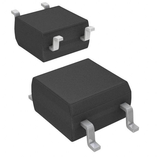
| 描述 | DIODE ZENER DUAL 6.2V MINI3稳压二极管 6.2V 5% 200mW GL WNG 2.9x2.8mm |
| 产品分类 | 二极管/齐纳阵列分离式半导体 |
| 品牌 | Panasonic Electronic Components - Semiconductor ProductsPanasonic |
| 产品手册 | |
| 产品图片 |
|
| rohs | 符合RoHS无铅 / 符合限制有害物质指令(RoHS)规范要求 |
| 产品系列 | 二极管与整流器,稳压二极管,Panasonic DZ3X062D0L- |
| 数据手册 | http://industrial.panasonic.com/www-cgi/jvcr13pz.cgi?E+SC+4+AND7004+DZ3X062D+8+WW |
| 产品型号 | DZ3X062D0LDZ3X062D0L |
| 不同If时的电压-正向(Vf) | 1V @ 10mA |
| 不同 Vr时的电流-反向漏电流 | 200nA @ 4V |
| 产品 | Zener Diode |
| 产品培训模块 | http://www.digikey.cn/PTM/IndividualPTM.page?site=cn&lang=zhs&ptm=26113 |
| 产品种类 | |
| 供应商器件封装 | 迷你型3-G3-B |
| 其它名称 | DZ3X062D0LDKR |
| 功率-最大值 | 200mW |
| 功率耗散 | 200 mW |
| 包装 | Digi-Reel® |
| 商标 | Panasonic |
| 安装类型 | 表面贴装 |
| 安装风格 | SMD/SMT |
| 容差 | - |
| 封装 | Reel |
| 封装/外壳 | TO-236-3,SC-59,SOT-23-3 |
| 封装/箱体 | Mini3-G3-B |
| 工作温度 | - |
| 工厂包装数量 | 3000 |
| 最大反向漏泄电流 | 200 nA |
| 最大工作温度 | + 85 C |
| 最大齐纳阻抗 | 50 Ohms |
| 最小工作温度 | - 40 C |
| 标准包装 | 1 |
| 正向电压下降 | 1 V at 10 mA |
| 电压-齐纳(标称值)(Vz) | 6.2V |
| 电压容差 | 5 % |
| 电压温度系数 | 2.3 mV/C |
| 配置 | 1 对共阳极Dual Common Anode |
| 阻抗(最大值)(Zzt) | 50 欧姆 |
| 齐纳电压 | 6.2 V |


- 商务部:美国ITC正式对集成电路等产品启动337调查
- 曝三星4nm工艺存在良率问题 高通将骁龙8 Gen1或转产台积电
- 太阳诱电将投资9.5亿元在常州建新厂生产MLCC 预计2023年完工
- 英特尔发布欧洲新工厂建设计划 深化IDM 2.0 战略
- 台积电先进制程称霸业界 有大客户加持明年业绩稳了
- 达到5530亿美元!SIA预计今年全球半导体销售额将创下新高
- 英特尔拟将自动驾驶子公司Mobileye上市 估值或超500亿美元
- 三星加码芯片和SET,合并消费电子和移动部门,撤换高东真等 CEO
- 三星电子宣布重大人事变动 还合并消费电子和移动部门
- 海关总署:前11个月进口集成电路产品价值2.52万亿元 增长14.8%


PDF Datasheet 数据手册内容提取
Doc No. TT4-EA-12584 Revision. 4 Product Standards Zener Diode DZ3X062D0L DZ3X062D0L Silicon epitaxial planar type Unit: mm 2.9 For surge absorption circuit 0.4 0.16 3 Features Excellent rising characteristics of zener current Iz Low zener operating resistance Rz .5.8 12 Halogen-free / RoHS compliant (EU RoHS / UL-94 V-0 / MSL:Level 1 compliant) 1 2 1.1 Marking Symbol:01 (0.95)(0.95) 1.9 Packaging 1. Cathode1 Embossed type (Thermo-compression sealing) 3 000 pcs / reel (standard) 2. Cathode2 3. Anode1,2 Absolute Maximum Ratings Ta = 25 C Panasonic Mini3-G3-B Parameter Symbol Rating Unit JEITA SC-59A Total power dissipation *1 PT 200 mW Code TO-236AA/SOT-23 Electrostatic discharge *2 ESD ±10 kV Junction temperature Tj 150 °C Operating ambient temperature Topr -40 to +85 °C Internal Connection Storage temperature Tstg -55 to +150 °C Note) *1: Mounted on glass epoxy print board. ( 45 mm x 45 mm x 1 mm) 3 (2 Diode total) Solder in ( 1.0 mm x 1.0 mm) *2: Test method:IEC61000_4_2(C = 150 pF,R = 330 , Contact discharge:10 times) 1 2 Electrical Characteristics Ta = 25 C 3 C Parameter Symbol Conditions Min Typ Max Unit Forward voltage VF IF = 10 mA 1.0 V Zener voltage *1, *2 VZ IZ = 5 mA 5.89 6.51 V Zener operating resistance RZ IZ = 5 mA 50 Zener rise operating resistance RZK IZ = 0.5 mA 100 Reverse current IR VR = 4 V 0.2 μA Temperature coefficient of zener voltage *3 SZ IZ = 5 mA 2.3 mV/°C Note) 1. Measuring methods are based on JAPANESE INDUSTRIAL STANDARD JIS C 7031 Measuring methods for Diodes. 2. *1: The temperature must be controlled 25°C for VZ mesurement. VZ value measured at other temperature must be adjusted to VZ (25°C) *2: VZ guaranted 20 ms after current flow. *3: Tj = 25°C to 150°C Page 1 of 4 Established :2010-05-17 Revised :2013-10-22
Doc No. TT4-EA-12584 Revision. 4 Product Standards Zener Diode DZ3X062D0L Technical Data ( reference ) PT - Ta IF - VF 250 1.E+00 W) Mounted on glass epoxy print board (2 diode total) Ta = 25 ℃ m Board size : 45 mm × 45 mm x 1 mm 1.E-01 T ( 200 Solder in : 1.0 mm x 1.0 mm A) ation P 150 ent IF ( 1.E-02 er dissip 100 ard curr 11..EE--0043 w w al po 50 For 1.E-05 ot T 0 1.E-06 0 20 40 60 80 100 120 140 160 180 200 0.0 0.2 0.4 0.6 0.8 1.0 1.2 Ambient temperature Ta (°C) Forward voltage VF (V) IZ - VZ IR - VR 1.E-01 1.E-06 Ta = 25 ℃ 1.E-07 1.E-02 nt IZ (A)1.E-03 25 ℃ Ta = 125 ℃ ent IR (A)1.E-08 urre -40 ℃ 85 ℃ curr1.E-09 ner c1.E-04 erse 1.E-10 e v Z e 1.E-05 R 1.E-11 1.E-06 1.E-12 0 2 4 6 8 10 12 0 1 2 3 4 Zener voltage VZ (V) Reverse voltage VR (V) RZ - IZ SZ - IZ 100 5 Ta = 25 ℃ er n ) ze 3 ance RZ 10 cient of mV/°C) 1 ner operating resist 1 parature coeffivoltage SZ ( --31 e m Z e T 0.1 -5 0.0001 0.001 0.01 0.1 0 2 4 6 8 10 Zener current IZ (A) Zener current IZ (mA) Page 2 of 4 Established :2010-05-17 Revised :2013-10-22
Doc No. TT4-EA-12584 Revision. 4 Product Standards Zener Diode DZ3X062D0L Technical Data ( reference ) Rth- t Ct - VR 40 1000 F) 35 Ta = 25 ℃ e Ct (p 30 f = 1 MHz h (°C/W) 100 Rth(j-l) = 100 ℃/W (1) (2) nc 25 Rt cita 20 nce a a p st ca 15 esi nal 10 mal r 10 (1) Non-heat sink mi er (2) Mounted on glass epoxy print board. Ter 5 Th Board size : 45 mm × 45 mm x 1 mm Solder in : 1.0 mm x 1.0 mm 0 1 0 1 2 3 4 5 0.001 0.01 0.1 1 10 100 1000 Reverse voltage VR (V) Time t (s) PZSM - tw 100 Ta = 25 ℃ geW) surM ( e S sZ 10 evern P etitive rssipatio 1 Non-reppower di 0.1 100 1000 10000 Pulse width tw (μs) Page 3 of 4 Established :2010-05-17 Revised :2013-10-22
Doc No. TT4-EA-12584 Revision. 4 Product Standards Zener Diode DZ3X062D0L Mini3-G3-B Unit: mm +0.20 2.90-0.05 +0.10 +0.10 0.16-0.06 0.40-0.05 3 55 20 23 .. .. 00 00 +- +- 0 8 5 . . 2 1 ) ° 5 1 2 ( ) 2 5 . (0.95) (0.95) 6 0 . ± 0 4 1.9±0.1 ( 0. (10°) +0.21-0.1 +0.31-0.1 . . 1 1 1 . 0 o t 0 Land Pattern (Reference) (Unit: mm) 1.0 0 . 1 4 . 2 1.9 Page 4 of 4 Established :2010-05-17 Revised :2013-10-22
Request for your special attention and precautions in using the technical information and semiconductors described in this book (1) If anyof theproductsor technicalinformationdescribedinthisbook is tobe exported or provided to non-residents, the lawsandregulationsoftheexportingcountry,especially,thosewithregardtosecurityexportcontrol,mustbeobserved. (2)Thetechnicalinformationdescribedinthisbookisintendedonlytoshowthemaincharacteristicsandapplicationcircuit examples of the products. No license is granted in and to any intellectual property right or other right owned by Panasonic Corporation or any other company. Therefore, no responsibility is assumed by our company as to the infringement upon any such right owned by any other company which may arise as a result of the use of technical informationde-scribedinthisbook. (3) The products described in this book are intended to be used for general applications (such as office equipment, communicationsequipment,measuringinstrumentsandhouseholdappliances),orforspecificapplicationsasexpressly statedinthisbook. Please consult with our sales staff in advance for information on the following applications, moreover please exchange documentsseparatelyontermsofuseetc.:Specialapplications(suchasforin-vehicleequipment,airplanes,aerospace, automotive equipment, traffic signaling equipment, combustion equipment, medical equipment and safety devices) in which exceptional quality and reliability are required, or if the failure or malfunction of the products may directly jeopardizelifeorharmthehumanbody. Unlessexchangingdocumentsontermsofuseetc.inadvance,itistobeunderstoodthatourcompanyshallnotbeheld responsiblefor anydamageincurred asaresult of or inconnection with your usingthe productsdescribed inthisbook foranyspecialapplication. (4) The products and product specifications described in this book are subject to change without notice for modification and/orimprovement.Atthefinalstageofyourdesign,purchasing,oruseoftheproducts,therefore,askforthemostup- to-dateProductStandardsinadvancetomakesurethatthelatestspecificationssatisfyyourrequirements. (5) When designing your equipment, comply with the range of absolute maximum rating and the guaranteed operating conditions(operatingpowersupplyvoltageandoperatingenvironmentetc.).Especially,pleasebecarefulnottoexceed the range of absolute maximum rating on the transient state, such as power-on, power-off and mode-switching. Other- wise,wewillnotbeliableforanydefectwhichmayariselaterinyourequipment. Even when the products are used within the guaranteed values, take into the consideration of incidence of break down and failure mode, possible to occur to semiconductor products. Measures on the systems such as redundant design, arrestingthespreadoffireorpreventingglitcharerecommendedinordertopreventphysicalinjury,fire,socialdamages, forexample,byusingtheproducts. (6) Comply with the instructions for use in order to prevent breakdown and characteristics change due to external factors (ESD, EOS, thermal stress and mechanical stress) at the time of handling, mounting or at customer's process. We do notguaranteequalityfordisassembledproductsortheproductre-mountedafterremovingfromthemountingboard. Whenusingproductsforwhichdamp-proofpackingisrequired,satisfytheconditions,suchasshelflifeandtheelapsed timesincefirstopeningthepackages. (7) When reselling products described in this book to other companies without our permission and receiving any claim of requestfromtheresaledestination,pleaseunderstandthatcustomerswillbeartheburden. (8) This book may be not reprinted or reproduced whether wholly or partially, without the prior written permission of our company. No.010618