ICGOO在线商城 > 集成电路(IC) > 接口 - 串行器,解串行器 > DS92LV3221TVS/NOPB

 Datasheet下载
- 型号: DS92LV3221TVS/NOPB
- 制造商: Texas Instruments
- 库位|库存: xxxx|xxxx
- 要求:
| 数量阶梯 | 香港交货 | 国内含税 |
| +xxxx | $xxxx | ¥xxxx |
查看当月历史价格
查看今年历史价格
DS92LV3221TVS/NOPB产品简介:
ICGOO电子元器件商城为您提供DS92LV3221TVS/NOPB由Texas Instruments设计生产,在icgoo商城现货销售,并且可以通过原厂、代理商等渠道进行代购。 DS92LV3221TVS/NOPB价格参考。Texas InstrumentsDS92LV3221TVS/NOPB封装/规格:接口 - 串行器,解串行器, 1.6Gbps Serializer 32 Input 2 Output 64-TQFP (10x10)。您可以下载DS92LV3221TVS/NOPB参考资料、Datasheet数据手册功能说明书,资料中有DS92LV3221TVS/NOPB 详细功能的应用电路图电压和使用方法及教程。
| 参数 | 数值 |
| 产品目录 | 集成电路 (IC)半导体 |
| 描述 | IC SERIALIZER LVDS 32BIT 64TQFP串行器/解串器 - Serdes 20-50MHz 32B CH Link II Serializer |
| 产品分类 | |
| 品牌 | Texas Instruments |
| 产品手册 | |
| 产品图片 |
|
| rohs | 符合RoHS无铅 / 符合限制有害物质指令(RoHS)规范要求 |
| 产品系列 | 接口 IC,串行器/解串器 - Serdes,Texas Instruments DS92LV3221TVS/NOPB- |
| 数据手册 | |
| 产品型号 | DS92LV3221TVS/NOPB |
| 产品目录页面 | |
| 产品种类 | 串行器/解串器 - Serdes |
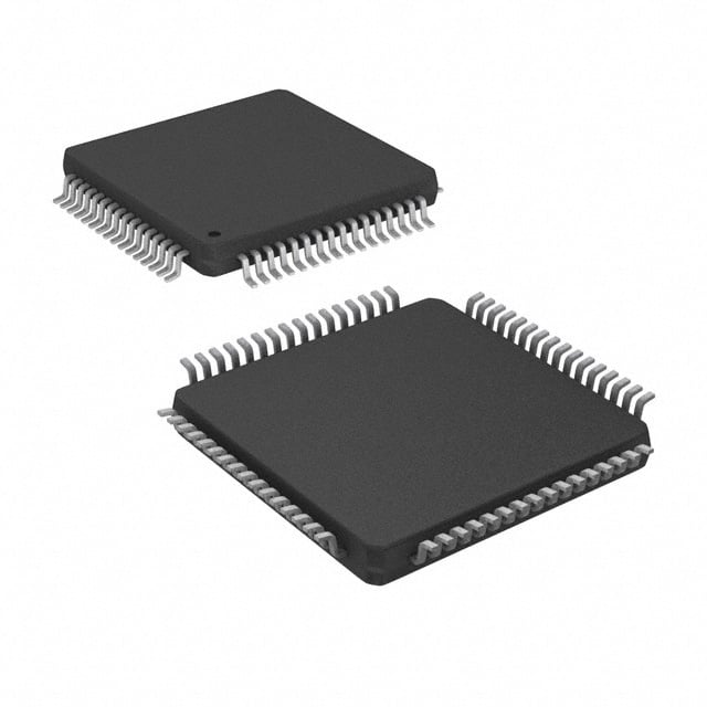
| 供应商器件封装 | 64-TQFP(10x10) |
| 其它名称 | DS92LV3221TVS |
| 功能 | 串行器 |
| 包装 | 托盘 |
| 商标 | Texas Instruments |
| 安装类型 | 表面贴装 |
| 安装风格 | SMD/SMT |
| 封装 | Tray |
| 封装/外壳 | 64-TQFP |
| 封装/箱体 | TQFP-64 |
| 工作温度 | -40°C ~ 85°C |
| 工作温度范围 | - 40 C to + 85 C |
| 工作电源电压 | 3.135 V to 3.465 V |
| 工厂包装数量 | 160 |
| 数据速率 | 1.6 Gbit/s |
| 最大工作温度 | + 85 C |
| 最小工作温度 | - 40 C |
| 标准包装 | 160 |
| 电压-电源 | 3.135 V ~ 3.465 V |
| 类型 | Serializer |
| 系列 | DS92LV3221 |
| 输入数 | 32 |
| 输入端数量 | 32 |
| 输入类型 | LVCMOS |
| 输出数 | 2 |
| 输出端数量 | 2 |
| 输出类型 | LVDS |


PDF Datasheet 数据手册内容提取
DS92LV3221, DS92LV3222 www.ti.com SNLS319C–OCTOBER2009–REVISEDAPRIL2013 DS92LV3221/DS92LV3222 20-50 MHz 32-Bit Channel Link II Serializer / Deserializer CheckforSamples:DS92LV3221,DS92LV3222 FEATURES APPLICATIONS 1 • WideOperatingRangeEmbeddedClock • IndustrialImaging(Machine-vision)and 2 SER/DES Control – Upto32-bitParallelLVCMOSData • SecurityandSurveillanceCamerasand – 20to50MHzParallelClock Infrastructure – Upto1.6GbpsApplicationDataPaylod • MedicalImaging • SimplifiedClockingArchitecture DESCRIPTION – NoSeparateSerialClockLine The DS92LV3221 (SER) serializes a 32-bit data bus – NoReferenceClockRequired into 2 embedded clock LVDS serial channels for a – ReceiverLockstoRandomData data payload rate up to 1.6 Gbps over cables such as CATx, or backplanes FR-4 traces. The companion • On-chipSignalConditioningforRobustSerial DS92LV3222 (DES) deserializes the 2 LVDS serial Connectivity data channels, de-skews channel-to-channel delay – TransmitPre-Emphasis variations and converts the LVDS data stream back – DataRandomization intoa32-bitLVCMOSparalleldatabus. – DC-BalanceEncoding On-chip data Randomization/Scrambling and DC – ReceiveChannelDeskew balance encoding and selectable serializer Pre- emphasis ensure a robust, low-EMI transmission over – Supportsupto10mCAT-5at1.6Gbps longer, lossy cables and backplanes. The • IntegratedLVDSTerminations Deserializer automatically locks to incoming data • Built-inAT-SPEEDBISTforEnd-To-End without an external reference clock or special sync SystemTesting patterns,providinganeasy“plug-and-lock” operation. • AC-CoupledInterconnectforIsolationand By embedding the clock in the data payload and FaultProtection including signal conditioning functions, the Channel- Link II SerDes devices reduce trace count, eliminate • >4KVHBMESDProtection skew issues, simplify design effort and lower • Space-Saving64-pinTQFPPackage cable/connector cost for a wide variety of video, • FullIndustrialTemperatureRange:-40°to control and imaging applications. A built-in AT- +85°C SPEED BIST feature validates link integrity and may beusedforsystemdiagnostics. BLOCKDIAGRAM High-Speed TxCLKIN PLL Serial Data CDR/PLL RxCLKOUT 100:(cid:3)differential pairs TxIN0 RxOUT0 TTTxxxIININN113651 LVCMOS DC Balance Encoder Parallel-to-Serial TTTxxxOOOUUUTTT010 ++- RRRxxxIIINNN001 + -+ Cable Deskew Serial-to-Parallel Decoding, Alignment LVCMOS RRRxxxOOOUUUTTT113561 TxOUT1 - RxIN1 - PDB BIST R_FB BIST LOCK BISTEN MODE REN VPSREEL Control Pre-Emp RP_DFBB Control Tx - SERIALIZER Rx - DESERIALIZER 1 Pleasebeawarethatanimportantnoticeconcerningavailability,standardwarranty,anduseincriticalapplicationsof TexasInstrumentssemiconductorproductsanddisclaimerstheretoappearsattheendofthisdatasheet. Alltrademarksarethepropertyoftheirrespectiveowners. 2 PRODUCTIONDATAinformationiscurrentasofpublicationdate. Copyright©2009–2013,TexasInstrumentsIncorporated Products conform to specifications per the terms of the Texas Instruments standard warranty. Production processing does not necessarilyincludetestingofallparameters.
DS92LV3221, DS92LV3222 SNLS319C–OCTOBER2009–REVISEDAPRIL2013 www.ti.com TopView 3 2 1 0 1 1 1 1 9 8 7 6 5 4 3 2 1 0 N N N N N S D N N N N N N N N N TxI TxI TxI TxI TxI VS VD TxI TxI TxI TxI TxI TxI TxI TxI TxI 8 7 6 5 4 3 2 1 0 9 8 7 6 5 4 3 4 4 4 4 4 4 4 4 4 3 3 3 3 3 3 3 IOVDD 49 32 VDD IOVSS 50 31 VSS TxIN14 51 30 TxOUT0+ TxIN15 52 29 TxOUT0- VDDPLL 53 28 TxOUT1+ VSSPLL 54 27 TxOUT1- VSSPLL 55 DS92LV3221 26 VDDA VDDPLL 56 25 VSSA TxIN16 57 24 NC TxIN17 58 23 NC TxIN18 59 22 NC TxIN19 60 21 NC TxIN20 61 20 VSEL TxIN21 62 19 PRE TxIN22 63 18 VDD TxIN23 64 17 VSS 0 1 2 3 4 5 6 1 2 3 4 5 6 7 8 9 1 1 1 1 1 1 1 4 5 6 7 8 S D 9 0 1 N B N B 1 2 TxIN2 TxIN2 TxIN2 TxIN2 TxIN2 VS VD TxIN2 TxIN3 TxIN3 TxCLKI PD BISTE R_F RSVD RSVD Figure1. DS92LV3221PinDiagram 64-PinTQFP(PAGPackage) 2 SubmitDocumentationFeedback Copyright©2009–2013,TexasInstrumentsIncorporated ProductFolderLinks:DS92LV3221 DS92LV3222
DS92LV3221, DS92LV3222 www.ti.com SNLS319C–OCTOBER2009–REVISEDAPRIL2013 DS92LV3221SerializerPINDESCRIPTIONS Pin# PinName I/O,Type Description LVCMOSPARALLELINTERFACEPINS 10–8, TxIN[31:29], I,LVCMOS SerializerParallelInterfaceDataInputPins. 5–1, TxIN[28:24], 64–57, TxIN[23:16], 52–51, TxIN[15:14], 48–44. TxIN[13:9], 41–33 TxIN[8:0] 11 TxCLKIN I,LVCMOS SerializerParallelInterfaceClockInputPin.StrobeedgesetbyR_FBconfigurationpin. CONTROLANDCONFIGURATIONPINS 12 PDB I,LVCMOS SerializerPowerDownBar(ACTIVELOW) PDB=L;DeviceDisabled,DifferentialserialoutputsareputintoTRI-STATEstand-bymode, PLLisshutdown PDB=H;DeviceEnabled 19 PRE I,LVCMOS PRE-emphasislevelselectpin PRE=(RPRE>12kΩ);Imax=[(1.2/R)x20x2],Rmin=12kΩ. PRE=Horfloating;pre-emphasisisdisabled. 14 R_FB I,LVCMOS Rising/FallingBarClockEdgeSelect R_FB=H;RisingEdge, R_FB=L;FallingEdge 20 VSEL I,LVCMOS VOD(DifferentialOutputVoltage)LlevelSelect VSEL=L;LowSwing, VSEL=H;HighSwing 13 BISTEN I,LVCMOS BISTEnable BISTEN=L;BISTOFF,(default),normaloperatingmode. BISTEN=H;BISTEnabled(ACTIVEHIGH) 15,16 RSVD I,LVCMOS Reserved—MUSTBETIEDLOW 21,22, NC DoNotConnect,leavepinsfloating 23,24 LVDSSERIALINTERFACEPINS 28,30 TxOUT[1:0]+ O,LVDS SerializerLVDSNon-InvertedOutputs(+) 27,29 TxOUT[1:0]- O,LVDS SerializerLVDSInvertedOutputs(-) POWER/GROUNDPINS 7,18,32, VDD VDD DigitalVoltagesupply,3.3V 42 6,17,31, VSS GND Digitalground 43 53,56 VDDPLL VDD AnalogVoltagesupply,PLLPOWER,3.3V 54,55 VSSPLL GND Analogground,PLLGROUND 26 VDDA VDD AnalogVoltagesupply 25 VSSA GND Analogground 49 IOVDD VDD DigitalIOVoltagesupplyConnectto1.8Vtypfor1.8VLVCMOSinterfaceConnectto3.3Vtypfor 3.3VLVCMOSinterface 50 IOVSS GND DigitalIOground Copyright©2009–2013,TexasInstrumentsIncorporated SubmitDocumentationFeedback 3 ProductFolderLinks:DS92LV3221 DS92LV3222
DS92LV3221, DS92LV3222 SNLS319C–OCTOBER2009–REVISEDAPRIL2013 www.ti.com TopView 0 1 0 1 2 3 4 L L 5 6 7 8 9 1 1 T T T T T L L T T T T T T T FB VD OU OU OU OU OU SP DP OU OU OU OU OU OU OU _ S x x x x x S D x x x x x x x R R R R R R R V V R R R R R R R 8 7 6 5 4 3 2 1 0 9 8 7 6 5 4 3 4 4 4 4 4 4 4 4 4 3 3 3 3 3 3 3 PDB 49 32 RxOUT12 REN 50 31 RxOUT13 RxIN0+ 51 30 RxOUT14 RxIN0- 52 29 RxOUT15 RxIN1+ 53 28 RxOUT16 RxIN1- 54 27 VSS VDDA 55 DS92LV3222 26 VDD VSSA 56 25 RxOUT17 NC 57 24 RxOUT18 NC 58 23 RxOUT19 NC 59 22 RxOUT20 NC 60 21 RxOUT21 VDD 61 20 RxOUT22 VSS 62 19 RxOUT23 VSSPLL 63 18 VSS VDDPLL 64 17 VDD 0 1 2 3 4 5 6 1 2 3 4 5 6 7 8 9 1 1 1 1 1 1 1 L L K T 1 0 9 S D 8 7 6 5 4 S D VDDPL VSSPL LOC xCLKOU RxOUT3 RxOUT3 RxOUT2 VS VD RxOUT2 RxOUT2 RxOUT2 RxOUT2 RxOUT2 VS VD R Figure2. DS92LV3222PinDiagram 64-PinTQFP(PAGPackage) 4 SubmitDocumentationFeedback Copyright©2009–2013,TexasInstrumentsIncorporated ProductFolderLinks:DS92LV3221 DS92LV3222
DS92LV3221, DS92LV3222 www.ti.com SNLS319C–OCTOBER2009–REVISEDAPRIL2013 DS92LV3222DESERIALIZERPINDESCRIPTIONS Pin# PinName I/O,Type Description LVCMOSPARALLELINTERFACEPINS 5–7, RxOUT[31:29], O,LVCMOS DeserializerParallelInterfaceDataOutputPins. 10–14, RxOUT[28:24], 19–25, RxOUT[23:17], 28–32, RxOUT[16:12], 33–39, RxOUT[11:5], 42–46 RxOUT[4:0] 4 RxCLKOUT O,LVCMOS DeserializerRecoveredClockOutput.Paralleldatarateclockrecoveredfromtheembedded clock. 3 LOCK O,LVCMOS LOCKindicatesthestatusofthereceiverPLLLOCK=L;deserializerCDR/PLLisnotlocked, RxOUT[31:0]andRCLKareTRI-STATED LOCK=H;deserializerCDR/PLLislocked CONTROLANDCONFIGURATIONPINS 48 R_FB I,LVCMOS Rising/FallingBarClockEdgeSelect R_FB=H;RxOUTclockedonrisingedge R_FB=L;RxOUTclockedonfallingedge 50 REN I,LVCMOS DeserializerEnable,DESOutputEnableControlInput(ACTIVEHIGH) REN=L;disabled,RxOUT[31:0]andRxCLKOUTTRI-STATED,PLLstilloperational REN=H;Enabled(ACTIVEHIGH) 49 PDB I,LVCMOS PowerDownBar,ControlInputSignal(ACTIVELOW) PDB=L;disabled,RxOUT[31:0],RCLK,andLOCKareTRI-STATEDinstand-bymode,PLL isshutdown PDB=H;Enabled 47 RSVD I,LVCMOS Reserved—MUSTBETIEDLOW 57,58, NC DoNotConnect,leavepinsfloating 59,60 LVDSSERIALINTERFACEPINS 51,53 RxIN[0:1]+ I,LVDS DeserializerLVDSNon-InvertedInputs(+) 52,54 RxIN[0:1]- I,LVDS DeserializerLVDSInvertedInputs(-) POWER/GROUNDPINS 9,16, VDD VDD DigitalVoltagesupply,3.3V 17,26, 61 8,15, VSS GND DigitalGround 18,27, 62 55 VDDA VDD AnalogLVDSVoltagesupply,POWER,3.3V 56 VSSA GND AnalogLVDSGROUND 1,40, VDDPLL VDD AnalogVoltagesupplyPLLVCOPOWER,3.3V 64 2,41, VSSPLL GND Analogground,PLLVCOGROUND 63 Copyright©2009–2013,TexasInstrumentsIncorporated SubmitDocumentationFeedback 5 ProductFolderLinks:DS92LV3221 DS92LV3222
DS92LV3221, DS92LV3222 SNLS319C–OCTOBER2009–REVISEDAPRIL2013 www.ti.com Thesedeviceshavelimitedbuilt-inESDprotection.Theleadsshouldbeshortedtogetherorthedeviceplacedinconductivefoam duringstorageorhandlingtopreventelectrostaticdamagetotheMOSgates. ABSOLUTE MAXIMUM RATINGS(1)(2) SupplyVoltage(V ) −0.3Vto+4V DD LVCMOSInputVoltage −0.3Vto(V +0.3V) DD LVCMOSOutputVoltage −0.3Vto(V +0.3V) DD LVDSDeserializerInputVoltage −0.3Vto+3.9V LVDSDriverOutputVoltage −0.3Vto+3.9V JunctionTemperature +125°C StorageTemperature −65°Cto+150°C LeadTemperature(Soldering,4seconds) +260°C MaximumPackagePowerDissipationCapacityPackageDerating 1/θ °C/Wabove+25°C JA θ 35.7°C/W(3) JA θ 12.6°C/W JC ESDRating(HBM) >4kV (1) IfMilitary/Aerospacespecifieddevicesarerequired,pleasecontacttheTexasInstrumentsSalesOffice/Distributorsforavailabilityand specifications. (2) “AbsoluteMaximumRatings”indicatelimitsbeyondwhichdamagetothedevicemayoccur,includinginoperabilityanddegradationof devicereliabilityand/orperformance.Functionaloperationofthedeviceand/ornon-degradationattheAbsoluteMaximumRatingsor otherconditionsbeyondthoseindicatedintheRecommendedOperatingConditionsisnotimplied.TheRecommendedOperating Conditionsindicateconditionsatwhichthedeviceisfunctionalandthedeviceshouldnotbeoperatedbeyondsuchconditions. (3) 4LayerJEDEC RECOMMENDED OPERATING CONDITIONS Min Nom Max Units SupplyVoltage(V ) 3.135 3.3 3.465 V DD SupplyVoltage(IOV ) 3.3VI/OInterface 3.135 3.3 3.465 V DD (SERONLY) 1.8VI/OInterface 1.71 1.8 1.89 V OperatingFreeAirTemperature(T ) −40 +25 +85 °C A InputClockRate 20 50 MHz TolerableSupplyNoise 100 mV P-P ELECTRICAL CHARACTERISTICS Overrecommendedoperatingsupplyandtemperaturerangesunlessotherwisespecified.(1)(2) Symbol Parameter Conditions Min Typ Max Units LVCMOSDCSPECIFICATIONS V HighLevelInputVoltage Tx:IOV =1.71Vto1.89V 0.65x IOV + IH DD DD IOV 0.3 DD V Tx:IOV =3.135Vto3.465V DD 2.0 V DD Rx V LowLevelInputVoltage Tx:IOV =1.71Vto1.89V 0.35x IL DD GND IOV DD V Tx:IOV =3.135Vto3.465V DD GND 0.8 Rx V InputClampVoltage I =−18mA −0.8 −1.5 V CL CL I InputCurrent Tx:V =0Vor3.465V(1.89V) IN IN −10 +10 IOVDD=3.465V(1.89V) µA Rx:V =0Vor3.465V −10 +10 IN (1) TypicalvaluesrepresentmostlikelyparametricnormsatV =3.3V,T =+25°C,andattheRecommendedOperatingConditionsat DD A thetimeofproductcharacterizationandarenotverified. (2) Currentintoathedeviceisdefinedaspositive.Currentoutofadevicepinisdefinedasnegative.Voltagesarereferencedtoground exceptV ,ΔV ,V ,V whicharedifferentialvoltages. OD OD TH TL 6 SubmitDocumentationFeedback Copyright©2009–2013,TexasInstrumentsIncorporated ProductFolderLinks:DS92LV3221 DS92LV3222
DS92LV3221, DS92LV3222 www.ti.com SNLS319C–OCTOBER2009–REVISEDAPRIL2013 ELECTRICAL CHARACTERISTICS (continued) Overrecommendedoperatingsupplyandtemperaturerangesunlessotherwisespecified.(1)(2) Symbol Parameter Conditions Min Typ Max Units V HighLevelOutputVoltage I =−2mA 2.4 3.0 V V OH OH DD V LowLevelOutputVoltage I =−2mA GND 0.33 0.5 V OL OH I OutputShortCircuitCurrent V =0V −22 −40 mA OS OUT I TRI-STATEOutputCurrent PDB=0V, OZ −10 +10 μA V =0VorV OUT DD SERIALIZERLVDSDCSPECIFICATIONS V OutputDifferentialVoltage Nopre-emphasis,VSEL=L 350 440 525 OD mV (VSEL=H) (629) (850) (1000) P-P ΔV OutputDifferentialVoltageUnbalance VSEL=L,Nopre-emphasis 1 50 mV OD P-P V OffsetVoltage VSEL=L,Nopre-emphasis 1.00 1.25 1.50 V OS ΔV OffsetVoltageUnbalance VSEL=L,Nopre-emphasis 4 50 mV OS I OutputShortCircuitCurrent TxOUT[1:0]=0V,PDB=V , OS DD −2 −5 VSEL=L,Nopre-emphasis mA TxOUT[1:0]=0V,PDB=V , DD −6 −10 VSEL=H,Nopre-emphasis I TRI-STATEOutputCurrent PDB=0V,TxOUT[1:0]=0VORV −15 ±1 +15 µA OZ DD PDB=V ,TxOUT[1:0]=0VORV −15 ±1 +15 µA DD DD R OutputTermination Internaldifferentialoutputtermination T 90 100 130 Ω betweendifferentialpairs SERIALIZERSUPPLYCURRENT(DVDD,PVDDANDAVDDPINS)(3) I Serializer(Tx)TotalSupplyCurrent f=50MHz,CHECKERBOARDpattern DDTD 120 145 (includesloadcurrent) VSEL=H,PRE=OFF f=50MHz,CHECKERBOARDpattern 120 145 VSEL=H,RPRE=12kΩ mA f=50MHz,RANDOMpattern 115 135 VSEL=H,PRE=OFF f=50MHz,RANDOMpattern 115 135 VSEL=H,RPRE=12kΩ I SerializerSupplyCurrent TPWDNB=0V DDTZ 2 50 µA Power-down (AllotherLVCMOSInputs=0V) DESERIALIZERLVDSDCSPECIFICATIONS V DifferentialThresholdHighVoltage V =+1.8V +50 mV TH CM V DifferentialThresholdLowVoltage −50 mV TL R InputTermination Internaldifferentialoutputtermination T 90 100 130 Ω betweendifferentialpairs I InputCurrent V =+2.4V,V =3.6V ±100 ±250 µA IN IN DD V =0V,V =3.6V ±100 ±250 µA IN DD DESERIALIZERSUPPLYCURRENT(DVDD,PVDDANDAVDDPINS)(3) f=50MHz,C =8pF, L 145 185 CHECKERBOARDpattern mA f=50MHz,C =8pF, L 122 140 RANDOMpattern I DeserializerSupplyCurrentPower-down PDB=0V DDRZ (AllotherLVCMOSInputs=0V, 100 µA RxIN[1:0](P/N)=0V) (3) DIGITAL,PLL,ANDANALOGVDDS Copyright©2009–2013,TexasInstrumentsIncorporated SubmitDocumentationFeedback 7 ProductFolderLinks:DS92LV3221 DS92LV3222
DS92LV3221, DS92LV3222 SNLS319C–OCTOBER2009–REVISEDAPRIL2013 www.ti.com SERIALIZER INPUT TIMING REQUIREMENTS FOR TCLK Overrecommendedoperatingsupplyandtemperaturerangesunlessotherwisespecified. Symbol Parameter Conditions Min Typ Max Units t TxCLKINPeriod 20 t 50 ns CIP CIP t TxCLKINHighTime 20MHz–50MHz 0.45x 0.55x CIH 0.5xt ns t CIP t CIP CIP t TxCLKINLowTime 20MHz–50MHz 0.45x 0.55x TCIL 0.5xt ns Figure5 t CIP t CIP CIP t TxCLKINTransitionTime 20MHz–50MHz CIT 0.5 1.2 ns Figure4 t TxCLKINJitter ±100 ps JIT P-P SERIALIZER SWITCHING CHARACTERISTICS Overrecommendedoperatingsupplyandtemperaturerangesunlessotherwisespecified. Symbol Parameter Conditions Min Typ Max Units t LVDSLow-to-HighTransitionTime Nopre-emphasis 350 ps LLHT Figure3 t LVDSHigh-to-LowTransitionTime 350 ps LHLT t TxIN[31:0]SetuptoTxCLKIN IOVDD=1.71Vto1.89V STC 0 Figure5 ns IOVDD=3.135Vto3.465V 0 t TxIN[31:0]HoldfromTxCLKIN IOVDD=1.71Vto1.89V 2.5 HTC ns IOVDD=3.135Vto3.465V 2.25 t SerializerPLLLockTime Figure7 4400x 5000x PLD ns t t CIP CIP t DataOutputLOWtoTRI-STATE See(1) LZD 5 10 ns Delay t DataOutputTRI-STATEtoHIGH See(1) HZD 5 10 ns Delay t SerializerPropagationDelay-Latency f=50MHz,R_FB=H, SD 4.5t + PRE=OFF, CIP 6.77 Figure6 f=50MHz,R_FB=L, 4.5t + 4.5t + 4.5t + ns PRE=OFF, CIP CIP CIP 5.63 7.09 9.29 Figure6 f=20MHz,R_FB=H, 4.5t + 4.5t + 4.5t + CIP CIP CIP PRE=OFF, 6.57 8.74 10.74 t LVDSOutputSkew LVDSdifferentialoutputchannel-to- LVSKD 30 500 ps channelskew Λ JitterTransferFunction-3dB f=50MHz STXBW 2.8 MHz Bandwidth Figure13 δ SerializerJitterTransferFunction f=50MHz STX 0.3 dB Peaking (1) WhentheSerializeroutputisatTRI-STATEtheDeserializerwilllosePLLlock.ResynchronizationMUSToccurbeforedatatransfer. 8 SubmitDocumentationFeedback Copyright©2009–2013,TexasInstrumentsIncorporated ProductFolderLinks:DS92LV3221 DS92LV3222
DS92LV3221, DS92LV3222 www.ti.com SNLS319C–OCTOBER2009–REVISEDAPRIL2013 DESERIALIZER SWITCHING CHARACTERISTICS Overrecommendedoperatingsupplyandtemperaturerangesunlessotherwisespecified. Symbol Parameter Conditions Min Typ Max Units t ReceiverOutputClockPeriod t =t ROCP ROCP CIP 20 t 50 ns Figure9 ROCP t RxCLKOUTDutyCycle 45 50 55 % RODC t LVCMOSLow-to-HighTransition C =8pF ROTR L 3.2 ns Time (lumpedload) Figure8 t LVCMOSHigh-to-LowTransition ROTF 3.5 ns Time t RxOUT[31:0]SetuptoRxCLKOUT f=50MHz 0.5x ROSC 5.6 ns t ROCP t RxOUT[31:0]HoldtoRxCLKOUT 0.5x ROHC 7.4 ns t ROCP t DataOutputHightoTRI-STATE Figure11 HZR 5 10 ns Delay t DataOutputLowtoTRI-STATE LZR 5 10 ns Delay t DataOutputTRI-STATEtoHigh ZHR 5 10 ns Delay t DataOutputTRI-STATEtoLow ZLR 5 10 ns Delay t DeserializerPorpagationDelay– 5.5x ns RD f=20MHz Latency t + Figure10 ROCP 3.35 5.5x ns f=50MHz t + ROCP 6.00 t DeserializerPLLLockTime 20MHz–50MHz RPLLS 128kx Figure11 ns See(1) tROCP TOL DeserializerInputJitterTolerance 0.25 UI JIT t LVDSDifferentialInputSkew 20MHz–50MHz 0.4x LVSKR ns Tolerance Figure15 t ROCP (1) t isthetimerequiredbytheDeserializertoobtainlockwhenexitingpower-downmode. RPLLS Copyright©2009–2013,TexasInstrumentsIncorporated SubmitDocumentationFeedback 9 ProductFolderLinks:DS92LV3221 DS92LV3222
DS92LV3221, DS92LV3222 SNLS319C–OCTOBER2009–REVISEDAPRIL2013 www.ti.com AC Timing Diagrams and Test Circuits Differential 80% 80% Signal Vdiff = 0V 20% 20% tLLHT tLHLT Figure3. SerializerLVDSTransitionTimes VDDIO 80% 80% TxCLKIN 20% 20% 0V tCIT tCIT Figure4. SerializerInputClockTransitionTime tCIP TxCLKIN tCIH + tCIL tSTC tHTC TxIN Setup Hold Figure5. SerializerSetup/HoldandHigh/LowTimes | | | | | TxIN SYMBOL N-1 SYMBOL N SYMBOL N+1 SYMBOL N+2 SYMBOL N+3 | | | | | | TxCLKIN tSD SYMBOL N-3 SYMBOL N-2 SYMBOL N-1 SYMBOL N SYMBOL N+1 | | | | | TxOUT | | | | | Figure6. SerializerPropagationDelay 10 SubmitDocumentationFeedback Copyright©2009–2013,TexasInstrumentsIncorporated ProductFolderLinks:DS92LV3221 DS92LV3222
DS92LV3221, DS92LV3222 www.ti.com SNLS319C–OCTOBER2009–REVISEDAPRIL2013 PDB 2.0V 0.8V tHZD or tLZD TxCLKIN tPLD TxOUT TRI-STATE LVDS Output HIGH LVDS Output Active TRI-STATE Figure7. SerializerPLLLockTime VOH 80% 80% 20% 20% VOL tROTR tROTF Figure8. DeserializerLVCMOSOutputTransitionTime tROCP tRODC tRODC RxCLKOUT VDD/2 VDD/2 tROSC tROHC Data Valid Data Valid RxOUT [31:0] VDD/2 Before After VDD/2 RxCLKOUT RxCLKOUT Figure9. DeserializerSetupandHoldtimes SYMBOL N-1 SYMBOL N SYMBOL N+1 SYMBOL N+2 SYMBOL N+3 | | | | | RxIN | | | | | tRD | RxCLKOUT | | | | | RxOUT SYMBOL N-3 SYMBOL N-2 SYMBOL N-1 SYMBOL N SYMBOL N +1 | | | | | Figure10. DeserializerPropagationDelay Copyright©2009–2013,TexasInstrumentsIncorporated SubmitDocumentationFeedback 11 ProductFolderLinks:DS92LV3221 DS92LV3222
DS92LV3221, DS92LV3222 SNLS319C–OCTOBER2009–REVISEDAPRIL2013 www.ti.com PDB 2.0V 0.8V tRPLLS | RxIN [1:0]+/- ’RQ¶W(cid:3)&DUH | LOCK TRI-STATE TRI-STATE tHZR or tLZR RxOUT [31:0] TRI-STATE TRI-STATE RxCLKOUT TRI-STATE TRI-STATE REN Figure11. DeserializerPLLLockTimeandPDBTRI-STATEDelay 500: VREF VREF = VDD/2 for tZLR or tLZR + CL = 8 pF - VREF = 0V for tZHR or tHZR REN VOH REN VDD/2 VDD/2 VOL tLZR tZLR VOL + 0.5V VOL + 0.5V VOL RxOUT [31:0] tHZR tZHR VOH VOH - 0.5V VOH + 0.5V Note: CL includes instrumentation and fixture capacitance within 6 cm of RxOUT [31:0]. Figure12. DeserializerTRI_STATETestCircuitandTiming 0 TxCLKIN = 50 MHz B) -3 d N ( AI G -6 -9 1.0E+021.0E+03 1.0E+04 1.0E+05 1.0E+06 1.0E+07 FREQUENCY (Hz) Figure13. SerializerJitterTransfer 12 SubmitDocumentationFeedback Copyright©2009–2013,TexasInstrumentsIncorporated ProductFolderLinks:DS92LV3221 DS92LV3222
DS92LV3221, DS92LV3222 www.ti.com SNLS319C–OCTOBER2009–REVISEDAPRIL2013 L A IR E TxOUT[1:0]+ S 32 O- TxIN T-L RT RL E L LA TxOUT[1:0]- R A P TxCLKIN Figure14. SerializerV TestCircuitDiagram OD tLVSKR RxIN0 1K 0K (Master) LC LC 1 0 RxIN1 KL KL C C 1 RxCLKOUT Cycle RxCLKOUT Figure15. LVDSDeserializerInputSkew Copyright©2009–2013,TexasInstrumentsIncorporated SubmitDocumentationFeedback 13 ProductFolderLinks:DS92LV3221 DS92LV3222
DS92LV3221, DS92LV3222 SNLS319C–OCTOBER2009–REVISEDAPRIL2013 www.ti.com FUNCTIONAL DESCRIPTION The DS92LV3221 Serializer (SER) and DS92LV3222 Deserializer (DES) chipset is a flexible SER/DES chipset that translates a 32-bit parallel LVCMOS data bus into 2 pairs of LVDS serial links with embedded clock. The DS92LV3221 serializes the 32-bit wide parallel LVCMOS word into two high-speed LVDS serial data streams with embedded clock, scrambles and DC Balances the data to support AC coupling and enhance signal quality. The DS92LV3222 receives the dual LVDS serial data streams and converts it back into a 32-bit wide parallel data with a recovered clock. The dual LVDS serial data stream reduces cable size, the number of connectors, andeasesskewconcerns. Parallel clocks between 20 MHz to 50 MHz are supported. The embedded clock LVDS serial streams have an effective data payload of 640 Mbps (20MHz x 32-bit) to 1.6 Gbps (50MHz x 32- bit). The SER/DES chipset is designed to transmit data over long distances through standard twisted pair (TWP) cables. The differential inputs and outputs are internally terminated with 100 ohm resistors to provide source and load termination, minimize stublength,toreducecomponentcountandfurtherminimizeboardspace. The DES can attain lock to a data stream without the use of a separate reference clock source; greatly simplifying system complexity and reducing overall cost. The DES synchronizes to the SER regardless of data pattern, delivering true automatic “plug-and-lock” performance. It will lock to the incoming serial stream without the need of special training patterns or special sync characters. The DES recovers the clock and data by extractingtheembeddedclockinformation,deskewstheserialdatachannelsandthendeserializesthedata.The DES also monitors the incoming clock information, determines lock status, and asserts the LOCK output high when lock occurs. In addition the DES also supports an optional AT-SPEED BIST (Built In Self Test) mode, BIST error flag, and LOCK status reporting pin. The SER and the DES have a power down control signal to enable efficientoperationinvariousapplications. DESKEW AND CHANNEL ALIGNMENT The DES automatically provides a clock alignment and deskew function without the need for any special training patterns. During the locking phase, the embedded clock information is recovered on all channels and the serial links are internally synchronized, de-skewed, and auto aligned. The internal CDR circuitry will dynamically compensate for up to 0.4 times the parallel clock period of per channel phase skew (channel-to-channel) between the recovered clocks of the serial links. This provides skew phase tolerance from mismatches in interconnectwiressuchasPCBtracerouting,cablepair-to-pairlengthdifferences,andconnectorimbalances. DATA TRANSFER After SER lock is established (SER PLL to TxCLKIN), the inputs TxIN0–TxIN31 are latched into the encoder block. Data is clocked into the SER by the TxCLKIN input. The edge of TxCLKIN used to strobe the data is selectable via the R_FB (SER) pin. R_FB (SER) high selects the rising edge for clocking data and low selects the falling edge. The SER outputs (TxOUT[1:0]+/-) are intended to drive a AC Coupled point-to-point connections. The SER latches 32-bit parallel data bus and performs several operations to it. The 32-bit parallel data is internally encoded and sequentially transmitted over the two high-speed serial LVDS channels. For each serial channel, the SER transmits 20 bits of information per payload to the DES. This results in a per channel throughputof400Mbpsto1.0Gbps(20bitsxclockrate). When all of the DES channels obtain lock , the LOCK pin is driven high and synchronously delivers valid data and recovered clock on the output. The DES locks to the clock, uses it to generate multiple internal data strobes, and then drives the recovered clock to the RxCLKOUT pin. The recovered clock (RxCLKOUT) is synchronous to thedataontheRxOUT[31:0]pins.WhileLOCKishigh,dataonRxOUT[31:0]isvalid.Otherwise,RxOUT[31:0]is invalid. The polarity of the RxCLKOUT edge is controlled by its R_FB (DES) input. RxOUT[31:0], LOCK and RxCLKOUT outputs will each drive a maximum of 8 pF load. REN controls TRI-STATE for RxOUT0–RxOUT31 andtheRxCLKOUTpinontheDES. 14 SubmitDocumentationFeedback Copyright©2009–2013,TexasInstrumentsIncorporated ProductFolderLinks:DS92LV3221 DS92LV3222
DS92LV3221, DS92LV3222 www.ti.com SNLS319C–OCTOBER2009–REVISEDAPRIL2013 RESYNCHRONIZATION IntheabsenceofdatatransitionsononeofthechannelsintotheDES(e.g.alossofthelink),itwillautomatically try to resynchronize and re-establish lock using the standard lock sequence on the master channel (Channel 0). Forexample,iftheembeddedclockisnotdetectedonetimeinsuccessiononeitheroftheseriallinks,theLOCK pin is driven low. The DES then monitors the master channel for lock, once that is obtained, the second channel is locked and aligned. The logic state of the LOCK signal indicates whether the data on RxOUT is valid; when it is high, the data is valid. The system may monitor the LOCK pin to determine whether data on the RxOUT is valid. POWERDOWN ThePowerdownstateisalowpowersleepmodethattheSERandDESmayusetoreducepowerwhennodata isbeingtransferred.TherespectivePDBpinsareusedtoseteachdeviceintopowerdownmode,whichreduces supply current into the µA range. The SER enters Powerdown when the SER PDB pin is driven low. In Powerdown, the PLL stops and the outputs go into TRI-STATE, disabling load current and reducing current supply. To exit Powerdown, SER PDB must be driven high. When the SER exits Powerdown, its PLL must lock to TxCLKIN before it is ready for sending data to the DES. The system must then allow time for the DES to lock beforedatacanberecovered. The DES enters Powerdown mode when DES PDB is driven low. In Powerdown mode, the PLL’s stop and the outputsenterTRI-STATE.TobringtheDESblockoutofthePowerdownstate,thesystemdrivesDESPDBhigh. Both the SER and DES must relock before data can be transferred from Host and received by the Target. The DESwillstartupandassertLOCKhighwhenitislockedtotheembeddedclocks.SeealsoFigure11. TRI-STATE For the SER, TRI-STATE is entered when the SER PDB pin is driven low. This will TRI-STATE the driver output pinsonTxOUT[1:0]+/-. When you drive the REN or DES PDB pin low, the DES output pins (RxOUT[31:0]) and RxCLKOUT will enter TRI-STATE. The LOCK output remains active, reflecting the state of the PLL. The DES input pins are high impedanceduringreceiverPowerdown(DESPDBlow)andpower-off(VDD=0V).SeealsoFigure11. TRANSMIT PARALLEL DATA AND CONTROL INPUTS The DS92LV3221 operates on a core supply voltage of 3.3V with an optional digital supply voltage for 1.8V, low- swing, input support. The SER single-ended (32-bit parallel data and control inputs) pins are 1.8V and 3.3V LVCMOS logic level compatible and is configured through the IOVDD input supply rail. If 1.8V is required, the IOVDD pin must be connected to a 1.8V supply rail. Also when power is applied to the transmitter, IOVDD pin must be applied before or simultaneously with other power supply pins (3.3V). If 1.8V input swing is not required, this pin should be tied to the common 3.3V rail. During normal operation, the voltage level on the IOVDD pins mustnotchange. PRE-EMPHASIS The SER LVDS Line Driver features a Pre-Emphasis function used to compensate for extra long or lossy transmission media. The same amount of Pre-Emphasis is applied on all of the differential output channels. Cable drive is enhanced with a user selectable Pre-Emphasis feature that provides additional output current during transitions to counteract cable loading effects. The transmission distance will be limited by the loss characteristicsandqualityofthemedia. To enable the Pre-Emphasis function, the “PRE” pin requires one external resistor (Rpre) to VSS (GND) in order tosetthepre-emphasizedcurrentlevel.Optionsinclude: 1. NormalOutput(noPre-emphasis)–LeavethePREpinopen,includeanRpad,donotpopulate. 2. EnhancedOutput(Pre-emphasisenabled)– connectaresistoronthePREpintoVss. Values of the Rpre Resistor should be between 12K Ohm and 100K Ohm. Values less than 6K Ohm should not be used. The amount of Pre-Emphasis for a given media will depend on the transmission distance and Fmax of the application. In general, too much Pre-Emphasis can cause over or undershoot at the receiver input pins. This can result in excessive noise, crosstalk, reduced Fmax, and increased power dissipation. For shorter cables or distances, Pre-Emphasis is typically not be required. Signal quality measurements should be made at the end of theapplicationcabletoconfirmtheproperamountofPre-Emphasisforthespecificapplication. Copyright©2009–2013,TexasInstrumentsIncorporated SubmitDocumentationFeedback 15 ProductFolderLinks:DS92LV3221 DS92LV3222
DS92LV3221, DS92LV3222 SNLS319C–OCTOBER2009–REVISEDAPRIL2013 www.ti.com The Pre-Emphasis circuit increases the drive current to I = 48 / (R ). For example if R = 15 kOhms, then PRE PRE thecurrentisincreasedbyanadditional3.2mA.TocalculatetheexpectedincreaseinV ,multiplytheincrease OD incurrentby50ohms.SoforthecaseofR =15 kOhms, the boost to V would be 3.2 mA x 50 Ohms = 160 PRE OD mV. The duration of the current is controlled to one bit by time. If more than one bit value is repeated in the next cycle(s), the Pre-Emphasis current is turned off (back to the normal output current level) for the next bit(s). To boost high frequency data and pre-equalize teh data patternreduce ISI (Inter-Symbol Interference) improving the resultingeyepattern. V SELECT OD The SER Line Driver Differential Output Voltage (V ) magnitude is selectable. Two levels are provided and are OD selected by the VSEL pin. When this pin is LOW, normal output levels are obtained. For most application set the VSEL pin LOW. When this pin is HIGH, the output current is increased to double the V level. Use this setting OD onlyforextralongcablesorhigh-lossinterconnects. Table1.V Control OD VSELPinSetting Effect LOW SmallV ,typ440mV OD P-P HIGH LargeV ,typ850mV OD P-P SERIALINTERFACE The serial links between the DS92LV3221 and the DS92LV3222 are intended for a balanced 100 Ohm interconnects.ThelinksmustbeconfiguredasanACcoupledinterface. The SER and DES support AC-coupled interconnects through an integrated DC balanced encoding/decoding scheme. An external AC coupling capacitors must be placed, in series, in the LVDS signal path. The DES input stage is designed for AC-coupling by providing a built-in AC bias network which sets the internal common mode voltage(VCM)to+1.8V. For the high-speed LVDS transmission, small footprint packages should be used for the AC coupling capacitors. This will help minimize degradation of signal quality due to package parasitics. NPO class 1 or X7R class 2 type capacitors are recommended. 50 WVDC should be the minimum used for best system-level ESD performance. The most common used capacitor value for the interface is 100 nF (0.1 uF) capacitor. One set of capacitors may be used for isolation. Two sets (both ends) may also be used for maximum isolation of both the SER and DES fromcablefaults. The DS92LV3221 and the DS92LV3222 differential I/O’s are internally terminated with 100 Ohm resistance between the inverting and non-inverting pins and do not require external termination. The internal resistance value will be between 90 ohm and 130 ohm. The integrated terminations improve signal integrity, reduce stub lengths,anddecreasetheexternalcomponentcountresultinginspacesavings. AT-SPEEDBISTFEATURE The DS92LV3221/ DS92LV3222 serial link is equipped with built-in self-test (BIST) capability to support both system manufacturing and field diagnostics. BIST mode is intended to check the entire high-speed serial interface at full link-speed without the use of specialized and expensive test equipment. This feature provides a simple method for a system host to perform diagnostic testing of both SER and DES. The BIST function is easily configured through the SER BISTEN pin. When the BIST mode is activated, the SER generates a PRBS (pseudo-random bit sequence) pattern (2^7-1). This pattern traverses each lane to the DES input. The DS92LV3222 includes an on-chip PRBS pattern verification circuit that checks the data pattern for bit errors and reportsanyerrorsonthedataoutputpinsoftheDES. The AT-Speed BIST feature is enabled by setting the BISTEN to High on SER. The BISTEN input must be High or Low for 4 or more TxCLKIN clock cycles in order to activate or deactivate the BIST mode. An input clock signal for the Serializer TxCLKIN must also be applied during the entire BIST operation. Once BIST is enabled, alltheSerializerdatainputs(TxIN[31:0])areignoredandtheDESoutputs(RxOUT[31:0])arenotavailable.Next, the internal test pattern generator for each channel starts transmission of the BIST pattern from SER to DES. The DES BIST mode will be automatically activated by this sequence. A maximum of 128 consecutives clock symbols on DS92LV3222 DES is needed to detect BIST enable function. The BIST is implemented with independent transmit and receive paths for the two serial links. Each channel on the DES will be individually comparedagainsttheexpectedbitsequenceoftheBISTpattern. 16 SubmitDocumentationFeedback Copyright©2009–2013,TexasInstrumentsIncorporated ProductFolderLinks:DS92LV3221 DS92LV3222
DS92LV3221, DS92LV3222 www.ti.com SNLS319C–OCTOBER2009–REVISEDAPRIL2013 TxCLKIN PDB (High) 2.0V BISTEN 0.8V BIST disabled BIST enabled BIST disabled 4 x tCIP 4 x tCIP Figure16. BISTTestEnabled/Disabled Under the BIST mode, the DES parallel outputs on RxOUT[31:0] are multiplexed to represent BIST status indicators. The pass/fail status of the BIST is represented by a Pass flag along with an Error counter. The Pass flagoutputisdesignatedonDESRxOUT0forChannel0,andRxOUT16forChannel1.TheDES'sPLLmustfirst belockedtoensurethePassstatusisvalid.TheoutputPassstatuspinwillstayLOWandthentransitiontoHigh once 44*10^6 symbols are achieved across each of the respective transmission links. The total time duration of the test is defined by the following: 44*10^6 x tCIP . After the Pass output flags reach a HIGH state, it will not drop to LOW even if subsequent bit errors occurred after the BIST duration period. Errors will be reported if the input test pattern comparison does not match. If an error (miss-compare) occurs, the status bit is latched on RxOUT[7:1] for Channel 0, and RxOUT[23:17] for Channel 1; reflecting the number of errors detected. Whenever a data bit contains an error, the Error counter bit output for that corresponding channel goes HIGH. Each counter fortheseriallinkutilizesa7-bitcountertostorethenumberoferrorsdetected(0to127max). Copyright©2009–2013,TexasInstrumentsIncorporated SubmitDocumentationFeedback 17 ProductFolderLinks:DS92LV3221 DS92LV3222
DS92LV3221, DS92LV3222 SNLS319C–OCTOBER2009–REVISEDAPRIL2013 www.ti.com Recovered Pixel Clock BISTEN Case 1: No bit errors Start Pixel Recovered Pixel Data Channel 0 - RxOUT0 Copy of Channel 0 - RxOUT8 Channel 1 – RxOUT16 BIST PASS Copy of Channel 1 – RxOUT24 Error counter Channel 0 - RxOUT[7:1] Copy of Channel 0 - RxOUT[15:9] 0 0 0 Channel 1 - RxOUT[23:17] Copy of Channel 1 - RxOUT[31:25] Case 2: Bit error(s) Recovered Pixel Data B B B B Channel 0 - RxOUT0 Copy of Channel 0 - RxOUT8 BIST FAIL Channel 1 – RxOUT16 Copy of Channel 1 – RxOUT24 Error counter Channel 0 - RxOUT[7:1] Copy of Channel 0 - RxOUT[15:9] 0 1 2 3 4 4 Channel 1 - RxOUT[23:17] Copy of Channel 1 - RxOUT[31:25] Case 3: Bit error(s) Recovered Pixel Data B Channel 0 - RxOUT0 Copy of Channel 0 - RxOUT8 Channel 1 – RxOUT16 BIST PASS Copy of Channel 1 – RxOUT24 Error counter Channel 0 - RxOUT[7:1] Copy of Channel 0 - RxOUT[15:9] 0 0 0 Channel 1 - RxOUT[23:17] Copy of Channel 1 - RxOUT[31:25] BIST Duration Status B = Bad Bit 44 x 106 x tCIP Region Figure17. BISTDiagramforDifferentBitErrorCases 18 SubmitDocumentationFeedback Copyright©2009–2013,TexasInstrumentsIncorporated ProductFolderLinks:DS92LV3221 DS92LV3222
DS92LV3221, DS92LV3222 www.ti.com SNLS319C–OCTOBER2009–REVISEDAPRIL2013 TYPICAL APPLICATION CONNECTION Figure 18 shows a typical application of the DS92LV3221 Serializer (SER). The differential outputs utilize 100nF coupling capacitors to the serial lines. Bypass capacitors are placed near the power supply pins. A system GPO (General Purpose Output) controls the PDB and BISTEN pins. In this application the R_FB (SER) pin is tied Low tolatchdataonthefallingedgeoftheTxCLKIN.Inthisapplicationthelinkisshort,thereforetheVSELpinistied LOW for the standard output swing level. The Pre-emphasis input utilizes a resistor to ground to set the amount ofpre-emphasisdesiredbytheapplication. ConfigurationpinsforthetypicalapplicationareshownforSER: • PDB– PowerDownControlInput– ConnecttohostortieHIGH(alwaysON) • BISTEN–ModeInput-tieLOWifBISTmodeisnotused,orconnecttohost • VSEL– tieLOWfornormalVOD(applicationdependant) • PRE– Leaveopenifnotrequired(haveaRpadoptiononPCB) • RSVD1& RSVD2– tieLOW There are eight power pins for the device. These may be bussed together on a common 3.3V plane (3.3V LVCMOS I/O interface). If 1.8V input swing level for parallel data and control pins are required, connect the IOVDDpinto1.8V.Ataminimum,eight0.1uFcapacitorsshouldbeusedforlocalbypassing. Copyright©2009–2013,TexasInstrumentsIncorporated SubmitDocumentationFeedback 19 ProductFolderLinks:DS92LV3221 DS92LV3222
DS92LV3221, DS92LV3222 SNLS319C–OCTOBER2009–REVISEDAPRIL2013 www.ti.com 3.3V VDDA VDD 3.3V 3.3V VDDPLL VDD VDDPLL VDD 1.8V or 3.3V IOVDD VDD TxCLKIN VSS VSS TxIN31 VSS TxIN30 VSS TxIN29 TxIN28 VSSPLL TxIN27 VSSPLL TxIN26 TxIN25 VSSA TxIN24 TxIN23 IOVSS ock TxIN22 Cl TxIN21 us + TxIN20 B TxIN19 a at TxIN18 D MOS TTxxIINN1176 TTxxOOUUTT00+- LVDS 2-bit LVC TTTxxxIIINNN111543 TTxxOOUUTT11+- Serial 3 TxIN12 TxIN11 TxIN10 TxIN9 TxIN8 TxIN7 TxIN6 TxIN5 PRE TxIN4 opt. TxIN3 TxIN2 TxIN1 R_FB TxIN0 VSEL ntrol PDB Co BISTEN RSVD1 RSVD2 Notes: Caps are 0.1 PF except Bulk Supply (4.7 PF) Figure18. DS92LV3221TypicalConnectionDiagram Figure19showsatypicalapplicationoftheDS92LV3222Deserializer(DES).Thedifferentialinputsutilize100nF coupling capacitors in the serial lines. Bypass capacitors are placed near the power supply pins. A system GPO (General Purpose Output) controls the PDB pin. In this application the R_FB (DES) pin is tied Low to strobe the dataonthefallingedgeoftheRxCLKOUT.TheRENsignalisnotusedandistiedHighalso. ConfigurationpinsforthetypicalapplicationareshownforDES: • PDB– PowerDownControlInput– ConnecttohostortieHIGH • REN–tieHIGHifnotused(usedtoMUXtwoDEStoonetargetdevice) • RSVD– tieLOW 20 SubmitDocumentationFeedback Copyright©2009–2013,TexasInstrumentsIncorporated ProductFolderLinks:DS92LV3221 DS92LV3222
DS92LV3221, DS92LV3222 www.ti.com SNLS319C–OCTOBER2009–REVISEDAPRIL2013 3.3V VDDA VDD 3.3V 3.3V VDDPLL VDD VDDPLL VDD VDDPLL VDD VDD VSS VSS RxCLKOUT VSS VSS RxOUT31 VSS RxOUT30 RxOUT29 VSSPLL RxOUT28 VSSPLL RxOUT27 VSSPLL RxOUT26 RxOUT25 VSSA RxOUT24 RxOUT23 RRxxOOUUTT2221 Clock RxOUT20 + LVDS RRxxIINN00+- RRxxOOUUTT1198 ata Bus Serial RRxxIINN11+- RRxxOOUUTT1176 MOS D RxOUT15 C RxOUT14 LV RxOUT13 bit RxOUT12 32- RxOUT11 RxOUT10 RxOUT9 RxOUT8 RxOUT7 RxOUT6 Tied ON REN RxOUT5 RxOUT4 R_FB RxOUT3 RxOUT2 RSVD RxOUT1 RxOUT0 PDB ntrol Notes: LOCK Co Caps are 0.1 PF except Bulk Supply (4.7 PF) Figure19. DS92LV3222TypicalConnectionDiagram Copyright©2009–2013,TexasInstrumentsIncorporated SubmitDocumentationFeedback 21 ProductFolderLinks:DS92LV3221 DS92LV3222
DS92LV3221, DS92LV3222 SNLS319C–OCTOBER2009–REVISEDAPRIL2013 www.ti.com APPLICATIONS INFORMATION TRANSMISSION MEDIA The SER and DES are used in AC-coupled point-to-point configurations, through a PCB trace, or through twisted pair cables. Interconnect for LVDS typically has a differential impedance of 100 Ohms. Use cables and connectors that have matched differential impedance to minimize impedance discontinuities. In most applications that involve cables, the transmission distance will be determined on data rates involved, acceptable bit error rate andtransmissionmedium. PCB LAYOUT AND POWER SYSTEM CONSIDERATIONS Circuit board layout and stack-up for the LVDS SER/DES devices should be designed to provide low-noise power feed to the device. Good layout practice will also separate high frequency or high-level inputs and outputs to minimize unwanted stray noise pickup, feedback and interference. Power system performance may be greatly improved by using thin dielectrics (2 to 4 mils) for power / ground sandwiches. This arrangement provides plane capacitance for the PCB power system with low-inductance parasitics, which has proven especially effective at highfrequencies,andmakesthevalueandplacementofexternalbypasscapacitorslesscritical.Externalbypass capacitors should include both RF ceramic and tantalum electrolytic types. RF capacitors may use values in the range of 0.01 uF to 0.1 uF. Tantalum capacitors may be in the 2.2 uF to 10 uF range. Voltage rating of the tantalumcapacitorsshouldbeatleast5Xthepowersupplyvoltagebeingused. Surface mount capacitors are recommended due to their smaller parasitics. When using multiple capacitors per supply pin, locate the smaller value closer to the pin. A large bulk capacitor is recommended at the point of power entry. This is typically in the 50uF to 100uF range and will smooth low frequency switching noise. It is recommended to connect power and ground pins directly to the power and ground planes with bypass capacitors connected to the plane with vias on both ends of the capacitor. Connecting power or ground pins to an external bypasscapacitorwillincreasetheinductanceofthepath. A small body size X7R chip capacitor, such as 0603, is recommended for external bypass. Its small body size reduces the parasitic inductance of the capacitor. The user must pay attention to the resonance frequency of these external bypass capacitors, usually in the range of 20-30 MHz range. To provide effective bypassing, multiple capacitors are often used to achieve low impedance between the supply rails over the frequency of interest. At high frequency, it is also a common practice to use two vias from power and ground pins to the planes,reducingtheimpedanceathighfrequency. Some devices provide separate power and ground pins for different portions of the circuit. This is done to isolate switching noise effects between different sections of the circuit. Separate planes on the PCB are typically not required. Pin Description tables typically provide guidance on which circuit blocks are connected to which power pin pairs. In some cases, an external filter many be used to provide clean power to sensitive circuits such as PLLs. Use at least a four layer board with a power and ground plane. Locate LVCMOS signals away from the LVDS lines to prevent coupling from the LVCMOS lines to the LVDS lines. Closely-coupled differential lines of 100 Ohms are typically recommended for LVDS interconnect. The closely coupled lines help to ensure that coupled noise will appear as common mode and thus is rejected by the receivers. The tightly coupled lines will also radiateless. PLUG AND GO The Serializer and Deserializer devices support hot plugging of the serial interconnect. The automatic receiver locktorandomdata“plug&go”capabilityallowstheDS92LV3222toobtainlocktotheactivedatastreamduring aliveinsertionevent. 22 SubmitDocumentationFeedback Copyright©2009–2013,TexasInstrumentsIncorporated ProductFolderLinks:DS92LV3221 DS92LV3222
DS92LV3221, DS92LV3222 www.ti.com SNLS319C–OCTOBER2009–REVISEDAPRIL2013 LVDS INTERCONNECT GUIDELINES For full details, see the Channel-Link PCB and Interconnect Design-In Guidelines (literature number SNLA008) andtheTransmissionLineRAPIDESIGNEROperationandApplicationsGuide(literaturenumberSNLA035). • Use100Ohmcoupleddifferentialpairs • UsetheS/2S/3Sruleinspacings – S=spacebetweenthepair – 2S=spacebetweenpairs – 3S=spacetoLVCMOSsignal • Minimizethenumberofvias • Usedifferentialconnectorswhenoperatingabove500Mbpslinespeed • Maintainbalanceofthetraces • Minimizeskewwithinthepair • TerminateasclosetotheTXoutputsandRXinputsaspossible Additional general guidance can be found in the LVDS Owner’s Manual (literature number SNLA187), which is availableinPDFformatfromtheTILVDS&CMLSolutions website. The waveforms below illustrate the typical performance of the DS92LV3221. The SER was given a PCLK and configured as described below each picture. In all of the pictures the SER was configured with BISTEN pin set to logic HIGH. Each waveform was taken by using a high impedance low capacitance differential probe to probe acrossa100ohmdifferentialterminationresistorwithinoneinchofTxOUT0+/-. Figure20.SerialOutput,50MHz,VSEL=H, Figure21.SerialOutput,50MHz,VSEL=L, NoPre-Emphasis NoPre-Emphasis Copyright©2009–2013,TexasInstrumentsIncorporated SubmitDocumentationFeedback 23 ProductFolderLinks:DS92LV3221 DS92LV3222
DS92LV3221, DS92LV3222 SNLS319C–OCTOBER2009–REVISEDAPRIL2013 www.ti.com REVISION HISTORY ChangesfromRevisionB(April2013)toRevisionC Page • ChangedlayoutofNationalDataSheettoTIformat.......................................................................................................... 23 24 SubmitDocumentationFeedback Copyright©2009–2013,TexasInstrumentsIncorporated ProductFolderLinks:DS92LV3221 DS92LV3222
PACKAGE OPTION ADDENDUM www.ti.com 6-Feb-2020 PACKAGING INFORMATION Orderable Device Status Package Type Package Pins Package Eco Plan Lead/Ball Finish MSL Peak Temp Op Temp (°C) Device Marking Samples (1) Drawing Qty (2) (6) (3) (4/5) DS92LV3221TVS/NOPB ACTIVE TQFP PAG 64 160 Green (RoHS SN Level-3-260C-168 HR -40 to 85 DS92LV3221 & no Sb/Br) TVS DS92LV3221TVSX/NOPB ACTIVE TQFP PAG 64 1000 Green (RoHS SN Level-3-260C-168 HR -40 to 85 DS92LV3221 & no Sb/Br) TVS DS92LV3222TVS/NOPB ACTIVE TQFP PAG 64 160 Green (RoHS SN Level-3-260C-168 HR -40 to 85 DS92LV3222 & no Sb/Br) TVS DS92LV3222TVSX/NOPB ACTIVE TQFP PAG 64 1000 Green (RoHS SN Level-3-260C-168 HR -40 to 85 DS92LV3222 & no Sb/Br) TVS (1) The marketing status values are defined as follows: ACTIVE: Product device recommended for new designs. LIFEBUY: TI has announced that the device will be discontinued, and a lifetime-buy period is in effect. NRND: Not recommended for new designs. Device is in production to support existing customers, but TI does not recommend using this part in a new design. PREVIEW: Device has been announced but is not in production. Samples may or may not be available. OBSOLETE: TI has discontinued the production of the device. (2) RoHS: TI defines "RoHS" to mean semiconductor products that are compliant with the current EU RoHS requirements for all 10 RoHS substances, including the requirement that RoHS substance do not exceed 0.1% by weight in homogeneous materials. Where designed to be soldered at high temperatures, "RoHS" products are suitable for use in specified lead-free processes. TI may reference these types of products as "Pb-Free". RoHS Exempt: TI defines "RoHS Exempt" to mean products that contain lead but are compliant with EU RoHS pursuant to a specific EU RoHS exemption. Green: TI defines "Green" to mean the content of Chlorine (Cl) and Bromine (Br) based flame retardants meet JS709B low halogen requirements of <=1000ppm threshold. Antimony trioxide based flame retardants must also meet the <=1000ppm threshold requirement. (3) MSL, Peak Temp. - The Moisture Sensitivity Level rating according to the JEDEC industry standard classifications, and peak solder temperature. (4) There may be additional marking, which relates to the logo, the lot trace code information, or the environmental category on the device. (5) Multiple Device Markings will be inside parentheses. Only one Device Marking contained in parentheses and separated by a "~" will appear on a device. If a line is indented then it is a continuation of the previous line and the two combined represent the entire Device Marking for that device. (6) Lead/Ball Finish - Orderable Devices may have multiple material finish options. Finish options are separated by a vertical ruled line. Lead/Ball Finish values may wrap to two lines if the finish value exceeds the maximum column width. Important Information and Disclaimer:The information provided on this page represents TI's knowledge and belief as of the date that it is provided. TI bases its knowledge and belief on information provided by third parties, and makes no representation or warranty as to the accuracy of such information. Efforts are underway to better integrate information from third parties. TI has taken and Addendum-Page 1
PACKAGE OPTION ADDENDUM www.ti.com 6-Feb-2020 continues to take reasonable steps to provide representative and accurate information but may not have conducted destructive testing or chemical analysis on incoming materials and chemicals. TI and TI suppliers consider certain information to be proprietary, and thus CAS numbers and other limited information may not be available for release. In no event shall TI's liability arising out of such information exceed the total purchase price of the TI part(s) at issue in this document sold by TI to Customer on an annual basis. Addendum-Page 2
PACKAGE MATERIALS INFORMATION www.ti.com 24-Apr-2013 TAPE AND REEL INFORMATION *Alldimensionsarenominal Device Package Package Pins SPQ Reel Reel A0 B0 K0 P1 W Pin1 Type Drawing Diameter Width (mm) (mm) (mm) (mm) (mm) Quadrant (mm) W1(mm) DS92LV3221TVSX/NOPB TQFP PAG 64 1000 330.0 24.4 13.0 13.0 1.45 16.0 24.0 Q2 DS92LV3222TVSX/NOPB TQFP PAG 64 1000 330.0 24.4 13.0 13.0 1.45 16.0 24.0 Q2 PackMaterials-Page1
PACKAGE MATERIALS INFORMATION www.ti.com 24-Apr-2013 *Alldimensionsarenominal Device PackageType PackageDrawing Pins SPQ Length(mm) Width(mm) Height(mm) DS92LV3221TVSX/NOPB TQFP PAG 64 1000 367.0 367.0 45.0 DS92LV3222TVSX/NOPB TQFP PAG 64 1000 367.0 367.0 45.0 PackMaterials-Page2
MECHANICAL DATA MTQF006A – JANUARY 1995 – REVISED DECEMBER 1996 PAG (S-PQFP-G64) PLASTIC QUAD FLATPACK 0,27 0,50 0,08 M 0,17 48 33 49 32 64 17 0,13 NOM 1 16 7,50 TYP Gage Plane 10,20 SQ 9,80 12,20 0,25 SQ 0,05 MIN 11,80 0°–7° 1,05 0,95 0,75 0,45 Seating Plane 0,08 1,20 MAX 4040282/C 11/96 NOTES: A. All linear dimensions are in millimeters. B. This drawing is subject to change without notice. C. Falls within JEDEC MS-026 • POST OFFICE BOX 655303 DALLAS, TEXAS 75265
IMPORTANTNOTICEANDDISCLAIMER TI PROVIDES TECHNICAL AND RELIABILITY DATA (INCLUDING DATASHEETS), DESIGN RESOURCES (INCLUDING REFERENCE DESIGNS), APPLICATION OR OTHER DESIGN ADVICE, WEB TOOLS, SAFETY INFORMATION, AND OTHER RESOURCES “AS IS” AND WITH ALL FAULTS, AND DISCLAIMS ALL WARRANTIES, EXPRESS AND IMPLIED, INCLUDING WITHOUT LIMITATION ANY IMPLIED WARRANTIES OF MERCHANTABILITY, FITNESS FOR A PARTICULAR PURPOSE OR NON-INFRINGEMENT OF THIRD PARTY INTELLECTUAL PROPERTY RIGHTS. These resources are intended for skilled developers designing with TI products. You are solely responsible for (1) selecting the appropriate TI products for your application, (2) designing, validating and testing your application, and (3) ensuring your application meets applicable standards, and any other safety, security, or other requirements. These resources are subject to change without notice. TI grants you permission to use these resources only for development of an application that uses the TI products described in the resource. Other reproduction and display of these resources is prohibited. No license is granted to any other TI intellectual property right or to any third party intellectual property right. TI disclaims responsibility for, and you will fully indemnify TI and its representatives against, any claims, damages, costs, losses, and liabilities arising out of your use of these resources. TI’s products are provided subject to TI’s Terms of Sale (www.ti.com/legal/termsofsale.html) or other applicable terms available either on ti.com or provided in conjunction with such TI products. TI’s provision of these resources does not expand or otherwise alter TI’s applicable warranties or warranty disclaimers for TI products. Mailing Address: Texas Instruments, Post Office Box 655303, Dallas, Texas 75265 Copyright © 2020, Texas Instruments Incorporated