ICGOO在线商城 > 集成电路(IC) > PMIC - 电机驱动器,控制器 > DRV8803DW
 Datasheet下载
- 型号: DRV8803DW
- 制造商: Texas Instruments
- 库位|库存: xxxx|xxxx
- 要求:
| 数量阶梯 | 香港交货 | 国内含税 |
| +xxxx | $xxxx | ¥xxxx |
查看当月历史价格
查看今年历史价格
DRV8803DW产品简介:
ICGOO电子元器件商城为您提供DRV8803DW由Texas Instruments设计生产,在icgoo商城现货销售,并且可以通过原厂、代理商等渠道进行代购。 DRV8803DW价格参考¥12.59-¥25.81。Texas InstrumentsDRV8803DW封装/规格:PMIC - 电机驱动器,控制器, 单极 电机驱动器 功率 MOSFET 并联 20-SOIC。您可以下载DRV8803DW参考资料、Datasheet数据手册功能说明书,资料中有DRV8803DW 详细功能的应用电路图电压和使用方法及教程。
| 参数 | 数值 |
| 产品目录 | 集成电路 (IC)半导体 |
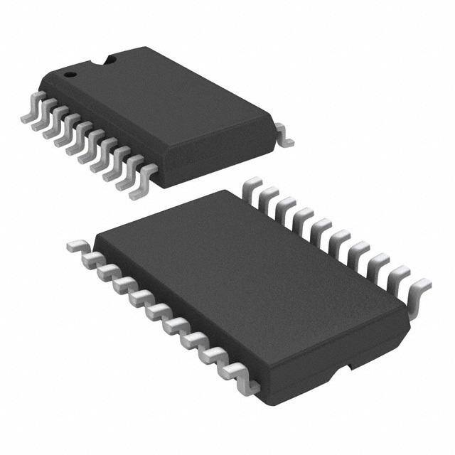
| 描述 | IC MOTOR DRIVER PAR 20SOIC马达/运动/点火控制器和驱动器 1.5A Unipol Solenoid Relay Driver |
| 产品分类 | PMIC - 电机, 电桥式驱动器集成电路 - IC |
| 品牌 | Texas Instruments |
| 产品手册 | http://www.ti.com/litv/slvsaw5b |
| 产品图片 |
|
| rohs | 符合RoHS无铅 / 符合限制有害物质指令(RoHS)规范要求 |
| 产品系列 | 电源管理 IC,马达/运动/点火控制器和驱动器,Texas Instruments DRV8803DW- |
| 数据手册 | |
| 产品型号 | DRV8803DW |
| 产品 | Stepper Motor Controllers / Drivers |
| 产品种类 | 马达/运动/点火控制器和驱动器 |
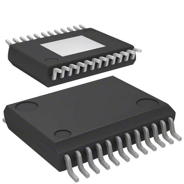
| 供应商器件封装 | 20-SOIC |
| 其它名称 | 296-29743-5 |
| 功能 | 驱动器 - 全集成,控制和功率级 |
| 包装 | 管件 |
| 商标 | Texas Instruments |
| 安装类型 | 表面贴装 |
| 安装风格 | SMD/SMT |
| 封装 | Tube |
| 封装/外壳 | 20-SOIC(0.295",7.50mm 宽) |
| 封装/箱体 | SOIC-20 |
| 工作温度 | -40°C ~ 85°C |
| 工作电源电压 | 8.2 V to 60 V |
| 工厂包装数量 | 25 |
| 应用 | 通用 |
| 接口 | 并联 |
| 标准包装 | 25 |
| 电压-电源 | 8.2 V ~ 60 V |
| 电压-负载 | 8.2 V ~ 60 V |
| 电机类型-AC,DC | 有刷直流 |
| 电机类型-步进 | 单极 |
| 电流-输出 | 1.5A |
| 电源电流 | 1.6 mA |
| 类型 | 4-Channel Protected Low-Side Driver |
| 系列 | DRV8803 |
| 输出电流 | 2 A |
| 输出端数量 | 4 Output |
| 输出配置 | 低压侧驱动器,(4) 四 |


- 商务部:美国ITC正式对集成电路等产品启动337调查
- 曝三星4nm工艺存在良率问题 高通将骁龙8 Gen1或转产台积电
- 太阳诱电将投资9.5亿元在常州建新厂生产MLCC 预计2023年完工
- 英特尔发布欧洲新工厂建设计划 深化IDM 2.0 战略
- 台积电先进制程称霸业界 有大客户加持明年业绩稳了
- 达到5530亿美元!SIA预计今年全球半导体销售额将创下新高
- 英特尔拟将自动驾驶子公司Mobileye上市 估值或超500亿美元
- 三星加码芯片和SET,合并消费电子和移动部门,撤换高东真等 CEO
- 三星电子宣布重大人事变动 还合并消费电子和移动部门
- 海关总署:前11个月进口集成电路产品价值2.52万亿元 增长14.8%


PDF Datasheet 数据手册内容提取
Product Sample & Technical Tools & Support & Folder Buy Documents Software Community DRV8803 SLVSAW5C–JULY2011–REVISEDNOVEMBER2015 DRV8803 Quad Low-Side Driver IC 1 Features 3 Description • 4-ChannelProtectedLow-SideDriver The DRV8803 provides a 4-channel low side driver 1 with overcurrent protection. It has built-in diodes to – FourNMOSFETsWithOvercurrentProtection clamp turnoff transients generated by inductive loads – IntegratedInductiveClampDiodes andcanbeusedtodriveunipolarsteppermotors,DC – ParallelInterface motors,relays,solenoids,orotherloads. • DWPackage:1.5-A(SingleChannelOn)/ In the SOIC (DW) package, the DRV8803 can supply 800-mA(FourChannelsOn)MaximumDrive up to 1.5-A (one channel on) or 800-mA (all channels CurrentperChannel(at25°C) on)continuousoutputcurrentperchannel,at25°C.In the HTSSOP (PWP) package, it can supply up to 2-A • PWPPackage:2-A(SingleChannelOn)/ (one channel on) or 1-A (four channels on) 1-A(FourChannelsOn)MaximumDriveCurrent continuous output current per channel, at 25°C with perChannel(at25°C,WithProperPCB properPCBheatsinking. Heatsinking) The device is controlled through a simple parallel • 8.2-Vto60-VOperatingSupplyVoltageRange interface. • ThermallyEnhancedSurfaceMountPackage Internal shutdown functions are provided for over 2 Applications current protection, short circuit protection, undervoltage lockout and overtemperature and faults • RelayDrivers areindicatedbyafaultoutputpin. • UnipolarStepperMotorDrivers The DRV8803 is available in a 20-pin thermally- • SolenoidDrivers enhanced SOIC package and a 16-pin HTSSOP • GeneralLow-SideSwitchApplications package(Eco-friendly:RoHS& noSb/Br). DeviceInformation(1) PARTNUMBER PACKAGE BODYSIZE(NOM) SOIC(20) 12.80mm×7.50mm DRV8803 HTSSOP(16) 5.00mm×4.40mm (1) For all available packages, see the orderable addendum at theendofthedatasheet. SimplifiedSchematic 8.2Vto60V DRV8803 5 EN /IN 1A Quad + M RESET Low-Side Controller 1A – Driver nFAULT 1A + – Fault Protection Clamp 1A Diodes 1 An IMPORTANT NOTICE at the end of this data sheet addresses availability, warranty, changes, use in safety-critical applications, intellectualpropertymattersandotherimportantdisclaimers.PRODUCTIONDATA.
DRV8803 SLVSAW5C–JULY2011–REVISEDNOVEMBER2015 www.ti.com Table of Contents 1 Features.................................................................. 1 7.4 DeviceFunctionalModes..........................................9 2 Applications........................................................... 1 8 ApplicationandImplementation........................ 10 3 Description............................................................. 1 8.1 ApplicationInformation............................................10 4 RevisionHistory..................................................... 2 8.2 TypicalApplication .................................................10 5 PinConfigurationandFunctions......................... 3 9 PowerSupplyRecommendations...................... 12 9.1 BulkCapacitance....................................................12 6 Specification........................................................... 4 10 Layout................................................................... 13 6.1 AbsoluteMaximumRatings......................................4 6.2 ESDRatings ............................................................4 10.1 LayoutGuidelines.................................................13 6.3 RecommendedOperatingConditions.......................4 10.2 LayoutExample....................................................13 6.4 ThermalInformation..................................................4 10.3 ThermalConsideration..........................................13 6.5 ElectricalCharacteristics...........................................5 11 DeviceandDocumentationSupport................. 15 6.6 TimingRequirements................................................6 11.1 DocumentationSupport........................................15 6.7 TypicalCharacteristics..............................................7 11.2 CommunityResources..........................................15 7 DetailedDescription.............................................. 8 11.3 Trademarks...........................................................15 7.1 Overview...................................................................8 11.4 ElectrostaticDischargeCaution............................15 7.2 FunctionalBlockDiagram.........................................8 11.5 Glossary................................................................15 7.3 FeatureDescription...................................................8 12 Mechanical,Packaging,andOrderable Information........................................................... 15 4 Revision History NOTE:Pagenumbersforpreviousrevisionsmaydifferfrompagenumbersinthecurrentversion. ChangesfromRevisionB(February2012)toRevisionC Page • AddedESDRatingstable,FeatureDescriptionsection,DeviceFunctionalModes,ApplicationandImplementation section,PowerSupplyRecommendationssection,Layoutsection,DeviceandDocumentationSupportsection,and Mechanical,Packaging,andOrderableInformationsection ................................................................................................. 1 • ChangedContinuousoutputcurrent,singlechannelon,T =25°C,HTSSOPpackageMAXvaluefrom1.5Ato2A.......4 A • ChangedContinuousoutputcurrent,fourchannelson,T =25°C,HTSSOPpackageMAXvaluefrom0.8Ato1A ........4 A 2 SubmitDocumentationFeedback Copyright©2011–2015,TexasInstrumentsIncorporated ProductFolderLinks:DRV8803
DRV8803 www.ti.com SLVSAW5C–JULY2011–REVISEDNOVEMBER2015 5 Pin Configuration and Functions DWPackage 20-PinSOIC PWPPackage TopView 16-PinHTSSOP TopView VM 1 20 nFAULT VM 1 16 nFAULT VCLAMP 2 19 NC VCLAMP 2 15 NC OUT1 3 18 IN1 OUT1 3 14 IN1 OUT2 4 17 IN2 OUT2 4 13 IN2 GND 5 16 GND GND 5 GND 12 GND GND 6 15 GND OUT3 6 11 IN3 GND 7 14 GND OUT4 7 10 IN4 OUT3 8 13 IN3 nENBL 8 9 RESET OUT4 9 12 IN4 nENBL 10 11 RESET PinFunctions PIN I/O(1) DESCRIPTION EXTERNALCOMPONENTS NAME SOIC HTSSOP ORCONNECTIONS POWERANDGROUND 5,6,7, 5,12, GND — Deviceground AllpinsmustbeconnectedtoGND. 14,15,16 PPAD VM 1 1 — Devicepowersupply Connecttomotorsupply(8.2V-60V). CONTROL nENBL 10 8 I Enableinput Activelowenablesoutputs–internalpulldown ActivehighresetsinternallogicandOCP– RESET 11 9 I Resetinput internalpulldown IN1 18 14 I Channel1input IN1=1drivesOUT1low–internalpulldown IN2 17 13 I Channel2input IN2=1drivesOUT2low–internalpulldown IN3 13 11 I Channel3input IN3=1drivesOUT3low–internalpulldown IN4 12 10 I Channel4input IN4=1drivesOUT4low–internalpulldown STATUS Logiclowwheninfaultcondition nFAULT 20 16 OD Fault (overtemperature,overcurrent) OUTPUT OUT1 3 3 O Output1 Connecttoload1 OUT2 4 4 O Output2 Connecttoload2 OUT3 8 6 O Output3 Connecttoload3 OUT4 9 7 O Output4 Connecttoload4 ConnecttoVMsupply,orzenerdiodetoVM VCLAMP 2 2 — Outputclampvoltage supply (1) Directions:I=input,O=output,OD=open-drainoutput Copyright©2011–2015,TexasInstrumentsIncorporated SubmitDocumentationFeedback 3 ProductFolderLinks:DRV8803
DRV8803 SLVSAW5C–JULY2011–REVISEDNOVEMBER2015 www.ti.com 6 Specification 6.1 Absolute Maximum Ratings overoperatingfree-airtemperaturerange(unlessotherwisenoted) (1) MIN MAX UNIT VM Powersupplyvoltage –0.3 65 V VOUTx Outputvoltage –0.3 65 V VCLAMP Clampvoltage –0.3 65 V nFAULT Outputcurrent 20 mA Peakclampdiodecurrent 2 A DCorRMSclampdiodecurrent 1 A Digitalinputpinvoltage –0.5 7 V nFAULT Digitaloutputpinvoltage –0.5 7 V Peakmotordriveoutputcurrent,t<1μS Internallylimited A Continuoustotalpowerdissipation SeeThermalInformation T Operatingvirtualjunctiontemperature –40 150 °C J T Storagetemperature –60 150 °C stg (1) StressesbeyondthoselistedunderAbsoluteMaximumRatingsmaycausepermanentdamagetothedevice.Thesearestressratings only,whichdonotimplyfunctionaloperationofthedeviceattheseoranyotherconditionsbeyondthoseindicatedunderRecommended OperatingConditions.Exposuretoabsolute-maximum-ratedconditionsforextendedperiodsmayaffectdevicereliability. 6.2 ESD Ratings VALUE UNIT Electrostatic Humanbodymodel(HBM),perANSI/ESDA/JEDECJS-001,allpins(1) ±3000 V V (ESD) discharge Chargeddevicemodel(CDM),perJEDECspecificationJESD22-C101,allpins(2) ±1000 (1) JEDECdocumentJEP155statesthat500-VHBMallowssafemanufacturingwithastandardESDcontrolprocess. (2) JEDECdocumentJEP157statesthat250-VCDMallowssafemanufacturingwithastandardESDcontrolprocess. 6.3 Recommended Operating Conditions MIN NOM MAX UNIT V Powersupplyvoltage 8.2 60 V M V Outputclampvoltage(1) 0 60 V CLAMP Singlechannelon 1.5 SOICpackage(2),T =25°C A Fourchannelson 0.8 I Continuousoutputcurrent A OUT Singlechannelon 2 HTSSOPpackage(2),T =25°C A Fourchannelson 1 (1) V isusedonlytosupplytheclampdiodes.Itisnotapowersupplyinput. CLAMP (2) Powerdissipationandthermallimitsmustbeobserved. 6.4 Thermal Information DRV8803 THERMALMETRIC(1) DW(SOIC) PWP(HTSSOP) UNIT 20PINS 16PINS R Junction-to-ambientthermalresistance 67.7 39.6 °C/W θJA R Junction-to-case(top)thermalresistance 32.9 24.6 °C/W θJC(top) R Junction-to-boardthermalresistance 35.4 20.3 °C/W θJB ψ Junction-to-topcharacterizationparameter 8.2 0.7 °C/W JT ψ Junction-to-boardcharacterizationparameter 34.9 20.1 °C/W JB R Junction-to-case(bottom)thermalresistance N/A 2.3 °C/W θJC(bot) (1) Formoreinformationabouttraditionalandnewthermalmetrics,seetheSemiconductorandICPackageThermalMetricsapplication report,SPRA953. 4 SubmitDocumentationFeedback Copyright©2011–2015,TexasInstrumentsIncorporated ProductFolderLinks:DRV8803
DRV8803 www.ti.com SLVSAW5C–JULY2011–REVISEDNOVEMBER2015 6.5 Electrical Characteristics T =25°C,overrecommendedoperatingconditions(unlessotherwisenoted) A PARAMETER TESTCONDITIONS MIN TYP MAX UNIT POWERSUPPLIES I VMoperatingsupplycurrent V =24V 1.6 2.1 mA VM M VMundervoltagelockout V V rising 8.2 V UVLO voltage M LOGIC-LEVELINPUTS(SCHMITTTRIGGERINPUTSWITHHYSTERESIS) V Inputlowvoltage 0.6 0.7 V IL V Inputhighvoltage 2 V IH V Inputhysteresis 0.45 V HYS I Inputlowcurrent VIN=0 –20 20 μA IL I Inputhighcurrent VIN=3.3V 100 μA IH R Pulldownresistance 100 kΩ PD nFAULTOUTPUT(OPEN-DRAINOUTPUT) V Outputlowvoltage I =5mA 0.5 V OL O I Outputhighleakagecurrent V =3.3V 1 μA OH O LOW-SIDEFETS V =24V,I =700mA,T =25°C 0.5 M O J R FETonresistance Ω DS(ON) V =24V,I =700mA,T =85°C 0.75 0.8 M O J I Off-stateleakagecurrent –50 50 μA OFF HIGH-SIDEDIODES V Diodeforwardvoltage V =24V,I =700mA,T =25°C 1.2 V F M O J I Off-stateleakagecurrent V =24V,T =25°C –50 50 μA OFF M J OUTPUTS t Risetime V =24V,I =700mA,Resistiveload 50 300 ns R M O t Falltime V =24V,I =700mA,Resistiveload 50 300 ns F M O PROTECTIONCIRCUITS I Overcurrentprotectiontriplevel 2.3 3.8 A OCP Overcurrentprotectiondeglitch t 3.5 µs OCP time Overcurrentprotectionretry t 1.2 ms RETRY time t Thermalshutdowntemperature Dietemperature(1) 150 160 180 °C TSD (1) Notproductiontested. Copyright©2011–2015,TexasInstrumentsIncorporated SubmitDocumentationFeedback 5 ProductFolderLinks:DRV8803
DRV8803 SLVSAW5C–JULY2011–REVISEDNOVEMBER2015 www.ti.com 6.6 Timing Requirements overoperatingfree-airtemperaturerange(unlessotherwisenoted)(1) MIN MAX UNIT 1 t Enabletime,nENBLtooutputlow 50 ns OE(ENABLE) 2 t Propagationdelaytime,INxtoOUTx,lowtohigh 800 ns PD(L-H) 3 t Propagationdelaytime,INxtoOUTx,hightolow 800 ns PD(H-L) — t RESETpulsewidth 20 µs RESET (1) Notproductiontested. nENBL INx OUTx 1 2 3 Figure1. DRV8803TimingRequirements 6 SubmitDocumentationFeedback Copyright©2011–2015,TexasInstrumentsIncorporated ProductFolderLinks:DRV8803
DRV8803 www.ti.com SLVSAW5C–JULY2011–REVISEDNOVEMBER2015 6.7 Typical Characteristics 1.80 1.80 1.75 1.75 1.70 1.70 mA) 1.65 mA) 1.65 Current (11..5650 Current (11..5650 Supply 11..4550 Supply 11..4550 1.40 8 V 24 V 1.40 -40° C 25° C 1.35 1.35 30 V 60 V 75° C 125° C 1.30 1.30 -40° C 25° C 75° C 125° C 8 V 24 V 30 V 60 V Temperature ((cid:131)C) C001 Supply Voltage (V) C002 Figure2.SupplyCurrentOverTemperature Figure3.SupplyCurrentOverVM 900 1000 -40° C 25° C 900 75° C 125° C 800 800 700 (cid:159)) (cid:159)) 700 m m n (600 n ( 600 o o s s Rd Rd 500 500 400 400 8 V 300 60 V 300 200 -40° C 25° C 75° C 125° C 8 V 60 V Temperature ((cid:131)C) Supply Voltage (V) C005 C006 Figure4.R OverTemperature Figure5.R OverV DS(on) DS(on) M Copyright©2011–2015,TexasInstrumentsIncorporated SubmitDocumentationFeedback 7 ProductFolderLinks:DRV8803
DRV8803 SLVSAW5C–JULY2011–REVISEDNOVEMBER2015 www.ti.com 7 Detailed Description 7.1 Overview The DRV8803 device is an integrated 4-channel low side driver solution for any low side switch application. The integrated overcurrent protection limits the motor current to a fixed maximum. Four logic inputs control the low- side driver outputs which consist of four N-channel MOSFETs that have a typical R of 500 mΩ. A single DS(on) power input VM serves as device power and is internally regulated to power the internal low side gate drive. Motor speed can be controlled with pulse-width modulation at frequencies from 0 kHz to 100 kHz. The device outputs can be disabled by bringing nENBL pin high. The thermal shutdown protection enables the device to automatically shut down if the die temperature exceeds a TTSD limit. UVLO protection will disable all circuitry in thedeviceifV dropsbelowtheundervoltagelockoutthreshold. M 7.2 Functional Block Diagram 8.2V–60V 8.2V–60V Internal Int.VCC Optional VM Reference Zener LS Gate Regs Drive UVLO VCLAMP nENBL OCP OUT1 & Inductive RESET Gate Load Drive IN1 OUT2 OCP IN2 & Inductive Gate Load Drive IN3 Control Logic IN4 OCP OUT3 & Inductive Gate Load Drive nFAULT OCP OUT4 Thermal & Inductive Shut down Gate Load Drive GND (multiple pins) 7.3 Feature Description 7.3.1 OutputDrivers The DRV8803 device contains four protected low-side drivers. Each output has an integrated clamp diode connectedtoacommonpin,VCLAMP. VCLAMP can be connected to the main power supply voltage, VM. VCLAMP can also be connected to a Zener or TVS diode to VM, allowing the switch voltage to exceed the main supply voltage VM. This connection can be beneficialwhendrivingloadsthatrequireveryfastcurrentdecay,suchasunipolarsteppermotors. Inallcases,thevoltageontheoutputsmustnotbeallowedtoexceedthemaximumoutputvoltagespecification. 8 SubmitDocumentationFeedback Copyright©2011–2015,TexasInstrumentsIncorporated ProductFolderLinks:DRV8803
DRV8803 www.ti.com SLVSAW5C–JULY2011–REVISEDNOVEMBER2015 Feature Description (continued) 7.3.2 ProtectionCircuits TheDRV8803deviceisfullyprotectedagainstundervoltage,overcurrentandovertemperatureevents. 7.3.2.1 OvercurrentProtection(OCP) An analog current limit circuit on each FET limits the current through the FET by removing the gate drive. If this analog current limit persists for longer than the t deglitch time (approximately 3.5 µs), the driver will be OCP disabled and the nFAULT pin will be driven low. The driver will remain disabled for the t retry time RETRY (approximately 1.2 ms), then the fault will be automatically cleared. The fault will be cleared immediately if either RESETpinisactivatedorVMisremovedandreapplied. 7.3.2.2 ThermalShutdown(TSD) Ifthedietemperatureexceedssafelimits,alloutputFETswillbedisabledandthenFAULTpinwillbedrivenlow. Oncethedietemperaturehasfallentoasafelevel,operationwillautomaticallyresume. 7.3.2.3 UndervoltageLockout(UVLO) If at any time the voltage on the VM pin falls below the undervoltage lockout threshold voltage, all circuitry in the device will be disabled, and internal logic will be reset. Operation will resume when VM rises above the UVLO threshold. 7.4 Device Functional Modes 7.4.1 ParallelInterfaceOperation TheDRV8803deviceiscontrolledwithasimpleparallelinterface.Logically,theinterfaceisshowninFigure6. nENBL OUT1 IN1 OUT2 IN2 OUT3 IN3 OUT4 IN4 Figure6. ParallelInterfaceOperation 7.4.2 nENBLandRESETOperation The nENBL pin enables or disables the output drivers. nENBL must be low to enable the outputs. Note that nENBLhasaninternalpulldown. The RESET pin, when driven active high, resets internal logic. All inputs are ignored while RESET is active. Note that RESET has an internal pulldown. An internal power-up reset is also provided, so it is not required to drive RESETatpowerup. Copyright©2011–2015,TexasInstrumentsIncorporated SubmitDocumentationFeedback 9 ProductFolderLinks:DRV8803
DRV8803 SLVSAW5C–JULY2011–REVISEDNOVEMBER2015 www.ti.com 8 Application and Implementation NOTE Information in the following applications sections is not part of the TI component specification, and TI does not warrant its accuracy or completeness. TI’s customers are responsible for determining suitability of components for their purposes. Customers should validateandtesttheirdesignimplementationtoconfirmsystemfunctionality. 8.1 Application Information TheDRV8803devicecanbeusedtodriveoneunipolarsteppermotor. 8.2 Typical Application VM + 0.1 µF 100µF 1 20 VM nFAULT 2 19 VCLAMP NC 3 18 M – OUT1 IN1 4 17 + OUT2 IN2 5 16 GND GND + – 6 DRV8803 15 GND GND 7 14 GND GND 8 13 OUT3 IN3 9 12 OUT4 IN4 10 11 nENBL RESET Figure7. TypicalApplicationSchematic 8.2.1 DesignRequirements Table1liststhedesignparametersforthisdesignexample. Table1.DesignParameters DESIGNPARAMETER REFERENCE EXAMPLEVALUE SupplyVoltage V 24V M MotorWindingResistance R 7.4Ω/phase L MotorFullStepAngle θ 1.8°/step step MotorRatedCurrent I 0.75A RATED PWMfrequency f 31.25kHz PWM 8.2.2 DetailedDesignProcedure 8.2.2.1 MotorVoltage The motor voltage to use will depend on the ratings of the motor selected and the desired torque. A higher voltage shortens the current rise time in the coils of the stepper motor allowing the motor to produce a greater averagetorque.Usingahighervoltagealsoallowsthemotortooperateatafasterspeedthanalowervoltage. 8.2.2.2 DriveCurrent The current path is starts from the supply VM, moves through the inductive winding load, and low-side sinking NMOSpowerFET.PowerdissipationlossesinonesinkNMOSpowerFETareshowninEquation1. P=I2×R (1) DS(on) 10 SubmitDocumentationFeedback Copyright©2011–2015,TexasInstrumentsIncorporated ProductFolderLinks:DRV8803
DRV8803 www.ti.com SLVSAW5C–JULY2011–REVISEDNOVEMBER2015 The DRV8803 device has been measured to be capable of 1.5-A Single Channel or 800-mA Four Channels with the DW package and 2-A Single Channel or 1-A Four Channels with the PWP package at 25°C on standard FR- 4PCBs.ThemaximumRMScurrentvariesbasedonPCBdesignandtheambienttemperature. 8.2.3 ApplicationCurves Figure8.CurrentRampWitha16-Ω,1-mHRLLoadandV Figure9.CurrentRampWitha16-Ω,1-mHRLLoadandV M M =8.2V =30V Figure10.OCPWithV =8.2VandOUT1ShortedtoV Figure11.OCPSeparatedbyt WithV =8.2-Vand M M RETRY M OUT1ShortedtoV M Copyright©2011–2015,TexasInstrumentsIncorporated SubmitDocumentationFeedback 11 ProductFolderLinks:DRV8803
DRV8803 SLVSAW5C–JULY2011–REVISEDNOVEMBER2015 www.ti.com 9 Power Supply Recommendations 9.1 Bulk Capacitance Having appropriate local bulk capacitance is an important factor in motor drive system design. It is generally beneficialtohavemorebulkcapacitance,whilethedisadvantagesareincreasedcostandphysicalsize. Theamountoflocalcapacitanceneededdependsonavarietyoffactors,including: • Thehighestcurrentrequiredbythemotorsystem. • Thepowersupply’scapacitanceandabilitytosourcecurrent. • Theamountofparasiticinductancebetweenthepowersupplyandmotorsystem. • Theacceptablevoltageripple. • Thetypeofmotorused(BrushedDC,BrushlessDC,Stepper). • Themotorbrakingmethod. The inductance between the power supply and motor drive system will limit the rate current can change from the power supply. If the local bulk capacitance is too small, the system will respond to excessive current demands or dumps from the motor with a change in voltage. When adequate bulk capacitance is used, the motor voltage remainsstableandhighcurrentcanbequicklysupplied. The inductance between the power supply and motor drive system will limit the rate current can change from the power supply. If the local bulk capacitance is too small, the system will respond to excessive current demands or dumps from the motor with a change in voltage. When adequate bulk capacitance is used, the motor voltage remainsstableandhighcurrentcanbequicklysupplied. Parasitic Wire Inductance Power Supply Motor Drive System VM + + Motor – Driver GND Local IC Bypass Bulk Capacitor Capacitor ExampleSetupofMotorDriveSystemwithExternalPowerSupply Figure12. ExampleSetupofMotorDriveSystemWithExternalPowerSupply The voltage rating for bulk capacitors should be higher than the operating voltage, to provide margin for cases whenthemotortransfersenergytothesupply. 12 SubmitDocumentationFeedback Copyright©2011–2015,TexasInstrumentsIncorporated ProductFolderLinks:DRV8803
DRV8803 www.ti.com SLVSAW5C–JULY2011–REVISEDNOVEMBER2015 10 Layout 10.1 Layout Guidelines The bulk capacitor should be placed to minimize the distance of the high-current path through the motor driver device. The connecting metal trace widths should be as wide as possible, and numerous vias should be used when connecting PCB layers. These practices minimize inductance and allow the bulk capacitor to deliver high current. Small-valuecapacitorsshouldbeceramic,andplacedcloselytodevicepins. Thehigh-currentdeviceoutputsshouldusewidemetaltraces. The device thermal pad should be soldered to the PCB top-layer ground plane. Multiple vias should be used to connect to a large bottom-layer ground plane. The use of large metal planes and multiple vias help dissipate the I2×R heatthatisgeneratedinthedevice. DS(on) 10.2 Layout Example + VM nFAULT VCLAMP NC OUT1 IN1 OUT2 IN2 GND GND OUT3 IN3 OUT4 IN4 nENBL RESET Figure13. RecommendedLayout 10.3 Thermal Consideration 10.3.1 ThermalProtection The DRV8803 device has thermal shutdown (TSD) as described above. If the die temperature exceeds approximately150°C,thedevicewillbedisableduntilthetemperaturedropstoasafelevel. Any tendency of the device to enter TSD is an indication of either excessive power dissipation, insufficient heatsinking,ortoohighanambienttemperature. 10.3.2 PowerDissipation Power dissipation in the DRV8803 device is dominated by the power dissipated in the output FET resistance, or R . Average power dissipation of each FET when running a static load can be roughly estimated by DS(on) Equation2: P= R ·(I )2 DS(ON) OUT where • PisthepowerdissipationofoneFET Copyright©2011–2015,TexasInstrumentsIncorporated SubmitDocumentationFeedback 13 ProductFolderLinks:DRV8803
DRV8803 SLVSAW5C–JULY2011–REVISEDNOVEMBER2015 www.ti.com Thermal Consideration (continued) • R istheresistanceofeachFET DS(ON) • I isequaltotheaveragecurrentdrawnbytheload. (2) OUT At start-up and fault conditions, this current is much higher than normal running current; consider these peak currents and their duration. When driving more than one load simultaneously, the power in all active output stagesmustbesummed. The maximum amount of power that can be dissipated in the device is dependent on ambient temperature and heatsinking. Note that R increases with temperature, so as the device heats, the power dissipation increases. This must DS(on) betakenintoconsiderationwhensizingtheheatsink. 10.3.3 Heatsinking The DRV8803DW package uses a standard SOIC outline, but has the center pins internally fused to the die pad to more efficiently remove heat from the device. The two center leads on each side of the package should be connected together to as large a copper area on the PCB as is possible to remove heat from the device. If the copper area is on the opposite side of the PCB from the device, thermal vias are used to transfer the heat betweentopandbottomlayers. Ingeneral,themorecopperareathatcanbeprovided,themorepowercanbedissipated. TheDRV8803PWPpackageusesanHTSSOPpackagewithanexposed PowerPAD™.ThePowerPADpackage uses an exposed pad to remove heat from the device. For proper operation, this pad must be thermally connected to copper on the PCB to dissipate heat. On a multi-layer PCB with a ground plane, this can be accomplished by adding a number of vias to connect the thermal pad to the ground plane. On PCBs without internal planes, copper area can be added on either side of the PCB to dissipate heat. If the copper area is on the opposite side of the PCB from the device, thermal vias are used to transfer the heat between top and bottom layers. For details about how to design the PCB, see the TI Application Report, PowerPAD Thermally Enhanced Package(SLMA002),andTIApplicationBrief, PowerPADMadeEasy(SLMA004),availableatwww.ti.com. 14 SubmitDocumentationFeedback Copyright©2011–2015,TexasInstrumentsIncorporated ProductFolderLinks:DRV8803
DRV8803 www.ti.com SLVSAW5C–JULY2011–REVISEDNOVEMBER2015 11 Device and Documentation Support 11.1 Documentation Support 11.1.1 RelatedDocumentation Forrelateddocumentationseethefollowing: • PowerPADThermallyEnhancedPackage,SLMA002. • PowerPADMadeEasy,SLMA004. 11.2 Community Resources The following links connect to TI community resources. Linked contents are provided "AS IS" by the respective contributors. They do not constitute TI specifications and do not necessarily reflect TI's views; see TI's Terms of Use. TIE2E™OnlineCommunity TI'sEngineer-to-Engineer(E2E)Community.Createdtofostercollaboration amongengineers.Ate2e.ti.com,youcanaskquestions,shareknowledge,exploreideasandhelp solveproblemswithfellowengineers. DesignSupport TI'sDesignSupport QuicklyfindhelpfulE2Eforumsalongwithdesignsupporttoolsand contactinformationfortechnicalsupport. 11.3 Trademarks PowerPAD,E2EaretrademarksofTexasInstruments. Allothertrademarksarethepropertyoftheirrespectiveowners. 11.4 Electrostatic Discharge Caution Thesedeviceshavelimitedbuilt-inESDprotection.Theleadsshouldbeshortedtogetherorthedeviceplacedinconductivefoam duringstorageorhandlingtopreventelectrostaticdamagetotheMOSgates. 11.5 Glossary SLYZ022—TIGlossary. Thisglossarylistsandexplainsterms,acronyms,anddefinitions. 12 Mechanical, Packaging, and Orderable Information The following pages include mechanical, packaging, and orderable information. This information is the most current data available for the designated devices. This data is subject to change without notice and revision of thisdocument.Forbrowser-basedversionsofthisdatasheet,refertotheleft-handnavigation. Copyright©2011–2015,TexasInstrumentsIncorporated SubmitDocumentationFeedback 15 ProductFolderLinks:DRV8803
PACKAGE OPTION ADDENDUM www.ti.com 6-Feb-2020 PACKAGING INFORMATION Orderable Device Status Package Type Package Pins Package Eco Plan Lead/Ball Finish MSL Peak Temp Op Temp (°C) Device Marking Samples (1) Drawing Qty (2) (6) (3) (4/5) DRV8803DW ACTIVE SOIC DW 20 25 Green (RoHS NIPDAU Level-2-260C-1 YEAR -40 to 125 DRV8803DW & no Sb/Br) DRV8803DWR ACTIVE SOIC DW 20 2000 Green (RoHS NIPDAU Level-2-260C-1 YEAR -40 to 125 DRV8803DW & no Sb/Br) DRV8803PWP ACTIVE HTSSOP PWP 16 90 Green (RoHS NIPDAU Level-3-260C-168 HR -40 to 125 DRV8803 & no Sb/Br) DRV8803PWPR ACTIVE HTSSOP PWP 16 2000 Green (RoHS NIPDAU Level-3-260C-168 HR -40 to 125 DRV8803 & no Sb/Br) (1) The marketing status values are defined as follows: ACTIVE: Product device recommended for new designs. LIFEBUY: TI has announced that the device will be discontinued, and a lifetime-buy period is in effect. NRND: Not recommended for new designs. Device is in production to support existing customers, but TI does not recommend using this part in a new design. PREVIEW: Device has been announced but is not in production. Samples may or may not be available. OBSOLETE: TI has discontinued the production of the device. (2) RoHS: TI defines "RoHS" to mean semiconductor products that are compliant with the current EU RoHS requirements for all 10 RoHS substances, including the requirement that RoHS substance do not exceed 0.1% by weight in homogeneous materials. Where designed to be soldered at high temperatures, "RoHS" products are suitable for use in specified lead-free processes. TI may reference these types of products as "Pb-Free". RoHS Exempt: TI defines "RoHS Exempt" to mean products that contain lead but are compliant with EU RoHS pursuant to a specific EU RoHS exemption. Green: TI defines "Green" to mean the content of Chlorine (Cl) and Bromine (Br) based flame retardants meet JS709B low halogen requirements of <=1000ppm threshold. Antimony trioxide based flame retardants must also meet the <=1000ppm threshold requirement. (3) MSL, Peak Temp. - The Moisture Sensitivity Level rating according to the JEDEC industry standard classifications, and peak solder temperature. (4) There may be additional marking, which relates to the logo, the lot trace code information, or the environmental category on the device. (5) Multiple Device Markings will be inside parentheses. Only one Device Marking contained in parentheses and separated by a "~" will appear on a device. If a line is indented then it is a continuation of the previous line and the two combined represent the entire Device Marking for that device. (6) Lead/Ball Finish - Orderable Devices may have multiple material finish options. Finish options are separated by a vertical ruled line. Lead/Ball Finish values may wrap to two lines if the finish value exceeds the maximum column width. Important Information and Disclaimer:The information provided on this page represents TI's knowledge and belief as of the date that it is provided. TI bases its knowledge and belief on information provided by third parties, and makes no representation or warranty as to the accuracy of such information. Efforts are underway to better integrate information from third parties. TI has taken and Addendum-Page 1
PACKAGE OPTION ADDENDUM www.ti.com 6-Feb-2020 continues to take reasonable steps to provide representative and accurate information but may not have conducted destructive testing or chemical analysis on incoming materials and chemicals. TI and TI suppliers consider certain information to be proprietary, and thus CAS numbers and other limited information may not be available for release. In no event shall TI's liability arising out of such information exceed the total purchase price of the TI part(s) at issue in this document sold by TI to Customer on an annual basis. Addendum-Page 2
PACKAGE MATERIALS INFORMATION www.ti.com 26-Feb-2019 TAPE AND REEL INFORMATION *Alldimensionsarenominal Device Package Package Pins SPQ Reel Reel A0 B0 K0 P1 W Pin1 Type Drawing Diameter Width (mm) (mm) (mm) (mm) (mm) Quadrant (mm) W1(mm) DRV8803DWR SOIC DW 20 2000 330.0 24.4 10.8 13.3 2.7 12.0 24.0 Q1 DRV8803PWPR HTSSOP PWP 16 2000 330.0 12.4 6.9 5.6 1.6 8.0 12.0 Q1 PackMaterials-Page1
PACKAGE MATERIALS INFORMATION www.ti.com 26-Feb-2019 *Alldimensionsarenominal Device PackageType PackageDrawing Pins SPQ Length(mm) Width(mm) Height(mm) DRV8803DWR SOIC DW 20 2000 367.0 367.0 45.0 DRV8803PWPR HTSSOP PWP 16 2000 350.0 350.0 43.0 PackMaterials-Page2
None
PACKAGE OUTLINE PWP0016J PowerPAD TM TSSOP - 1.2 mm max height SCALE 2.500 SMALL OUTLINE PACKAGE 6.6 C SEATING TYP 6.2 PLANE A PIN 1 INDEX 0.1 C AREA 14X 0.65 16 1 2X 5.1 4.55 4.9 NOTE 3 8 9 0.30 4.5 16X B 0.19 4.3 0.1 C A B (0.15) TYP SEE DETAIL A 8 9 0.25 3.55 GAGE PLANE 1.2 MAX 2.68 0.75 0.15 0 -8 0.50 0.05 1 16 DETA 20AIL A TYPICAL 2.46 THERMAL 1.75 PAD 4223595/A 03/2017 PowerPAD is a trademark of Texas Instruments. NOTES: 1. All linear dimensions are in millimeters. Any dimensions in parenthesis are for reference only. Dimensioning and tolerancing per ASME Y14.5M. 2. This drawing is subject to change without notice. 3. This dimension does not include mold flash, protrusions, or gate burrs. Mold flash, protrusions, or gate burrs shall not exceed 0.15 mm per side. 4. Reference JEDEC registration MO-153. www.ti.com
EXAMPLE BOARD LAYOUT PWP0016J PowerPAD TM TSSOP - 1.2 mm max height SMALL OUTLINE PACKAGE (3.4) NOTE 8 METAL COVERED (2.46) BY SOLDER MASK 16X (1.5) SYMM SEE DETAILS 16X (0.45) 1 16 (1.3) TYP (R0.05) TYP SYMM (0.65) (3.55) (5) NOTE 8 14X (0.65) ( 0.2) TYP VIA 8 9 (1.35) TYP SOLDER MASK DEFINED PAD (5.8) LAND PATTERN EXAMPLE EXPOSED METAL SHOWN SCALE: 10X SOLDER MASK METAL METAL UNDER SOLDER MASK OPENING SOLDER MASK OPENING EXPOSED METAL EXPOSED METAL 0.05 MAX 0.05 MIN ALL AROUND ALL AROUND NON-SOLDER MASK SOLDER MASK DEFINED DEFINED SOLDE15.000R MASK DETAILS 4223595/A 03/2017 NOTES: (continued) 5. Publication IPC-7351 may have alternate designs. 6. Solder mask tolerances between and around signal pads can vary based on board fabrication site. 7. This package is designed to be soldered to a thermal pad on the board. For more information, see Texas Instruments literature numbers SLMA002 (www.ti.com/lit/slma002) and SLMA004 (www.ti.com/lit/slma004). 8. Size of metal pad may vary due to creepage requirement. 9. Vias are optional depending on application, refer to device data sheet. It is recommended that vias under paste be filled, plugged or tented. www.ti.com
EXAMPLE STENCIL DESIGN PWP0016J PowerPAD TM TSSOP - 1.2 mm max height SMALL OUTLINE PACKAGE (2.46) 16X (1.5) BASED ON METAL COVERED 0.125 THICK BY SOLDER MASK STENCIL 16X (0.45) 1 16 (R0.05) TYP (3.55) SYMM BASED ON 0.125 THICK STENCIL 14X (0.65) 8 9 SYMM SEE TABLE FOR DIFFERENT OPENINGS FOR OTHER STENCIL (5.8) THICKNESSES SOLDER PASTE EXAMPLE BASED ON 0.125 mm THICK STENCIL SCALE: 10X STENCIL SOLDER STENCIL THICKNESS OPENING 0.1 2.75 X 3.97 0.125 2.46 X 3.55 (SHOWN) 0.15 2.25 X 3.24 0.175 2.08 X 3.00 4223595/A 03/2017 NOTES: (continued) 10. Laser cutting apertures with trapezoidal walls and rounded corners may offer better paste release. IPC-7525 may have alternate design recommendations. 11. Board assembly site may have different recommendations for stencil design. www.ti.com
PACKAGE OUTLINE DW0020A SOIC - 2.65 mm max height SCALE 1.200 SOIC C 10.63 SEATING PLANE TYP 9.97 A PIN 1 ID 0.1 C AREA 18X 1.27 20 1 13.0 2X 12.6 11.43 NOTE 3 10 11 0.51 20X 7.6 0.31 2.65 MAX B 7.4 0.25 C A B NOTE 4 0.33 TYP 0.10 0.25 SEE DETAIL A GAGE PLANE 0.3 1.27 0 - 8 0.1 0.40 DETAIL A TYPICAL 4220724/A 05/2016 NOTES: 1. All linear dimensions are in millimeters. Dimensions in parenthesis are for reference only. Dimensioning and tolerancing per ASME Y14.5M. 2. This drawing is subject to change without notice. 3. This dimension does not include mold flash, protrusions, or gate burrs. Mold flash, protrusions, or gate burrs shall not exceed 0.15 mm per side. 4. This dimension does not include interlead flash. Interlead flash shall not exceed 0.43 mm per side. 5. Reference JEDEC registration MS-013. www.ti.com
EXAMPLE BOARD LAYOUT DW0020A SOIC - 2.65 mm max height SOIC 20X (2) SYMM 1 20 20X (0.6) 18X (1.27) SYMM (R0.05) TYP 10 11 (9.3) LAND PATTERN EXAMPLE SCALE:6X SOOPLEDNEINRG MASK METAL MSOELTDAEL RU NMDAESRK SOOPLEDNEINRG MASK 0.07 MAX 0.07 MIN ALL AROUND ALL AROUND NON SOLDER MASK SOLDER MASK DEFINED DEFINED SOLDER MASK DETAILS 4220724/A 05/2016 NOTES: (continued) 6. Publication IPC-7351 may have alternate designs. 7. Solder mask tolerances between and around signal pads can vary based on board fabrication site. www.ti.com
EXAMPLE STENCIL DESIGN DW0020A SOIC - 2.65 mm max height SOIC 20X (2) SYMM 1 20 20X (0.6) 18X (1.27) SYMM 10 11 (9.3) SOLDER PASTE EXAMPLE BASED ON 0.125 mm THICK STENCIL SCALE:6X 4220724/A 05/2016 NOTES: (continued) 8. Laser cutting apertures with trapezoidal walls and rounded corners may offer better paste release. IPC-7525 may have alternate design recommendations. 9. Board assembly site may have different recommendations for stencil design. www.ti.com
IMPORTANTNOTICEANDDISCLAIMER TI PROVIDES TECHNICAL AND RELIABILITY DATA (INCLUDING DATASHEETS), DESIGN RESOURCES (INCLUDING REFERENCE DESIGNS), APPLICATION OR OTHER DESIGN ADVICE, WEB TOOLS, SAFETY INFORMATION, AND OTHER RESOURCES “AS IS” AND WITH ALL FAULTS, AND DISCLAIMS ALL WARRANTIES, EXPRESS AND IMPLIED, INCLUDING WITHOUT LIMITATION ANY IMPLIED WARRANTIES OF MERCHANTABILITY, FITNESS FOR A PARTICULAR PURPOSE OR NON-INFRINGEMENT OF THIRD PARTY INTELLECTUAL PROPERTY RIGHTS. These resources are intended for skilled developers designing with TI products. You are solely responsible for (1) selecting the appropriate TI products for your application, (2) designing, validating and testing your application, and (3) ensuring your application meets applicable standards, and any other safety, security, or other requirements. These resources are subject to change without notice. TI grants you permission to use these resources only for development of an application that uses the TI products described in the resource. Other reproduction and display of these resources is prohibited. No license is granted to any other TI intellectual property right or to any third party intellectual property right. TI disclaims responsibility for, and you will fully indemnify TI and its representatives against, any claims, damages, costs, losses, and liabilities arising out of your use of these resources. TI’s products are provided subject to TI’s Terms of Sale (www.ti.com/legal/termsofsale.html) or other applicable terms available either on ti.com or provided in conjunction with such TI products. TI’s provision of these resources does not expand or otherwise alter TI’s applicable warranties or warranty disclaimers for TI products. Mailing Address: Texas Instruments, Post Office Box 655303, Dallas, Texas 75265 Copyright © 2020, Texas Instruments Incorporated