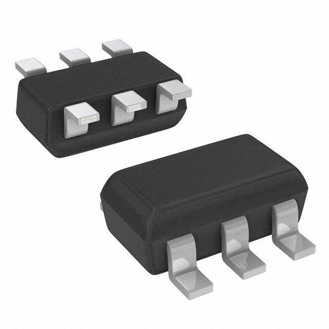
ICGOO在线商城 > DRV590DWP
- 型号: DRV590DWP
- 制造商: Texas Instruments
- 库位|库存: xxxx|xxxx
- 要求:
| 数量阶梯 | 香港交货 | 国内含税 |
| +xxxx | $xxxx | ¥xxxx |
查看当月历史价格
查看今年历史价格
DRV590DWP产品简介:
ICGOO电子元器件商城为您提供DRV590DWP由Texas Instruments设计生产,在icgoo商城现货销售,并且可以通过原厂、代理商等渠道进行代购。 提供DRV590DWP价格参考以及Texas InstrumentsDRV590DWP封装/规格参数等产品信息。 你可以下载DRV590DWP参考资料、Datasheet数据手册功能说明书, 资料中有DRV590DWP详细功能的应用电路图电压和使用方法及教程。
| 参数 | 数值 |
| 产品目录 | 集成电路 (IC)半导体 |
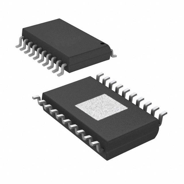
| 描述 | IC PWM POWER DRVR HI-EFF 20SOPWR门驱动器 High Efficiency PWM Power Driver |
| 产品分类 | |
| 品牌 | Texas Instruments |
| 产品手册 | |
| 产品图片 |
|
| rohs | 符合RoHS无铅 / 符合限制有害物质指令(RoHS)规范要求 |
| 产品系列 | 电源管理 IC,门驱动器,Texas Instruments DRV590DWP- |
| 数据手册 | |
| 产品型号 | DRV590DWP |
| 产品 | Driver ICs - Various |
| 产品目录页面 | |
| 产品种类 | 门驱动器 |
| 供应商器件封装 | 20-SO PowerPad |
| 其它名称 | 296-12201-5 |
| 包装 | 管件 |
| 单位重量 | 506.600 mg |
| 商标 | Texas Instruments |
| 安装类型 | 表面贴装 |
| 安装风格 | SMD/SMT |
| 封装 | Tube |
| 封装/外壳 | 20-SOIC(0.295",7.50mm 宽)裸露焊盘 |
| 封装/箱体 | HSOP-20 |
| 工作温度 | -40°C ~ 85°C |
| 工厂包装数量 | 25 |
| 应用 | 热电冷却器 |
| 最大功率耗散 | 3.6 W |
| 最大工作温度 | + 85 C |
| 最小工作温度 | - 40 C |
| 标准包装 | 25 |
| 激励器数量 | 1 Driver |
| 电压-电源 | 2.7 V ~ 5.5 V |
| 电流-电源 | 4.5mA |
| 电源电压-最大 | 5.5 V |
| 电源电压-最小 | 2.7 V |
| 电源电流 | 6.5 mA |
| 类型 | Non-Inverting |
| 系列 | DRV590 |
| 输出电流 | 1.22 A |




- 商务部:美国ITC正式对集成电路等产品启动337调查
- 曝三星4nm工艺存在良率问题 高通将骁龙8 Gen1或转产台积电
- 太阳诱电将投资9.5亿元在常州建新厂生产MLCC 预计2023年完工
- 英特尔发布欧洲新工厂建设计划 深化IDM 2.0 战略
- 台积电先进制程称霸业界 有大客户加持明年业绩稳了
- 达到5530亿美元!SIA预计今年全球半导体销售额将创下新高
- 英特尔拟将自动驾驶子公司Mobileye上市 估值或超500亿美元
- 三星加码芯片和SET,合并消费电子和移动部门,撤换高东真等 CEO
- 三星电子宣布重大人事变动 还合并消费电子和移动部门
- 海关总署:前11个月进口集成电路产品价值2.52万亿元 增长14.8%


PDF Datasheet 数据手册内容提取
DRV590 SLOS365A – AUGUST 2001 – REVISED AUGUST 2002 1.2-A HIGH-EFFICIENCY PWM POWER DRIVER FEATURES DESCRIPTION (cid:1) 1.22-A DC (82% Duty Cycle) Output Current The DRV590 is a high-efficiency power amplifier ideal (T ≤ 89°C) J for driving a wide variety of thermoelectric cooler (cid:1) 1-A DC (100% Duty Cycle) Output Current elements in systems powered from 2.7 V to 5.5 V. PWM (T ≤ 89°C) operation and low output stage on-resistance J (cid:1) Low Supply Voltage Operation from 2.7 V significantly decrease power dissipation in the amplifier. to5.5V The DRV590 is internally protected against over (cid:1) High Efficiency Generates Less Heat temperature conditions and current overloads due to (cid:1) Over-Temperature Protection short circuits. The over temperature protection (cid:1) activates at a junction temperature of 190°C and will Short-Circuit Protection deactivate once the temperature is less than 130°C. If (cid:1) PowerPAD(cid:2) SOIC and 4 × 4 mm MicroStar the overcurrent circuitry is tripped, the amplifier will Junior Packages automatically reset after 3–5 ms. APPLICATIONS The gain of the DRV590 is controlled by two input (cid:1) terminals, GAIN1 and GAIN0. The amplifier may be Thermoelectric Cooler (TEC) Driver configured for a gain of 6, 12, 18, and 23.5 dB. (cid:1) Laser Diode Biasing J5 J4 IN– (VCOM) IN+ C4 1 µF R1 1 kΩ R2 C9 J1 1 kΩ NC NC 220 pF IN+ AREF R3 IN– AGND R6 120 kΩ SHUTDOWN COSC 120 kΩ GAIN0 ROSC J8 GAIN1 VDD J8 VDD VDD PVDD PVDD OUT+ OUT– C8 R4 R5 C3 NC NC C1 C2 10 µF 120 kΩ 120 kΩ 1 µF PGND PGND 1 µF 1 µF J9 GND J2 J3 L1 L2 10 µH C5 10 µH 10 µF C6 C7 10 µF 10 µF J7 J6 OUT+ OUT– Typical Circuit Schematic for Driving a Thermoelectric Cooler Element Please be aware that an important notice concerning availability, standard warranty, and use in critical applications of TexasInstruments semiconductor products and disclaimers thereto appears at the end of this data sheet. PowerPAD and MicroStar Junior are trademarks of Texas Instruments. This document contains information on products in more than one phase Copyright 2002, Texas Instruments Incorporated of development. The status of each device is indicated on the page(s) specifying its electrical characteristics. www.ti.com 1
DRV590 SLOS365A – AUGUST 2001 – REVISED AUGUST 2002 AVAILABLE OPTIONS PACKAGED DEVICES TTA SOIC (DWP)† GQC‡ –40°C to 85°C DRV590DWP DRV590GQCR †The PW package is available taped and reeled. To order a taped and reeled part, add the suffix R to the part number (e.g., DRV590PWR). ‡The GQC package is only available taped and reeled. MicroStar Junior(cid:2) (GQC) Package DWP PACKAGE (TOP VIEW) (TOP VIEW) IN+ AGND AREF A2 A6 NC 1 20 NC A1 A7 IN+ 2 19 AREF IN– B1 B7 NC SHUTDOWN COSC IN– 3 18 AGND C1 C7 GAIN0 ROSC SHUTDOWN 4 17 COSC GAIN1 D1 D7 VDD GAIN0 5 16 ROSC PVDD E1 E7 PVDD F1 F7 GAIN1 6 15 VDD PVDD PVDD PV 7 14 PV OUT+ G1 G7 OUT– DD DD OUT+ 8 13 OUT– NC 9 12 NC PGND PGND 10 11 PGND (SIDE VIEW) NC – No internal connection NC – No internal connection NOTE: The shaded terminals are used for thermal connections to the ground plane. Terminal Functions TERMINAL II//OO DDEESSCCRRIIPPTTIIOONN NAME GQC NO. DWP NO. A3–A5, B2–B6 AGND 18 I Analog ground C2–C6, D2–D4 AREF A6 19 O Connect capacitor to ground for AREF voltage filtering (1 µF). COSC B7 17 I Connect capacitor to ground to set oscillation frequency (220 pF). GAIN0 C1 5 I Bit 0 of gain control (TTL logic level) GAIN1 D1 6 I Bit 1 of gain control (TTL logic level) IN– A1 3 I Negative differential input IN+ A2 2 I Positive differential input NC A7 1, 9, 12, 20 Not connected OUT– G7 13 O Negative BTL output OUT+ G1 8 O Positive BTL output D5–D6, E2–E6 PGND 10, 11 I High-current grounds (2) F2–F6, G2–G6 PVDD E1, E7, F1, F7 7, 14 I High-current power supplies (2) ROSC C7 16 I Connect resistor to ground to set oscillation frequency (120 kΩ). Places the amplifier in shutdown mode if a TTL logic low is placed on this terminal, SHUTDOWN B1 4 I and normal operation if a TTL logic high is placed on this terminal. VDD D7 15 I Analog power supply 2 www.ti.com
DRV590 SLOS365A – AUGUST 2001 – REVISED AUGUST 2002 absolute maximum ratings over operating free-air temperature range (unless otherwise noted)‡ Supply voltage, V PV . . . . . . . . . . . . . . . . . . . . . . . . . . . . . . . . . . . . . . . . . . . . . . . . . . . . . . . . . . . . . –0.3 V to 5.5 V DD, DD Input voltage, V . . . . . . . . . . . . . . . . . . . . . . . . . . . . . . . . . . . . . . . . . . . . . . . . . . . . . . . . . . . . . . . . . . –0.3 V to V + 0.3 V I DD Continuous total power dissipation . . . . . . . . . . . . . . . . . . . . . . . . . . . . . . . . . . . . . . . . . . See Dissipation Rating Table Operating free-air temperature range, T . . . . . . . . . . . . . . . . . . . . . . . . . . . . . . . . . . . . . . . . . . . . . . . . . . –40°C to 85°C A Operating junction temperature range, T . . . . . . . . . . . . . . . . . . . . . . . . . . . . . . . . . . . . . . . . . . . . . . . . –40°C to 150°C J Storage temperature range, T . . . . . . . . . . . . . . . . . . . . . . . . . . . . . . . . . . . . . . . . . . . . . . . . . . . . . . . . –65°C to 150°C stg Lead temperature 1,6 mm (1/16 inch) from case for 10 seconds . . . . . . . . . . . . . . . . . . . . . . . . . . . . . . . . . . . . . 260°C ‡Stresses beyond those listed under “absolute maximum ratings” may cause permanent damage to the device. These are stress ratings only, and functional operation of the device at these or any other conditions beyond those indicated under “recommended operating conditions” is not implied. Exposure to absolute-maximum-rated conditions for extended periods may affect device reliability. DISSIPATION RATING TABLE PACKAGE TA ≤ 25°C DERATING FACTOR TA = 70°C TA = 85°C GQC 2.61 W 20.9 mW/°C 1.67 W 1.36 W DWP 3.66 W 29.3 mW/°C 2.34 W 1.9 W recommended operating conditions MIN MAX UNIT ÁÁÁÁÁÁÁÁÁÁÁÁÁÁÁÁÁÁÁÁÁÁÁÁÁÁÁÁÁÁÁÁÁÁÁÁÁÁÁÁÁÁÁÁÁÁÁÁÁÁÁÁÁÁÁÁÁÁÁÁÁÁÁÁÁÁÁÁÁÁÁÁÁ Supply voltage, VDD, PVDD 2.7 5.5 V ÁÁÁÁÁÁÁÁÁÁÁÁÁÁÁÁÁÁÁÁÁÁÁÁÁÁÁÁÁÁÁÁÁÁÁÁÁÁÁÁÁÁÁÁÁÁÁÁÁÁÁÁÁÁÁÁÁÁÁÁÁÁÁÁÁÁÁÁÁÁÁÁÁÁ High-level input voltage, VIH GAIN0, GAIN1, SHUTDOWN 2 V ÁÁLoÁÁw-leÁÁvel inÁÁput ÁÁvoltaÁÁge, ÁÁVILÁÁÁÁÁÁÁÁÁÁÁÁÁÁÁÁÁÁÁÁÁÁÁGÁÁAIN0ÁÁ, GAÁÁIN1ÁÁ, SHÁÁUTDÁÁOWÁNÁÁÁÁÁÁÁÁÁÁÁÁÁÁÁ0.ÁÁÁÁ7 ÁÁVÁÁ ÁOpÁeratÁing fÁree-Áair teÁmpeÁratuÁre, TÁA ÁÁÁÁÁÁÁÁÁÁÁÁÁÁÁÁÁÁÁÁ–4ÁÁ0 Á8ÁÁ5 Á°CÁ Load impedance 1 Ω electrical characteristics at specified free-air temperature, T = 25°C (unless otherwise noted) A ÁÁÁÁÁÁÁPÁARAÁMEÁTERÁÁ ÁÁÁÁTESÁT CÁONDÁITIOÁNSÁÁÁÁÁMIÁÁN ÁTYÁÁP ÁMAXÁÁÁUNIÁT Output offset voltage (measured Á|VÁOS|ÁÁÁÁÁÁÁÁÁÁ ÁVÁI = 0Á V,ÁÁÁAVÁ = aÁny gÁain ÁÁÁÁÁÁÁÁÁÁ2ÁÁ5 ÁmVÁ differentially) ÁÁÁÁÁÁÁÁÁÁÁÁÁÁÁÁÁÁÁÁÁÁÁÁÁÁÁÁÁÁÁÁÁÁÁÁ ÁÁÁÁÁÁÁÁÁÁÁÁÁÁÁÁÁÁÁÁÁÁÁÁÁÁÁÁÁÁÁÁÁÁÁÁÁÁÁÁÁÁÁÁÁÁÁÁÁÁÁÁÁÁÁÁÁÁÁÁÁÁÁÁÁÁÁÁÁ PVDD = 4.9 V to 5.1 V 77 PPSSRRRR PPoowweerr ssuuppppllyy rreejjeeccttiioonn rraattiioo ddBB ÁÁÁÁÁÁÁÁÁÁÁÁÁÁÁÁÁÁÁÁÁÁÁÁ ÁÁPÁÁVDDÁÁ = 3ÁÁ.2 VÁÁ to 3ÁÁ.4 VÁÁÁÁÁÁÁÁÁÁÁÁÁÁÁÁÁÁÁÁ6ÁÁÁÁ1 ÁÁÁÁÁÁÁÁÁÁ ÁÁ|IIHÁÁ| ÁÁÁÁÁÁHighÁÁ-levÁÁel inÁÁput cÁÁurreÁÁnt ÁÁÁÁ ÁÁVÁÁI = 3ÁÁ.3 VÁÁÁÁÁÁÁÁÁÁÁÁÁÁÁÁÁÁÁÁÁÁÁÁÁÁÁÁÁÁÁÁÁÁÁÁ1 ÁÁµAÁÁ ÁÁ|IILÁÁ| ÁÁÁÁÁÁLowÁÁ-leveÁÁl inpÁÁut cÁÁurrenÁÁt ÁÁÁÁ ÁÁVÁÁI = 0ÁÁ V ÁÁÁÁÁÁÁÁÁÁÁÁÁÁÁÁÁÁÁÁÁÁÁÁÁÁÁÁÁÁÁÁÁÁÁÁ1 ÁÁµAÁÁ ÁÁIDÁÁD ÁÁÁÁÁÁSupÁÁply cÁÁurreÁÁnt, nÁÁo filtÁÁer ÁÁÁÁ ÁÁÁÁÁÁÁÁÁÁÁÁÁÁÁÁÁÁÁÁÁÁÁÁÁÁÁÁÁÁÁÁ4.ÁÁÁÁ5 ÁÁ6.ÁÁÁÁ5 ÁÁmAÁÁ IDD(SD) Supply current, shutdown mode GAIN0, GAIN1, SHUTDOWN = 0 V 0.05 5 µA ÁÁÁÁÁÁÁÁÁÁÁÁÁÁÁÁÁÁÁÁÁÁÁÁ ÁÁÁÁÁÁÁÁÁÁÁÁÁÁÁÁÁÁÁÁÁÁÁÁÁÁÁÁÁÁÁÁÁÁÁÁÁÁÁÁÁÁÁÁÁÁ GAIN0 = low, GAIN1 = low 5.1 6 6.5 ÁÁÁÁÁÁÁÁÁÁÁÁÁÁÁÁÁÁÁÁÁÁÁÁ ÁÁÁÁÁÁÁÁÁÁÁÁÁÁÁÁÁÁÁÁÁÁÁÁÁÁÁÁÁÁÁÁÁÁÁ GAIN0 = high, GAIN1 = low 11 12 12.5 ÁÁÁÁÁÁÁÁÁÁGGaaiinnÁÁÁÁÁÁÁÁÁÁÁÁÁÁ ÁÁÁÁÁÁÁÁÁÁÁÁÁÁÁÁÁÁÁÁÁÁddBBÁÁ GAIN0 = low, GAIN1 = high 17 18 19 ÁÁÁÁÁÁÁÁÁÁÁÁÁÁÁÁÁÁÁÁÁÁÁÁ ÁÁÁÁÁÁÁÁÁÁÁÁÁÁÁÁÁÁÁÁÁÁÁÁÁÁÁÁÁÁÁÁÁÁÁÁ GAIN0 = high, GAIN1 = high 23 23.5 24 Single ended ÁÁÁÁÁÁÁÁÁÁ25ÁÁÁÁ0 ÁÁÁÁÁÁÁÁÁÁ ffs SSwwiittcchhiinngg ffrreeqquueennccyy Differential RRosc = 112200 kkΩΩ, CCosc = 222200 ppFF ÁÁÁÁÁ50ÁÁ0 ÁÁÁÁkkHHÁzz www.ti.com 3
DRV590 SLOS365A – AUGUST 2001 – REVISED AUGUST 2002 operating characteristics, TA = 25°C, RL = 2 Ω, gain = 6 dB (unless otherwise noted) ÁÁÁÁÁÁÁÁÁÁÁÁÁÁÁÁÁÁÁÁÁÁÁÁÁÁÁÁÁÁÁÁÁÁÁÁÁÁÁÁ PARAMETER TEST CONDITIONS MIN TYP MAX UNIT ÁÁÁÁIO ÁÁÁÁÁÁMÁÁaxiÁÁmumÁÁ outÁÁput cÁÁurreÁÁnt ÁÁÁÁÁÁÁÁÁÁÁÁÁÁDutyÁÁ cycÁÁle =ÁÁ 82%ÁÁÁÁÁÁÁÁÁÁÁÁÁÁÁÁÁÁÁÁÁÁ1ÁÁ.22ÁÁÁÁÁÁÁÁÁÁÁÁA ÁÁ ÁÁÁÁPSRÁÁR ÁÁÁÁPÁÁoweÁÁr suÁÁpplyÁÁ rejeÁÁctionÁÁ ratioÁÁÁÁÁÁÁÁÁÁÁÁÁÁf = 1ÁÁ kHzÁÁ, ÁÁÁÁÁÁÁÁC(ARÁÁEF)ÁÁ = 1 ÁÁµF ÁÁÁÁÁÁÁÁÁÁÁÁ70ÁÁÁÁÁÁÁÁÁÁdÁÁB ÁÁ ÁÁZI ÁÁÁIÁnputÁ impÁedanÁce ÁÁÁÁÁÁÁÁÁÁÁÁÁÁÁÁÁÁÁÁÁÁÁ>Á15ÁÁÁÁÁkÁΩ Á PVDD = 5 V 1.2 3.8 VVICR CCoommmmoonn-mmooddee iinnppuutt vvoollttaaggee rraannggee VV PVDD = 3.3 V 1.2 2.1 PVDD = 5 V 0.5 rrds(on) OOuuttppuutt oonn-rreessiissttaannccee ΩΩ PVDD = 3.3 V 0.65 PVDD = 5 V 64% ηη EEffffiicciieennccyy PVDD = 3.3 V 60% Vn Integrated noise floor f = 10 Hz to 5 kHz, Gain = 6 dB 23 µV rms functional block diagram VDD AGND VDD PVDD IN– AGdajuinst _ _+ DLeoggliticch DGraivtee OUT– + _ + PGND _ + PVDD + Gain _ _ IN+ Deglitch Gate Adjust OUT+ + Logic Drive PGND SD SHUTDOWN OC Start-Up Detect GAIN1 Biases Protection 2 Ramp GAIN0 and Logic Gain Generator References COSC ROSC Thermal VDD ok AREF 4 www.ti.com
DRV590 SLOS365A – AUGUST 2001 – REVISED AUGUST 2002 TYPICAL CHARACTERISTICS Table of Graphs FIGURE Gain and phase vs Frequency 1 Efficiency vs Load resistance 2, 3 PSRR Power supply rejection ratio vs Frequency 4 vs Supply voltage 5, 6 rrds(on) SSmmaallll-ssiiggnnaall ddrraaiinn-ssoouurrccee oonn-ssttaattee rreessiissttaannccee vs Ambient temperature 7, 8 IO Maximum output current vs Differential output voltage 9 GAIN AND PHASE vs FREQUENCY 10 100 8 72 Gain 6 44 4 16 Phase 2 –12 V ° B – – d 0 –40 se ain –2 –68 Pha G –4 –96 VI = 1.17 Vrms –6 –124 VDD = 5 V –8 RL = 2 Ω –152 –10 –180 10 100 1k 10k 100k f – Frequency – Hz Figure 1 www.ti.com 5
DRV590 SLOS365A – AUGUST 2001 – REVISED AUGUST 2002 TYPICAL CHARACTERISTICS EFFICIENCY EFFICIENCY vs vs LOAD RESISTANCE LOAD RESISTANCE 90 90 85 VDD = 3.3 V VDD = 5 V PO = 2 W 85 PO = 0.25 W PO = 1 W 80 80 % 75 % – PO = 0.5 W – PO = 0.5 W y y c 70 c 75 n n e e ci ci Effi 65 Effi 70 60 65 55 50 60 2 3 4 5 6 7 8 9 10 2 3 4 5 6 7 8 9 10 RL – Load Resistance – Ω RL – Load Resistance – Ω Figure 2 Figure 3 SMALL-SIGNAL DRAIN-SOURCE POWER SUPPLY REJECTION RATIO ON-STATE RESISTANCE vs vs Ω FREQUENCY – SUPPLY VOLTAGE e –40 c 0.8 n a B st IO = 0.5 A d –45 si on Ratio – –50 n-State Re 0.7 ejecti –55 rce O 0.6 R u y –60 So rds(on) Low Side uppl ain- 0.5 S –65 Dr wer nal R – Po –70 all-Sig 0.4 rds(on) High Side R –75 m S S P – –80 n) 0.3 o 1 10 100 1k 10k s( 2.7 3.1 3.5 3.9 4.3 4.7 5.1 5.5 d f – Frequency – Hz r VDD – Supply Voltage – V Figure 4 Figure 5 6 www.ti.com
DRV590 SLOS365A – AUGUST 2001 – REVISED AUGUST 2002 TYPICAL CHARACTERISTICS SMALL-SIGNAL DRAIN-SOURCE SMALL-SIGNAL DRAIN-SOURCE ON-STATE RESISTANCE ON-STATE RESISTANCE vs vs Ω Ωce – 0.9 SUPPLY VOLTAGE nce – 0.62 AMBIENT TEMPERATURE n a n-State Resista 00..78 IO = 1 A On-State Resist 00..5548 IVDODW =DP 0 =P. 55a cAVkage rds(on) Low Side e O ce c r r u ou 0.6 So 0.50 ain-S rds(on) Low Side rain- r D al D 0.5 nal 0.46 all-Sign 0.4 rds(on) High Side mall-Sig 0.42 rds(on) High Side m S – Sn) 0.3 – on) 0.38 s(o 2.7 3.1 3.5 3.9 4.3 4.7 5.1 5.5 ds( 25 35 45 55 65 75 85 rd VDD – Supply Voltage – V r TA – Ambient Temperature – °C Figure 6 Figure 7 SMALL-SIGNAL DRAIN-SOURCE ON-STATE RESISTANCE MAXIMUM OUTPUT CURRENT vs vs Ω – AMBIENT TEMPERATURE DIFFERENTIAL OUTPUT VOLTAGE e c 1.4 n sta 0.62 IO = 1 A VDD = 5 V TJ = 89°C esi VDD = 3.3 V 1.2 On-State R 0.58 DWP Package rds(on) Low Side urrent – A 1.0 TJ = 102°C rce 0.54 ut C 0.8 u p rain-So 0.50 um Out 0.6 TJ = 124°C D m nal 0.46 rds(on) High Side axi 0.4 g M Si – mall- 0.42 I O 0.2 S – n) 0.38 0.0 o s( 25 35 45 55 65 75 85 0.0 0.5 1.0 1.5 2.0 2.5 3.0 3.5 4.0 d r TA – Ambient Temperature – °C VOD – Differential Output Voltage – V Figure 8 Figure 9 www.ti.com 7
DRV590 SLOS365A – AUGUST 2001 – REVISED AUGUST 2002 APPLICATION INFORMATION driving TEC elements Below is a typical application schematic. J5 J4 IN– (VCOM) IN+ C4 1 µF R1 1 kΩ R2 C9 J1 1 kΩ NC NC 220 pF IN+ AREF R3 IN– AGND R6 120 kΩ SHUTDOWN COSC 120 kΩ GAIN0 ROSC J8 GAIN1 VDD J8 VDD VDD PVDD PVDD OUT+ OUT– C8 R4 R5 C3 NC NC C1 C2 10 µF 120 kΩ 120 kΩ 1 µF PGND PGND 1 µF 1 µF J9 GND J2 J3 L1 L2 10 µH C5 10 µH 10 µF C6 C7 10 µF 10 µF J7 J6 OUT+ OUT– output filter considerations TEC element manufacturers provide electrical specifications for maximum dc current and maximum output voltage for each particular element. The maximum ripple current, however, is typically only recommended to be less than 10%. The maximum temperature differential across the element decreases as ripple current increases and can be calculated using equation 1. (cid:1)T(cid:1) 1 (1) (1(cid:2)N2)(cid:3)(cid:1)Tmax ∆T = actual temperature differential ∆T = maximum temperature differential (specified by manufacturer) max N = ratio of ripple current to dc current According to this relationship, a 10% ripple current reduces the maximum temperature differential by 1%. A LC network may be used to filter the current flowing to the TEC to reduce the amount of ripple and, more importantly, protect the rest of the system from any electromagnetic interference (EMI). 8 www.ti.com
DRV590 SLOS365A – AUGUST 2001 – REVISED AUGUST 2002 APPLICATION INFORMATION driving TEC elements (continued) filter component selection The LC filter may be designed from a couple of different perspectives, both of which may help estimate the overall performance of the system. The filter should be designed for the worst-case conditions during operation, which is typically when the differential output is at 50% duty cycle. The following section serves as a starting point for the design, and any calculations should be confirmed with a prototype circuit. To simplify the design, half-circuit analysis may also be used. This should only be done if the TEC element is close to the output of the filter. Any filter should always be placed as close to the DRV590 as possible to reduce EMI. L OUT+ C OUT+ L C TEC R or L OUT– 2C C TEC R OUT– 2 C Figure 10. LC Output Filter Figure 11. LC Half-Circuit Equivalent LC filter in the frequency domain The transfer function for the second order low-pass filter in Figure 10 and Figure 11 is shown in equation 2. H (j(cid:2))(cid:1) 1 (2) LP (cid:4) (cid:5)2 – (cid:2)(cid:2) (cid:2) 1 (cid:2)j(cid:2) (cid:2)1 0 Q 0 (cid:2) (cid:1) 1 0 (cid:6)L(cid:3)3C Q = quality factor ω = DRV590 differential switching frequency For the DRV590, the differential output switching frequency is 500 kHz. The resonant frequency for the filter should be chosen to be at least one order of magnitude lower than the switching frequency. Equation 2 may then be simplified to give the following magnitude equation 3. These equations assume the use of the filter in Figure10, which effectively triples the capacitance. (cid:4) (cid:5) (cid:7) (cid:7) f (3) H (cid:1)–40log s LPdB f o f (cid:1) 1 o (cid:6) 2(cid:3) L(cid:3)3C f = 500 kHz (DRV590 differential switching frequency) s www.ti.com 9
DRV590 SLOS365A – AUGUST 2001 – REVISED AUGUST 2002 APPLICATION INFORMATION LC filter in the frequency domain (continued) If L = 10 µH and C = 10 µF, the resonant frequency is 9.2 kHz, which corresponds to –69 dB of attenuation at the 500-kHz switching frequency. For V = 5 V, the amount of ripple voltage at the TEC element will be DD approximately 1.7 mV. The average TEC element has a resistance of 1.5 Ω, so the ripple current through the TEC is approximately 1.13 mA. At the 1-A maximum output current of the DRV590, this 1.13 mA corresponds to 0.113% ripple current, causing less than 0.0001% reduction of the maximum temperature differential of the TEC element (see equation1). LC filter in the time domain The ripple current of an inductor can be calculated using equation 4. (4) (cid:4) (cid:5) V (cid:8)V DT DD TEC s (cid:1)I (cid:1) L L D = duty cycle (0.5 worst case) T = 1/f = 1/500 kHz s s For V = 5 V, V = 2.5 V, and L = 10 µH, the inductor ripple current is 250 mA. To calculate how much of DD TEC that ripple current will flow through the TEC element, however, the properties of the filter capacitor must be considered. For relatively small capacitors (less than 10 µF) with very low equivalent series resistance (ESR, less than 10mΩ), such as ceramic capacitors, equation 5 may be used to estimate the ripple voltage on the capacitor due to the change in charge. (cid:4) (cid:5) 2 (5) (cid:1)V (cid:1)(cid:3)2(1–D) fo V C 2 f TEC s D = duty cycle f = 500 kHz s f (cid:1) 1 o (cid:6) 2(cid:3) L(cid:3)3C For L = 10 µH and C = 10 µF, the cutoff frequency f = 9.2 kHz. For a worst case duty cycle of 0.5 and V o TEC = 2.5, the ripple voltage on the capacitors is 2 mV. The ripple current may be simply calculated by dividing the ripple voltage by the TEC resistance of 1.5 Ω, resulting in a ripple current through the TEC element of 1.33 mA. Note that this is similar to the value calculated using the frequency domain approach. For larger capacitors (greater than 10 µF) with relatively high ESR (greater than 100 mΩ), such as electrolytic capacitors, the ESR drop dominates over the charging-discharging of the capacitor. Equation 6 can be used to estimate the ripple voltage. (cid:1)V (cid:1)(cid:1)I (cid:3)R (6) C L ESR ∆ = inductor ripple current L R = filter capacitor ESR ESR For a 100-µF electrolytic capacitor, an ESR of 0.1 Ω is common. If the 10-µH inductor is used, delivering 250mA of ripple current to the capacitor (as calculated above), then the ripple voltage is 25mV. This is over ten times that of the 10-µF ceramic capacitor, as ceramic capacitors typically have negligible ESR. 10 www.ti.com
DRV590 SLOS365A – AUGUST 2001 – REVISED AUGUST 2002 APPLICATION INFORMATION LC filter in the time domain (continued) For worst case conditions, the on-resistance of the output transistors has been ignored to give the maximum theoretical ripple current. In reality, the voltage drop across the output transistors will decrease the maximum V as the output current increases. It can be shown using equation 4 that this will decrease the inductor ripple O current, and therefore the TEC ripple current. general operation oscillator components R and C OSC OSC The onboard ramp generator requires an external resistor and capacitor to set the oscillation frequency. For proper operation, the resistor R should be 120 kΩ with 1% tolerance. The capacitor C should be a OSC OSC ceramic 220 pF with 10% tolerance. Both components should be grounded to AGND, which should be connected to PGND at a single point, typically where the power and ground physically connect to the printed circuit board. AREF capacitor The AREF terminal is the output of an internal mid-rail voltage regulator used for the on-board oscillator and ramp generator. The regulator may not be used to provide power to any additional circuitry. A 1-µF ceramic capacitor must be connected from AREF to AGND for stability (see the oscillator components R and C OSC OSC section for AGND connection information). gain settings The differential output voltage may be calculated using equation 7. (cid:4) (cid:5) V (cid:1)V –V (cid:1)Av V –V O OUT(cid:2) OUT– IN(cid:2) IN– (7) Av is the voltage gain, which may be selected by configuring GAIN0 and GAIN1 according to the table below. The input resistance also varies with the gain setting, as shown by the typical values in Table 1. Though these values may vary by up to 30% due to process variations, the gain settings themselves vary little, as they are determined by resistor ratios. Table 1. Gain Settings GAIN0 GAIN1 AMPLIFIER GAIN INPUT RESISTANCE (dB, TYPICAL) (kΩ, TYPICAL) 0 0 6 104 0 1 12 74 1 0 18 44 1 1 23.5 24 www.ti.com 11
DRV590 SLOS365A – AUGUST 2001 – REVISED AUGUST 2002 APPLICATION INFORMATION general operation (continued) input configuration—differential and single-ended If a differential input is used, it should be biased around the mid-rail of the DRV590 and must not exceed the common-mode input range of the input stage (see the operating characteristics at the beginning of the data sheet). The most common configuration employs a single-ended input. The unused input should be tied to the mid-rail, which may be simply accomplished with a resistive voltage divider. For the best performance, the resistor values chosen should be at least an order of magnitude lower than the input resistance of the DRV590 at the selected gain setting. This prevents the bias voltage at the unused input from shifting when the signal input is applied. A small ceramic capacitor should also be placed from the input to ground to filter noise and keep the voltage stable. power supply decoupling To reduce the effects of high-frequency transients or spikes, a small ceramic capacitor, typically 0.1µF to 1 µF, should be placed as close to each PVDD pin of the DRV590 as possible. For bulk decoupling, a 10-µF to 100-µF tantalum or aluminum electrolytic capacitor should be placed relatively close to the DRV590. SHUTDOWN operation The DRV590 includes a shutdown mode that disables the outputs and places the device in a low supply current state. The SHUTDOWN pin may be controlled with a TTL logic signal. When SHUTDOWN is held high, the device operates normally. When SHUTDOWN is held low, the device is placed in shutdown. The SHUTDOWN pin must not be left floating. If the shutdown feature is unused, the pin may simply be connected to V . DD power dissipation and maximum ambient temperature Though the DRV590 is much more efficient than traditional linear solutions, the IR drop across the on-resistance of the output transistors generates some heat in the package, which may be calculated using equation 8. (cid:4) (cid:5)2 P (cid:1) I (cid:3)r DISS OUT ds(on),total (8) For example, at the maximum output current of 1.2 A through a total on-resistance of 1 Ω, the power dissipated in the package is 1.44 W. The maximum ambient temperature can be calculated using equation 9. (cid:4) (cid:5) T (cid:1)T (cid:4) (cid:3)P A J JA DISS (9) Continuing the example above, the maximum ambient temperature driving 1.2 A without exceeding 89°C junction temperature for a DRV590 in the DWP package (see the maximum output current vs duty cycle section) is 39°C. maximum output current vs duty cycle At 100% duty cycle across the load, the reliability of the DRV590 is degraded if more than 1 A is driven through the outputs. Furthermore, the junction temperature must not exceed 89°C at the maximum output current levels to prevent further degradation. However, as the duty cycle across the load decreases, the maximum allowable output current increases. Table 2 shows the typical maximum output current, voltage across the load, and junction temperature versus duty cycle. The dissipation and junction temperatures were calculated using equations 8 and 9. The total on-resistance was assumed to be 1 Ω, the ambient temperature to be 25°C, and the θ to be 34.1°C/W. JA 12 www.ti.com
DRV590 SLOS365A – AUGUST 2001 – REVISED AUGUST 2002 APPLICATION INFORMATION maximum output current vs duty cycle (continued) Table 2. Typical Maximum Output Specifications vs Duty Cycle (V = 5 V) DD DUTY CYCLE MAX IO (A) MAX VLOAD (V) PDISS (W) TJ (°C) 100% 1 4 1 67.6 95% 1.05 3.69 1.11 72.2 90% 1.11 3.38 1.24 77.6 85% 1.17 3.07 1.39 83.9 84% 1.19 3.01 1.42 85.3 83% 1.2 2.94 1.45 86.8 82% 1.22 2.88 1.49 88.3 At duty cycles less than 82%, the power dissipated from the theoretical maximum current flowing through the on-resistance causes the junction temperature to exceed 89°C. See Figure 9 for more details. www.ti.com 13
PACKAGE OPTION ADDENDUM www.ti.com 22-Jun-2016 PACKAGING INFORMATION Orderable Device Status Package Type Package Pins Package Eco Plan Lead/Ball Finish MSL Peak Temp Op Temp (°C) Device Marking Samples (1) Drawing Qty (2) (6) (3) (4/5) DRV590GQCR OBSOLETE BGA GQC 48 TBD Call TI Call TI -40 to 85 DRV590 MICROSTAR JUNIOR DRV590ZQCR OBSOLETE BGA ZQC 48 TBD Call TI Call TI -40 to 85 DRV590 MICROSTAR JUNIOR (1) The marketing status values are defined as follows: ACTIVE: Product device recommended for new designs. LIFEBUY: TI has announced that the device will be discontinued, and a lifetime-buy period is in effect. NRND: Not recommended for new designs. Device is in production to support existing customers, but TI does not recommend using this part in a new design. PREVIEW: Device has been announced but is not in production. Samples may or may not be available. OBSOLETE: TI has discontinued the production of the device. (2) Eco Plan - The planned eco-friendly classification: Pb-Free (RoHS), Pb-Free (RoHS Exempt), or Green (RoHS & no Sb/Br) - please check http://www.ti.com/productcontent for the latest availability information and additional product content details. TBD: The Pb-Free/Green conversion plan has not been defined. Pb-Free (RoHS): TI's terms "Lead-Free" or "Pb-Free" mean semiconductor products that are compatible with the current RoHS requirements for all 6 substances, including the requirement that lead not exceed 0.1% by weight in homogeneous materials. Where designed to be soldered at high temperatures, TI Pb-Free products are suitable for use in specified lead-free processes. Pb-Free (RoHS Exempt): This component has a RoHS exemption for either 1) lead-based flip-chip solder bumps used between the die and package, or 2) lead-based die adhesive used between the die and leadframe. The component is otherwise considered Pb-Free (RoHS compatible) as defined above. Green (RoHS & no Sb/Br): TI defines "Green" to mean Pb-Free (RoHS compatible), and free of Bromine (Br) and Antimony (Sb) based flame retardants (Br or Sb do not exceed 0.1% by weight in homogeneous material) (3) MSL, Peak Temp. - The Moisture Sensitivity Level rating according to the JEDEC industry standard classifications, and peak solder temperature. (4) There may be additional marking, which relates to the logo, the lot trace code information, or the environmental category on the device. (5) Multiple Device Markings will be inside parentheses. Only one Device Marking contained in parentheses and separated by a "~" will appear on a device. If a line is indented then it is a continuation of the previous line and the two combined represent the entire Device Marking for that device. (6) Lead/Ball Finish - Orderable Devices may have multiple material finish options. Finish options are separated by a vertical ruled line. Lead/Ball Finish values may wrap to two lines if the finish value exceeds the maximum column width. Important Information and Disclaimer:The information provided on this page represents TI's knowledge and belief as of the date that it is provided. TI bases its knowledge and belief on information provided by third parties, and makes no representation or warranty as to the accuracy of such information. Efforts are underway to better integrate information from third parties. TI has taken and Addendum-Page 1
PACKAGE OPTION ADDENDUM www.ti.com 22-Jun-2016 continues to take reasonable steps to provide representative and accurate information but may not have conducted destructive testing or chemical analysis on incoming materials and chemicals. TI and TI suppliers consider certain information to be proprietary, and thus CAS numbers and other limited information may not be available for release. In no event shall TI's liability arising out of such information exceed the total purchase price of the TI part(s) at issue in this document sold by TI to Customer on an annual basis. Addendum-Page 2
None
MECHANICAL DATA MPLG008D – APRIL 2000 – REVISED FEBRUARY 2002 GQC (S-PBGA-N48) PLASTIC BALL GRID ARRAY 4,10 SQ 3,00 TYP 3,90 0,50 G F E 0,50 D 3,00 TYP C B A 1 2 3 4 5 6 7 A1 Corner Bottom View 0,77 0,71 1,00 MAX Seating Plane 0,35 0,08 0,25 0,25 0,15 0,05 M 4200460/E 01/02 NOTES: A. All linear dimensions are in millimeters. B. This drawing is subject to change without notice. C. MicroStar Junior BGA configuration D. Falls within JEDEC MO-225 MicroStar Junior is a trademark of Texas Instruments. POST OFFICE BOX 655303 • DALLAS, TEXAS 75265 1
IMPORTANTNOTICE TexasInstrumentsIncorporatedanditssubsidiaries(TI)reservetherighttomakecorrections,enhancements,improvementsandother changestoitssemiconductorproductsandservicesperJESD46,latestissue,andtodiscontinueanyproductorserviceperJESD48,latest issue.Buyersshouldobtainthelatestrelevantinformationbeforeplacingordersandshouldverifythatsuchinformationiscurrentand complete.Allsemiconductorproducts(alsoreferredtohereinas“components”)aresoldsubjecttoTI’stermsandconditionsofsale suppliedatthetimeoforderacknowledgment. TIwarrantsperformanceofitscomponentstothespecificationsapplicableatthetimeofsale,inaccordancewiththewarrantyinTI’sterms andconditionsofsaleofsemiconductorproducts.TestingandotherqualitycontroltechniquesareusedtotheextentTIdeemsnecessary tosupportthiswarranty.Exceptwheremandatedbyapplicablelaw,testingofallparametersofeachcomponentisnotnecessarily performed. TIassumesnoliabilityforapplicationsassistanceorthedesignofBuyers’products.Buyersareresponsiblefortheirproductsand applicationsusingTIcomponents.TominimizetherisksassociatedwithBuyers’productsandapplications,Buyersshouldprovide adequatedesignandoperatingsafeguards. TIdoesnotwarrantorrepresentthatanylicense,eitherexpressorimplied,isgrantedunderanypatentright,copyright,maskworkright,or otherintellectualpropertyrightrelatingtoanycombination,machine,orprocessinwhichTIcomponentsorservicesareused.Information publishedbyTIregardingthird-partyproductsorservicesdoesnotconstitutealicensetousesuchproductsorservicesorawarrantyor endorsementthereof.Useofsuchinformationmayrequirealicensefromathirdpartyunderthepatentsorotherintellectualpropertyofthe thirdparty,oralicensefromTIunderthepatentsorotherintellectualpropertyofTI. ReproductionofsignificantportionsofTIinformationinTIdatabooksordatasheetsispermissibleonlyifreproductioniswithoutalteration andisaccompaniedbyallassociatedwarranties,conditions,limitations,andnotices.TIisnotresponsibleorliableforsuchaltered documentation.Informationofthirdpartiesmaybesubjecttoadditionalrestrictions. ResaleofTIcomponentsorserviceswithstatementsdifferentfromorbeyondtheparametersstatedbyTIforthatcomponentorservice voidsallexpressandanyimpliedwarrantiesfortheassociatedTIcomponentorserviceandisanunfairanddeceptivebusinesspractice. TIisnotresponsibleorliableforanysuchstatements. Buyeracknowledgesandagreesthatitissolelyresponsibleforcompliancewithalllegal,regulatoryandsafety-relatedrequirements concerningitsproducts,andanyuseofTIcomponentsinitsapplications,notwithstandinganyapplications-relatedinformationorsupport thatmaybeprovidedbyTI.Buyerrepresentsandagreesthatithasallthenecessaryexpertisetocreateandimplementsafeguardswhich anticipatedangerousconsequencesoffailures,monitorfailuresandtheirconsequences,lessenthelikelihoodoffailuresthatmightcause harmandtakeappropriateremedialactions.BuyerwillfullyindemnifyTIanditsrepresentativesagainstanydamagesarisingoutoftheuse ofanyTIcomponentsinsafety-criticalapplications. Insomecases,TIcomponentsmaybepromotedspecificallytofacilitatesafety-relatedapplications.Withsuchcomponents,TI’sgoalisto helpenablecustomerstodesignandcreatetheirownend-productsolutionsthatmeetapplicablefunctionalsafetystandardsand requirements.Nonetheless,suchcomponentsaresubjecttotheseterms. NoTIcomponentsareauthorizedforuseinFDAClassIII(orsimilarlife-criticalmedicalequipment)unlessauthorizedofficersoftheparties haveexecutedaspecialagreementspecificallygoverningsuchuse. OnlythoseTIcomponentswhichTIhasspecificallydesignatedasmilitarygradeor“enhancedplastic”aredesignedandintendedforusein military/aerospaceapplicationsorenvironments.BuyeracknowledgesandagreesthatanymilitaryoraerospaceuseofTIcomponents whichhavenotbeensodesignatedissolelyattheBuyer'srisk,andthatBuyerissolelyresponsibleforcompliancewithalllegaland regulatoryrequirementsinconnectionwithsuchuse. TIhasspecificallydesignatedcertaincomponentsasmeetingISO/TS16949requirements,mainlyforautomotiveuse.Inanycaseofuseof non-designatedproducts,TIwillnotberesponsibleforanyfailuretomeetISO/TS16949. Products Applications Audio www.ti.com/audio AutomotiveandTransportation www.ti.com/automotive Amplifiers amplifier.ti.com CommunicationsandTelecom www.ti.com/communications DataConverters dataconverter.ti.com ComputersandPeripherals www.ti.com/computers DLP®Products www.dlp.com ConsumerElectronics www.ti.com/consumer-apps DSP dsp.ti.com EnergyandLighting www.ti.com/energy ClocksandTimers www.ti.com/clocks Industrial www.ti.com/industrial Interface interface.ti.com Medical www.ti.com/medical Logic logic.ti.com Security www.ti.com/security PowerMgmt power.ti.com Space,AvionicsandDefense www.ti.com/space-avionics-defense Microcontrollers microcontroller.ti.com VideoandImaging www.ti.com/video RFID www.ti-rfid.com OMAPApplicationsProcessors www.ti.com/omap TIE2ECommunity e2e.ti.com WirelessConnectivity www.ti.com/wirelessconnectivity MailingAddress:TexasInstruments,PostOfficeBox655303,Dallas,Texas75265 Copyright©2016,TexasInstrumentsIncorporated
 Datasheet下载
.jpg)
