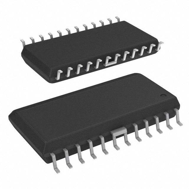
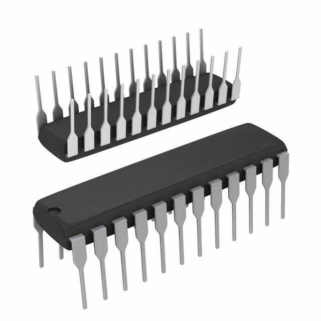
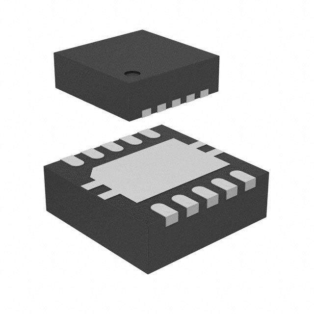
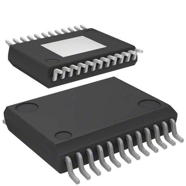
ICGOO在线商城 > 集成电路(IC) > PMIC - 电机驱动器,控制器 > DRV2603RUNT
- 型号: DRV2603RUNT
- 制造商: Texas Instruments
- 库位|库存: xxxx|xxxx
- 要求:
| 数量阶梯 | 香港交货 | 国内含税 |
| +xxxx | $xxxx | ¥xxxx |
查看当月历史价格
查看今年历史价格
DRV2603RUNT产品简介:
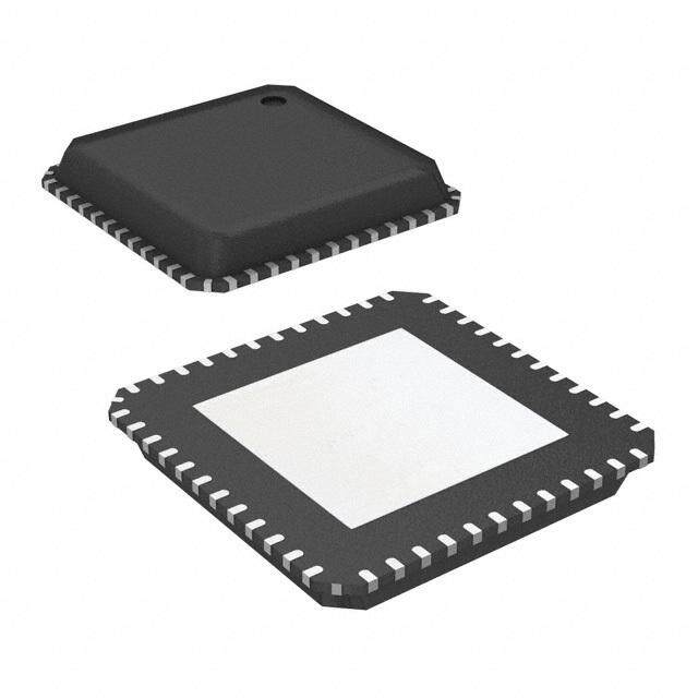
ICGOO电子元器件商城为您提供DRV2603RUNT由Texas Instruments设计生产,在icgoo商城现货销售,并且可以通过原厂、代理商等渠道进行代购。 DRV2603RUNT价格参考¥12.60-¥17.28。Texas InstrumentsDRV2603RUNT封装/规格:PMIC - 电机驱动器,控制器, 电机驱动器 功率 MOSFET 并联,PWM 10-QFN(2x2)。您可以下载DRV2603RUNT参考资料、Datasheet数据手册功能说明书,资料中有DRV2603RUNT 详细功能的应用电路图电压和使用方法及教程。
| 参数 | 数值 |
| 产品目录 | 集成电路 (IC)半导体 |
| 描述 | IC LRA/ERM HAPTIC DRIVER 10QFN马达/运动/点火控制器和驱动器 Haptic Driver w/Auto Resonance Tracking |
| 产品分类 | PMIC - 电机, 电桥式驱动器集成电路 - IC |
| 品牌 | Texas Instruments |
| 产品手册 | http://www.ti.com/litv/slos754a |
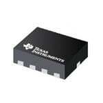
| 产品图片 | |
| rohs | 符合RoHS无铅 / 符合限制有害物质指令(RoHS)规范要求 |
| 产品系列 | 电源管理 IC,马达/运动/点火控制器和驱动器,Texas Instruments DRV2603RUNT- |
| 数据手册 | |
| 产品型号 | DRV2603RUNT |
| PCN组件/产地 | |
| 产品 | Electromechanical Drivers |
| 产品种类 | 马达/运动/点火控制器和驱动器 |
| 供应商器件封装 | 10-QFN(2x2) |
| 其它名称 | 296-34845-2 |
| 功能 | 驱动器 - 全集成,控制和功率级 |
| 包装 | 带卷 (TR) |
| 参考设计库 | http://www.digikey.com/rdl/4294959875/4294959892/949 |
| 商标 | Texas Instruments |
| 安装类型 | 表面贴装 |
| 安装风格 | SMD/SMT |
| 封装 | Reel |
| 封装/外壳 | 10-WFQFN |
| 封装/箱体 | WQFN-10 |
| 工作温度 | -40°C ~ 85°C |
| 工作电源电压 | 2.5 V to 5.2 V |
| 工作频率 | 10 kHz to 250 kHz |
| 工厂包装数量 | 250 |
| 应用 | 触觉反馈 |
| 接口 | 并联, PWM |
| 标准包装 | 250 |
| 电压-电源 | 2.5 V ~ 5.2 V |
| 电压-负载 | 2.5 V ~ 5.2 V |
| 电机类型-AC,DC | ERM、 LRA |
| 电机类型-步进 | - |
| 电流-输出 | - |
| 电源电流 | 1.5 mA |
| 类型 | ERM LRA Haptic Motor Driver |
| 系列 | DRV2603 |
| 输出配置 | 半桥, (2) 双路 |


- 商务部:美国ITC正式对集成电路等产品启动337调查
- 曝三星4nm工艺存在良率问题 高通将骁龙8 Gen1或转产台积电
- 太阳诱电将投资9.5亿元在常州建新厂生产MLCC 预计2023年完工
- 英特尔发布欧洲新工厂建设计划 深化IDM 2.0 战略
- 台积电先进制程称霸业界 有大客户加持明年业绩稳了
- 达到5530亿美元!SIA预计今年全球半导体销售额将创下新高
- 英特尔拟将自动驾驶子公司Mobileye上市 估值或超500亿美元
- 三星加码芯片和SET,合并消费电子和移动部门,撤换高东真等 CEO
- 三星电子宣布重大人事变动 还合并消费电子和移动部门
- 海关总署:前11个月进口集成电路产品价值2.52万亿元 增长14.8%
.jpg)



PDF Datasheet 数据手册内容提取
Product Sample & Technical Tools & Support & Reference Folder Buy Documents Software Community Design DRV2603 SLOS754C–JUNE2012–REVISEDAUGUST2016 DRV2603 Haptic Drive With Auto-Resonance Detection for Linear Resonance Actuators (LRA) 1 Features 3 Description • FlexibleHaptic/VibraDriver The DRV2603 is a haptic driver designed specifically 1 to solve common obstacles in driving both Linear – LRA(LinearResonanceActuator) Resonance Actuator (LRA) and Eccentric Rotating – ERM(EccentricRotatingMass) Mass (ERM) haptic elements. The DRV2603 is • AutoResonanceTrackingforLRA designed for low latency, high efficiency, and more drive strength for actuators commonly used for tactile – NoFrequencyCalibrationRequired feedbackintheportablemarket. – AutomaticDriveCommutation LRA actuators typically have a narrow frequency – AutomaticBrakingAlgorithm band over which they have an adequate haptic – WideInputPWMFrequencyRange response. This frequency window is typically ±2.5 Hz • ConstantVibrationStrengthOverSupply wide or less, so driving an LRA actuator presents a challenge. The DRV2603 solves this problem by • AutomaticInputLevelTranslation employing auto resonance tracking, which • 0%to100%DutyCycleControlRange automatically detects and tracks the LRA resonant • FastStartUpTime frequency in real time. This means that any input PWM frequency within the input range (10 kHz to 250 • DifferentialDrivefromSingle-EndedInput kHz) will automatically produce the correct resonant • WideSupplyVoltageRangeof2.5Vto5.2V output frequency. As an additional benefit, the • ImmersionTouchSense®3000Compatible DRV2603 implements an automatic braking algorithm • 1.8-VCompatible,5-VTolerantDigitalPins to prevent LRA ringing at the end of waveforms, leavingtheuserwithacrisphapticsensation. • Availableina2mm×2mm× 0.75mmLeadless QFNPackage(RUN) ForbothERMandLRAactuators,theautomaticinput level translation solves issues with low voltage PWM 2 Applications sources without adding additional external components, so if the digital I/O levels vary, the • MobilePhonesandTablets output voltage does not change. The DRV2603 also • WatchesandWearableTechnology has supply correction that ensures no supply regulation is required for constant vibration strength, • RemoteControls,Mice,andPeripheralDevices allowinganefficient,direct-batteryconnection. • ElectronicPointofSale(ePOS) • VibrationAlertsandNotifications DeviceInformation(1) • Touch-EnabledDevices PARTNUMBER PACKAGE BODYSIZE(NOM) • IndustrialHuman-MachineInterfaces DRV2603 WQFN(10) 2.00mm×2.00mm (1) For all available packages, see the orderable addendum at theendofthedatasheet. DRV2603BlockDiagram VDD Thermal VDD Supply Correction Shutdown OUT+ CVDD Overcurrent Gate Shutdown Drive EN LRA LRA / ERM Control Engine BDaectke-cEtMionF M ERoMr VDD OUT- PWM Gate Level Correction Drive GND Copyright © 2016, Texas Instruments Incorporated 1 An IMPORTANT NOTICE at the end of this data sheet addresses availability, warranty, changes, use in safety-critical applications, intellectualpropertymattersandotherimportantdisclaimers.PRODUCTIONDATA.
DRV2603 SLOS754C–JUNE2012–REVISEDAUGUST2016 www.ti.com Table of Contents 1 Features.................................................................. 1 8.4 DeviceFunctionalModes..........................................9 2 Applications........................................................... 1 9 ApplicationandImplementation........................ 11 3 Description............................................................. 1 9.1 ApplicationInformation............................................11 4 RevisionHistory..................................................... 2 9.2 TypicalApplication .................................................11 5 PinConfigurationandFunctions......................... 3 10 PowerSupplyRecommendations..................... 14 10.1 DecouplingCapacitor............................................14 6 Specifications......................................................... 3 11 Layout................................................................... 14 6.1 AbsoluteMaximumRatings......................................3 6.2 ESDRatings..............................................................3 11.1 LayoutGuidelines.................................................14 6.3 RecommendedOperatingConditions.......................4 11.2 LayoutExample....................................................14 6.4 ThermalInformation..................................................4 12 DeviceandDocumentationSupport................. 15 6.5 ElectricalCharacteristics...........................................4 12.1 DeviceSupport......................................................15 6.6 TypicalCharacteristics..............................................5 12.2 DocumentationSupport........................................15 7 ParameterMeasurementInformation..................6 12.3 ReceivingNotificationofDocumentationUpdates15 7.1 TestSetupforGraphs...............................................6 12.4 CommunityResources..........................................15 7.2 AlternateTestSetup.................................................6 12.5 Trademarks...........................................................15 12.6 ElectrostaticDischargeCaution............................15 8 DetailedDescription.............................................. 7 12.7 Glossary................................................................15 8.1 Overview...................................................................7 13 Mechanical,Packaging,andOrderable 8.2 FunctionalBlockDiagram.........................................7 Information........................................................... 15 8.3 FeatureDescription...................................................7 4 Revision History ChangesfromRevisionB(September2015)toRevisionC Page • AutoResonanceEngineforLRA,changedtextFrom:"trackingrangeforLRAdevicesis140Hzto140Hz"To: "trackingrangeforLRAdevicesis140Hzto220Hz.".......................................................................................................... 8 ChangesfromRevisionA(January2014)toRevisionB Page • AddedPinConfigurationandFunctionssection,ESDRatingstable,FeatureDescriptionsection,DeviceFunctional Modes,ApplicationandImplementationsection,PowerSupplyRecommendationssection,Layoutsection,Device andDocumentationSupportsection,andMechanical,Packaging,andOrderableInformationsection .............................. 1 ChangesfromOriginal(June2012)toRevisionA Page • Changedfrom1pagedatasheettofulldatasheetinproductfolder.................................................................................... 1 2 SubmitDocumentationFeedback Copyright©2012–2016,TexasInstrumentsIncorporated ProductFolderLinks:DRV2603
DRV2603 www.ti.com SLOS754C–JUNE2012–REVISEDAUGUST2016 5 Pin Configuration and Functions RUNPackage 10-PinWQFN TopView GND EN 1 10 9 OUT+ PWM 2 8 GND LRA/ERM 3 7 VDD NC 4 6 OUT- 5 GND PinFunctions PIN I/O/P(1) DESCRIPTION NAME NO. EN 1 I Deviceenable GND 5,8,10 P Supplyground LRA/ERM 3 I Modeselection.ERM=Low,LRA=High NC 4 I NoConnection OUT+ 9 O Positivehapticdriverdifferentialoutput OUT– 6 O Negativehapticdriverdifferentialoutput PWM 2 I Inputsignal VDD 7 P SupplyInput(2.5Vto5.5V) (1) I=Input,O=Output,P=Power 6 Specifications 6.1 Absolute Maximum Ratings(1) overoperatingfree-airtemperaturerange,T =25°C(unlessotherwisenoted) A MIN MAX UNIT Supplyvoltage VDD –0.3 6 V V Inputvoltage EN,PWM,LRA/ERM –0.3 V +0.3 V I DD T Operatingfree-airtemperaturerange –40 85 °C A T Operatingjunctiontemperaturerange –40 150 °C J T Storagetemperaturerange –65 150 °C stg (1) StressesbeyondthoselistedunderAbsoluteMaximumRatingsmaycausepermanentdamagetothedevice.Thesearestressratings only,whichdonotimplyfunctionaloperationofthedeviceattheseoranyotherconditionsbeyondthoseindicatedunderRecommended OperatingConditions.Exposuretoabsolute-maximum-ratedconditionsforextendedperiodsmayaffectdevicereliability. 6.2 ESD Ratings VALUE UNIT Electrostatic Humanbodymodel(HBM),perANSI/ESDA/JEDECJS-001(1) ±2000 V V (ESD) discharge Charged-devicemodel(CDM),perJEDECspecificationJESD22-C101(2) ±500 (1) JEDECdocumentJEP155statesthat500-VHBMallowssafemanufacturingwithastandardESDcontrolprocess. (2) JEDECdocumentJEP157statesthat250-VCDMallowssafemanufacturingwithastandardESDcontrolprocess. Copyright©2012–2016,TexasInstrumentsIncorporated SubmitDocumentationFeedback 3 ProductFolderLinks:DRV2603
DRV2603 SLOS754C–JUNE2012–REVISEDAUGUST2016 www.ti.com 6.3 Recommended Operating Conditions MIN TYP MAX UNIT V Supplyvoltage VDD 2.5 5.2 V DD f PWMInputfrequency 10 250 kHz PWM R LoadImpedance V =5.2V 8 Ω L DD F SupportedLRAfrequency AutoresonancetrackingrangeforLRA 140 220 Hz 0 V Digitalinputlowvoltage EN,PWM,LRA/ERM 0.6 V IL V Digitalinputhighvoltage EN,PWM,LRA/ERM 1.2 V IH Operatingfree-airtemperature T -40 85 °C A range 6.4 Thermal Information DRV2603 THERMALMETRIC(1) RUN(WQFN) UNIT 10PINS R Junction-to-ambientthermalresistance 153.7 °C/W θJA R Junction-to-case(top)thermalresistance 86 °C/W θJC(top) R Junction-to-boardthermalresistance 70.4 °C/W θJB ψ Junction-to-topcharacterizationparameter 1.3 °C/W JT ψ Junction-to-boardcharacterizationparameter 70.4 °C/W JB (1) Formoreinformationabouttraditionalandnewthermalmetrics,seetheSemiconductorandICPackageThermalMetricsapplication report. 6.5 Electrical Characteristics T =25°C,V =3.6V(unlessotherwisenoted) A DD PARAMETER TESTCONDITIONS MIN TYP MAX UNIT |I | Digitalinputlowcurrent EN,PWM,LRA/ERM V =5.0V,V =0V 1 µA IL DD IN EN V =5.0V,V =V 6 µA DD IN DD |I | Digitalinputhighcurrent IH PWM,LRA/ERM V =5.0V,V =V 3 µA DD IN DD I Shutdowncurrent V =0V 0.3 3 µA SD EN I Quiescentcurrent V =V ,ERMMode,50%dutycycleinput,Noload 1.7 2.5 mA DDQ EN DD R Outputimpedanceinshutdown OUT+toGND,OUT–toGND 15 kΩ OUT t Start-uptime TimefromENhightooutputsignal 1.3 ms SU f PWMoutputfrequency 19.5 20.3 21.5 kHz SW DutyCycle=100%,LRAMode,Load=25ΩLRA 55 Averagebatterycurrentduring IBAT,AVG operation DutyCycle=80%,ERMMode,RL=17Ω,2Vrated 59 mA ERM R Draintosourceresistance,high-side 1.05 Ω DS-HS R Draintosourceresistance,low-side 0.85 Ω DS-LS DutyCycle=100%,LRAMode,Load=25ΩLRA 2.2 V RMS V Differentialoutputvoltage OUT DutyCycle=100%,ERMMode,R =20ΩERM 3.3 V L Thermalthreshold 145 °C ThermalHysteresis 18 °C 4 SubmitDocumentationFeedback Copyright©2012–2016,TexasInstrumentsIncorporated ProductFolderLinks:DRV2603
DRV2603 www.ti.com SLOS754C–JUNE2012–REVISEDAUGUST2016 6.6 Typical Characteristics VDD = 4.2 V EN, PWM VDD = 3.6 V OUT+ (Filtered) LRA Mode OUT+ LRA Mode OUT− (Filtered) Startup Time = 1.3 ms OUT− Full−Scale Input [OUT+] − [OUT−] (Filtered) VOUT(P-P) = 2.2 VRMS Voltage − (1V/div) Voltage − (1V/div) 0 1m 2m 3m 4m 5m 6m 7m 8m 9m 10m 0 5m 10m 15m 20m 25m 30m 35m 40m 45m 50m t − Time − s t − Time − s Figure1.StartupWaveform Figure2.LRAFull-ScaleDrive VDD = 3.6 V EN VDD = 3.6 V EN LRA Mode PWM ERM Mode PWM Accelerometer Accelerometer [OUT+] − [OUT−] (Filtered) [OUT+] − [OUT−] (Filtered) Voltage − (2V/div) Voltage − (2V/div) 0 40m 80m 120m 160m 200m 0 40m 80m 120m 160m 200m t − Time − s t − Time − s Figure3.LRAClick Figure4.ERMClick VDD = 3.6 V EN VDD = 3.6 V EN LRA Mode PWM (Filtered) ERM Mode PWM (Filtered) PWM Sequence = [OUT+] − [OUT−] (Filtered) PWM Sequence = [OUT+] − [OUT−] (Filtered) {100%, 87.5%, 75%, 62.5%, 0%} {100%, 87.5%, 75%, 62.5%, 0%} Voltage − (2V/div) Voltage − (2V/div) 0 40m 80m 120m 160m 200m 0 40m 80m 120m 160m 200m t − Time − s t − Time − s Figure5.LRAPWMModulation Figure6.ERMPWMModulation Copyright©2012–2016,TexasInstrumentsIncorporated SubmitDocumentationFeedback 5 ProductFolderLinks:DRV2603
DRV2603 SLOS754C–JUNE2012–REVISEDAUGUST2016 www.ti.com 7 Parameter Measurement Information 7.1 Test Setup for Graphs Withnooutputfilter,theoutputwaveformfromthe DRV2603lookssimilartoFigure1.Theoutputsignalcontains both a high frequency PWM component and a fundamental drive component which causes motion in the actuator. To measure or observe the fundamental drive component, a low-pass filter must be used to eliminate the PWM component. The digital filter function on a digital oscilloscope was utilized in the rest of the Typical Characteristicfigures.A1storder,low-passfiltercornerbetween1kHzand3.5kHzisrecommended. OUT+ Ch1 Ch1-Ch2 ERM (Differential) or Ch2 with Digital LRA Low-Pass Filter Oscilloscope OUT– Figure7. TestSetupforGraphs 7.2 Alternate Test Setup If a digital oscilloscope with digital filtering is not available, a 1st order, low-pass, RC filter network can be used instead. Care must be taken not to use a filter impedance that is too low. This can interfere with the back-EMF behavior of the actuator and corrupt the operation of the auto resonance function. A recommended circuit is showninFigure8. 100kΩ OUT+ ERM 470 pF Ch1 Or Ch1-Ch2 LRA Ch2 (Differential) OUT– 100kΩ Oscilloscope 470 pF Figure8. AlternateTestSetup 6 SubmitDocumentationFeedback Copyright©2012–2016,TexasInstrumentsIncorporated ProductFolderLinks:DRV2603
DRV2603 www.ti.com SLOS754C–JUNE2012–REVISEDAUGUST2016 8 Detailed Description 8.1 Overview The DRV2603 is a haptic and vibratory driver designed specifically to meet the needs of haptic and vibration applicationsintheportablemarket.TheDRV2603hastwomodesofoperation,ERMmodeandLRAmode.ERM mode is designed to drive Eccentric Rotating Mass motors, which are generally DC motors of the bar or coin type. LRA mode is designed to drive Linear Resonance Actuators, also known as linear vibrators, which require an alternating signal that commutates at or very near the natural mechanical resonance frequency of the actuator. These actuators present a unique control challenge that is solved in the DRV2603 by auto resonance tracking. 8.2 Functional Block Diagram VDD VDD Thermal Supply Correction Shutdown OUT+ C VDD Overcurrent Gate Shutdown Drive EN LRA Control Engine Back-EMF M or LRA / ERM Detection ERM VDD OUT- PWM Gate Drive Level Correction GND Copyright © 2016, Texas Instruments Incorporated 8.3 Feature Description 8.3.1 SupplyVoltageRejectionforConstantVibrationStrength The DRV2603 features power supply feedback, so no external supply regulation is required. If the supply voltage drifts over time (due to battery discharge, for example), the vibration strength will remain the same so long as thereisenoughsupplyvoltagetosustaintherequiredoutputvoltage.The DRV2603canbeconnecteddirectlyto thebattery. 8.3.2 Low-VoltageControlLogicforConstantVibrationStrength The PWM input uses a digital level-shifter, so as long as the input voltage meets the V and V levels, the IH IL vibration strength will remain the same even if the digital levels were to vary. These benefits apply to both ERM modeandLRAmode. 8.3.3 ThermalProtection The DRV2603 has thermal protection that will shut down the device to prevent internal overheating. See the Specificationsfortypicalovertemperaturethresholds. Copyright©2012–2016,TexasInstrumentsIncorporated SubmitDocumentationFeedback 7 ProductFolderLinks:DRV2603
DRV2603 SLOS754C–JUNE2012–REVISEDAUGUST2016 www.ti.com Feature Description (continued) 8.3.4 OvercurrentProtection The DRV2603 has overcurrent protection that is useful in preventing damage from short conditions. The overcurrent protection monitors current from VDD, GND, OUT+, and OUT-. See the Specifications for typical overcurrentthresholds. 8.3.5 LinearResonanceActuators(LRA) Linear Resonant Actuators, or LRAs, only vibrate effectively at their resonant frequency. LRAs have a high-Q frequency response due to which there is a rapid drop in vibration performance at offsets of 2 to 3 Hz from the resonant frequency. Many factors also cause a shift or drift in the resonant frequency of the actuator such as temperature, aging, the mass the product to which the LRA is mounted, and in the case of a portable product, the manner in which it is held. Furthermore, as the actuator is driven to its maximum allowed voltage, many LRAs will shift several Hz in frequency due to mechanical compression. All of these factors make a real-time trackingauto-resonantalgorithmcriticalwhendrivingLRAtoachieveconsistent,optimizedperformance. g n - o ati r e el c c A Frequency - Hz f RESONANCE Figure9. TypicalLRAResponse 8.3.6 AutoResonanceEngineforLRA No frequency calibration or actuator training is required to use the DRV2603. The DRV2603 auto resonance engine tracks the resonant frequency of an LRA in real time. If the resonant frequency shifts in the middle of a waveform for any reason, the engine will track it cycle to cycle. The auto resonance engine accomplishes this by constantly monitoring the back-EMF of the actuator. The DRV2603 tracking range for LRA devices is 140 Hz to 220Hz. 8.3.7 EccentricRotatingMassMotors(ERM) Eccentric Rotating Mass motors, or ERMs, are typically DC-controlled motors of the bar or coin type. ERMs can be driven in the clockwise direction or counter-clockwise depending on the polarity of voltage across its two terminals. Bi-directional drive is made possible in a single-supply system by differential outputs that are capable of sourcing and sinking current. This feature helps eliminate long vibration tails which are undesirable in haptic feedbacksystems.. Figure10. ReversalofMotorDirection 8 SubmitDocumentationFeedback Copyright©2012–2016,TexasInstrumentsIncorporated ProductFolderLinks:DRV2603
DRV2603 www.ti.com SLOS754C–JUNE2012–REVISEDAUGUST2016 Feature Description (continued) Another common approach to driving DC motors is the concept of overdrive voltage. To overcome the inertia of the motor's mass, they are often overdriven for a short amount of time before returning to the motor's rated voltage to sustain the motor's rotation. Negative overdrive is also used to stop (or brake) an ERM quickly by reversingthemagneticfieldofthedrivingcoil(s). 8.3.8 EdgeRateControl The DRV2603 output driver implements Edge Rate Control (ERC). This ensures that the rise and fall characteristics of the output drivers do not emit levels of radiation that could interfere with other circuitry common inmobileandportableplatforms.BecauseofERC,nooutputfilterorferritesarenecessary. 8.4 Device Functional Modes 8.4.1 LRAMode When in LRA mode, the DRV2603 employs a simple control scheme that is designed to be compatible with ERM mode signaling. A 100% input duty cycle gives full vibration strength, and a 0% to 50% input duty cycle gives no vibration strength. The auto resonance detection algorithm takes care of the physical layer signaling and commutation required by linear resonance actuators. The DRV2603 implements closed-loop operation comprising a simple feedback loop. If the back-EMF feedback tells the device that the vibration is too low relative to the input duty cycle, the DRV2603 will increase the vibration strength. If the back-EMF feedback tells the device that the vibration is too high relative to the input duty cycle, the DRV2603 automatically enforces a braking algorithm. It follows that a 0% to 50% input duty cycle will always enforce braking until the LRA is no longer moving. This form of signaling is used to preserve the same input format for both ERM and LRA drive; therefore,nosoftwarechangesarerequiredwhenswitchingbetweenERMsandLRAswiththe DRV2603. Steady-State Output Drive 2.2Vrms 1.1Vrms Full Braking Input 0% 50% 75% 100% PWM Input Duty Cycle Figure11. LRAMode The exact full-scale output voltage depends on the physical construction of the LRA itself. Some LRA devices give a small amount of back-EMF during full scale vibration, and other LRA devices give a much larger amount. A nominal full-scale output value is 2.2 V , but it can typically vary as much as +/- 10% depending on the RMS actuator's physical design. The output voltage can be approximated by the following equation between 50% and 100%inputdutycycle. éInputDutyCycle% ù VOUT(RMS)=VOUT(FULL-SCALE) ê -1ú ë 50 û (1) Since the DRV2603 includes constant output drive over supply voltage, the output PWM duty cycle will be adjustedsothattherelationshipintheaboveequationwillholdtrueregardlessofthesupplyvoltage. Copyright©2012–2016,TexasInstrumentsIncorporated SubmitDocumentationFeedback 9 ProductFolderLinks:DRV2603
DRV2603 SLOS754C–JUNE2012–REVISEDAUGUST2016 www.ti.com Device Functional Modes (continued) 8.4.2 ERMMode The DRV2603 is a compact, cost-effective driver solution for ERM motors. Most competing solutions require external components for biasing or level-shifting, but the DRV2603 requires only one decoupling capacitor giving a total approximate circuit size of 2 mm by 2 mm. This small solution size still comes packed with features such asalevel-shiftedinput,differentialoutputsforbraking,constantdrivestrengthoversupply,edgeratecontrol,and awideinputPWMfrequencyrange. WheninERMmode,the DRV2603employsasimplecontrolscheme.A100%inputdutycyclegivesfull-strength forward rotation, a 50% input duty cycle give no rotation strength, and a 0% duty cycle give full-strength reverse rotation. Forcing the motor velocity towards reverse rotation is used to implement motor braking in ERMs. By stringing together various duty cycles over varying amounts of time, a haptic motor control signal will be constructedattheoutputtopreciselydrivethemotor. Output Drive 3.3V 0V -3.3V Input 0% 50% 100% PWM Input Duty Cycle Figure12. ERMMode The full-scale, open-load output voltage of the DRV2603 in ERM mode is 3.6V. The output stage has a total nominal R of 1.9 Ω. When driving a 20 Ω ERM at full-scale, the differential voltage seen at the outputs is DS approximately3.3V.Whendrivinga10 ΩERMatfull-scale,theoutputvoltageisapproximately3.0V. Thevoltageseenattheoutputsasafunctionofinputdutycycleisgivenbythisequation. éInputDutyCycle% ù VOUT =VOUT(FULL-SCALE) ê -1ú ë 50 û (2) Since the DRV2603 includes constant output drive over supply voltage, the output PWM duty cycle will be adjusted so that the relationship in the above equation will hold true regardless of the supply voltage. The output dutycycleinERMmodecanbeapproximatedbythefollowingequation. V éInputDutyCycle% ù OUT(FULL-SCALE) OutputDutyCycle(%)= ê -1ú 100% VDD ë 50 û (3) 10 SubmitDocumentationFeedback Copyright©2012–2016,TexasInstrumentsIncorporated ProductFolderLinks:DRV2603
DRV2603 www.ti.com SLOS754C–JUNE2012–REVISEDAUGUST2016 9 Application and Implementation NOTE Information in the following applications sections is not part of the TI component specification, and TI does not warrant its accuracy or completeness. TI’s customers are responsible for determining suitability of components for their purposes. Customers should validateandtesttheirdesignimplementationtoconfirmsystemfunctionality. 9.1 Application Information The DRV2603 is designed to drive ERM and LRA actuators used for haptic feedback. ERM and LRA actuators can be used for numerous haptic feedback applications including vibration alerts, advanced vibration communication,buttonreplacement,andtactilefeedbackfortouchsurfaceorscreens. The DRV2603 output is controlled using PWM input. The duty-cycle of the PWM determines the amplitude of the output waveform. By varying the duty cycle, advanced haptic patterns and sequences can be created such as click,bumps,pulses,rampsandmanymore. If a PWM port is not available, the DRV2603 PWM pin can be controlled with a GPIO; however, the DRV2603 will only function as an ON-OFF driver. In the case of an ERM, when the GPIO is ON the output is 100% and whentheGPIOisOFFtheoutputis-100%(oppositedirection).InthecaseofanLRA,whentheGPIOisONthe output is 100% and when the GPIO is OFF the driver automatically brakes and will automatically bring the actuatortorest. 9.2 Typical Application The DRV2603 supports both ERM and LRA actuators. The operating mode can be selected by pulling the LRA/ERM pin either HIGH or LOW. Figure 13 shows the LRA configuration and Figure 14 shows the ERM configuration. DRV2603 Application Processor GPIO EN OUT+ PWM PWM GND Linear Vibrator (LRA) VDD LRA/ERM VDD 2.5V to5.2V OUT- C VDD Copyright©2016,TexasInstrumentsIncorporated Figure13. SystemDiagramforLRA Copyright©2012–2016,TexasInstrumentsIncorporated SubmitDocumentationFeedback 11 ProductFolderLinks:DRV2603
DRV2603 SLOS754C–JUNE2012–REVISEDAUGUST2016 www.ti.com Typical Application (continued) DRV2603 Application Processor GPIO EN OUT+ PWM PWM GND DC Motor (ERM) GND LRA/ERM VDD 2.5V to5.2V OUT- C VDD Copyright©2016,TexasInstrumentsIncorporated Figure14. SystemDiagramforERM 9.2.1 DesignRequirements ThisdesignassumesthevalueslistedinTable1. Table1.DesignParameters DESIGNPARAMETER EXAMPLEVALUE Interface PWM ActuatorType ERM/LRA InputPowerSource Battery 9.2.2 DetailedDesignProcedure 9.2.2.1 ActuatorSelection The actuator decision is based on many factors including cost, form factor, vibration strength, power consumptionrequirements,hapticsharpness,reliability,andaudiblenoiseperformance.Theactuatorselectionis one of the most important design considerations of a haptic system and therefore the actuator should be the first componenttoconsiderwhendesigningthesystem. Thefollowingcanbeusedtoselecttheminimumrequiredsupplyvoltage. 1. Find the rated and/or maximum operating voltage in the actuator datasheet; some actuator datasheets may onlyhavetheratedvoltagelisted. 2. Using the larger of the rated and maximum operating voltage, add 250mV to get the minimum operating voltage.Adding250mVprovidesoperatingheadroomtoaccountforinternaldriverlosses. 3. Checkthesupplyvoltagetoensurethatthedesiredoutputisachieved. A minimum supply current is also required based on the load. To ensure enough current can be sourced divide the supply voltage above by the load resistance in the actuator datasheet. Compare this number with the current capabilityofthebatteryorvoltagesupply. 9.2.2.2 PowerSupplySelection The DRV2603 supports supply voltages from 2.5 to 5.2V. The DRV2603 can be directly connected to many battery types including common batteries like Lithium-Ion and Lithium-Polymer. The supply rejection feature of theDRV2603eliminatestheneedforavoltageregulatorbetweenthebatteryandVDD. 9.2.2.3 SendingaHapticEffect Sending a haptic effect with the DRV2603 is straightforward. The procedure is the same for both ERM and LRA drive. The ERM/LRA pin should be tied high or low as shown in the system diagrams. Optimum performance is achievedbyusingthefollowingsteps. 12 SubmitDocumentationFeedback Copyright©2012–2016,TexasInstrumentsIncorporated ProductFolderLinks:DRV2603
DRV2603 www.ti.com SLOS754C–JUNE2012–REVISEDAUGUST2016 1. At or very near the same time, bring the EN pin high and start sourcing PWM waveform. No delays are required. The best startup behavior is usually achieved when momentarily overdriving the actuator for 20 ms to50ms.Referencethespecificationsoftheactuatorforoptimumoverdrivecharacteristics. 2. ChangethePWMlevelasneededtoachievethedesiredeffect. 3. When the effect is complete, set the PWM duty cycle to 0% if braking is desired. The EN pin must remain high to actively brake the actuator. When braking is complete, set the EN pin low, concluding the haptic effect. When braking an ERM, the user should take care not to brake the actuator for too long, or counter- rotation can occur. When braking an LRA, the auto-resonance engine automatically drives the actuator to zerovibration,sonosignificantreverse-phasevibrationwilleveroccur. 9.2.3 ApplicationCurves VDD = 3.6 V EN VDD = 3.6 V EN LRA Mode PWM ERM Mode PWM Accelerometer Accelerometer [OUT+] − [OUT−] (Filtered) [OUT+] − [OUT−] (Filtered) Voltage − (2V/div) Voltage − (2V/div) 0 40m 80m 120m 160m 200m 0 40m 80m 120m 160m 200m t − Time − s t − Time − s Figure15.LRAClick Figure16.ERMClick VDD = 3.6 V EN VDD = 3.6 V EN LRA Mode PWM (Filtered) ERM Mode PWM (Filtered) PWM Sequence = [OUT+] − [OUT−] (Filtered) PWM Sequence = [OUT+] − [OUT−] (Filtered) {100%, 87.5%, 75%, 62.5%, 0%} {100%, 87.5%, 75%, 62.5%, 0%} Voltage − (2V/div) Voltage − (2V/div) 0 40m 80m 120m 160m 200m 0 40m 80m 120m 160m 200m t − Time − s t − Time − s Figure17.LRAPWMModulation Figure18.ERMPWMModulation Copyright©2012–2016,TexasInstrumentsIncorporated SubmitDocumentationFeedback 13 ProductFolderLinks:DRV2603
DRV2603 SLOS754C–JUNE2012–REVISEDAUGUST2016 www.ti.com 10 Power Supply Recommendations The DRV2603 can operate from 2.5V to 5.2V. The DRV2603 VDD pin can be connected directly to a battery to eliminatealinearregulatororswitchingpowersupply.Asmalldecouplingcapacitorshouldbeplacedclosetothe DRV2603VDDpin. 10.1 Decoupling Capacitor The DRV2603 has a switching output stage which pulls transient currents through the VDD pin. A 0.1 µF, low equivalent-series-resistance (ESR) decoupling capacitor of the X5R or X7R type is recommended for smooth operationoftheoutputdriverandthedigitalportionofthedevice. 11 Layout 11.1 Layout Guidelines ThefollowinglistcontainsguidelinesfortheDRV2603layout: • Thedecouplingcapacitorforthepowersupplyshouldbeplacedclosetothedevicepin(VDD). • ThesupplygroundshouldbeconnectedtoallGNDpins 11.2 Layout Example Figure19showstherecommendedlayoutfortheDRV2603. GND D OUT+ N EN G OUT+ PWM GND Via CVDD LRA/ERM VDD VDD NC D OUT- GN OUT- GND Figure19. DRV2603LayoutExample 14 SubmitDocumentationFeedback Copyright©2012–2016,TexasInstrumentsIncorporated ProductFolderLinks:DRV2603
DRV2603 www.ti.com SLOS754C–JUNE2012–REVISEDAUGUST2016 12 Device and Documentation Support 12.1 Device Support 12.1.1 DevelopmentSupport TheDRV2603isfeaturedinseveralTIDesigns,availableonlineat http://www.ti.com/general/docs/refdesignsearch.tsp. TI Designs are analog solutions created by TI’s applications experts and offer the theory of operation, component selection, simulation, complete PCB schematic and layout, billofmaterials,andmeasuredperformanceofmanyusefulcircuits. • HapticsEnabledGamingControllerDesign -http://www.ti.com/tool/TIDM-LPBP-HAPTOUCH • DRV2603CapacitiveTouchEvaluationModule -http://www.ti.com/tool/drv2603evm-ct 12.2 Documentation Support 12.2.1 RelatedDocumentation • HapticEnergyConsumption–SLOA194 • BenefitsofLRAAuto-ResonanceTracking -SLOA188 • Haptics:SolutionsforERMandLRAActuators -SSZB151 12.3 Receiving Notification of Documentation Updates To receive notification of documentation updates, navigate to the device product folder on ti.com. In the upper right corner, click on Alert me to register and receive a weekly digest of any product information that has changed.Forchangedetails,reviewtherevisionhistoryincludedinanyreviseddocument. 12.4 Community Resources The following links connect to TI community resources. Linked contents are provided "AS IS" by the respective contributors. They do not constitute TI specifications and do not necessarily reflect TI's views; see TI's Terms of Use. TIE2E™OnlineCommunity TI'sEngineer-to-Engineer(E2E)Community.Createdtofostercollaboration amongengineers.Ate2e.ti.com,youcanaskquestions,shareknowledge,exploreideasandhelp solveproblemswithfellowengineers. DesignSupport TI'sDesignSupport QuicklyfindhelpfulE2Eforumsalongwithdesignsupporttoolsand contactinformationfortechnicalsupport. 12.5 Trademarks E2EisatrademarkofTexasInstruments. TouchSenseisaregisteredtrademarkofImmersionCorporation. Allothertrademarksarethepropertyoftheirrespectiveowners. 12.6 Electrostatic Discharge Caution Thesedeviceshavelimitedbuilt-inESDprotection.Theleadsshouldbeshortedtogetherorthedeviceplacedinconductivefoam duringstorageorhandlingtopreventelectrostaticdamagetotheMOSgates. 12.7 Glossary SLYZ022—TIGlossary. Thisglossarylistsandexplainsterms,acronyms,anddefinitions. 13 Mechanical, Packaging, and Orderable Information The following pages include mechanical, packaging, and orderable information. This information is the most current data available for the designated devices. This data is subject to change without notice and revision of thisdocument.Forbrowser-basedversionsofthisdatasheet,refertotheleft-handnavigation. Copyright©2012–2016,TexasInstrumentsIncorporated SubmitDocumentationFeedback 15 ProductFolderLinks:DRV2603
PACKAGE OPTION ADDENDUM www.ti.com 6-Feb-2020 PACKAGING INFORMATION Orderable Device Status Package Type Package Pins Package Eco Plan Lead/Ball Finish MSL Peak Temp Op Temp (°C) Device Marking Samples (1) Drawing Qty (2) (6) (3) (4/5) DRV2603RUNR ACTIVE QFN RUN 10 3000 Green (RoHS NIPDAU Level-2-260C-1 YEAR -40 to 85 2603 & no Sb/Br) DRV2603RUNT ACTIVE QFN RUN 10 250 Green (RoHS NIPDAU Level-2-260C-1 YEAR -40 to 85 2603 & no Sb/Br) (1) The marketing status values are defined as follows: ACTIVE: Product device recommended for new designs. LIFEBUY: TI has announced that the device will be discontinued, and a lifetime-buy period is in effect. NRND: Not recommended for new designs. Device is in production to support existing customers, but TI does not recommend using this part in a new design. PREVIEW: Device has been announced but is not in production. Samples may or may not be available. OBSOLETE: TI has discontinued the production of the device. (2) RoHS: TI defines "RoHS" to mean semiconductor products that are compliant with the current EU RoHS requirements for all 10 RoHS substances, including the requirement that RoHS substance do not exceed 0.1% by weight in homogeneous materials. Where designed to be soldered at high temperatures, "RoHS" products are suitable for use in specified lead-free processes. TI may reference these types of products as "Pb-Free". RoHS Exempt: TI defines "RoHS Exempt" to mean products that contain lead but are compliant with EU RoHS pursuant to a specific EU RoHS exemption. Green: TI defines "Green" to mean the content of Chlorine (Cl) and Bromine (Br) based flame retardants meet JS709B low halogen requirements of <=1000ppm threshold. Antimony trioxide based flame retardants must also meet the <=1000ppm threshold requirement. (3) MSL, Peak Temp. - The Moisture Sensitivity Level rating according to the JEDEC industry standard classifications, and peak solder temperature. (4) There may be additional marking, which relates to the logo, the lot trace code information, or the environmental category on the device. (5) Multiple Device Markings will be inside parentheses. Only one Device Marking contained in parentheses and separated by a "~" will appear on a device. If a line is indented then it is a continuation of the previous line and the two combined represent the entire Device Marking for that device. (6) Lead/Ball Finish - Orderable Devices may have multiple material finish options. Finish options are separated by a vertical ruled line. Lead/Ball Finish values may wrap to two lines if the finish value exceeds the maximum column width. Important Information and Disclaimer:The information provided on this page represents TI's knowledge and belief as of the date that it is provided. TI bases its knowledge and belief on information provided by third parties, and makes no representation or warranty as to the accuracy of such information. Efforts are underway to better integrate information from third parties. TI has taken and continues to take reasonable steps to provide representative and accurate information but may not have conducted destructive testing or chemical analysis on incoming materials and chemicals. TI and TI suppliers consider certain information to be proprietary, and thus CAS numbers and other limited information may not be available for release. In no event shall TI's liability arising out of such information exceed the total purchase price of the TI part(s) at issue in this document sold by TI to Customer on an annual basis. Addendum-Page 1
PACKAGE OPTION ADDENDUM www.ti.com 6-Feb-2020 Addendum-Page 2
PACKAGE MATERIALS INFORMATION www.ti.com 30-May-2019 TAPE AND REEL INFORMATION *Alldimensionsarenominal Device Package Package Pins SPQ Reel Reel A0 B0 K0 P1 W Pin1 Type Drawing Diameter Width (mm) (mm) (mm) (mm) (mm) Quadrant (mm) W1(mm) DRV2603RUNR QFN RUN 10 3000 180.0 8.4 2.3 2.3 1.15 4.0 8.0 Q2 DRV2603RUNR QFN RUN 10 3000 180.0 8.4 2.3 2.3 1.15 4.0 8.0 Q2 DRV2603RUNT QFN RUN 10 250 180.0 8.4 2.3 2.3 1.15 4.0 8.0 Q2 DRV2603RUNT QFN RUN 10 250 180.0 8.4 2.3 2.3 1.15 4.0 8.0 Q2 PackMaterials-Page1
PACKAGE MATERIALS INFORMATION www.ti.com 30-May-2019 *Alldimensionsarenominal Device PackageType PackageDrawing Pins SPQ Length(mm) Width(mm) Height(mm) DRV2603RUNR QFN RUN 10 3000 210.0 185.0 35.0 DRV2603RUNR QFN RUN 10 3000 210.0 185.0 35.0 DRV2603RUNT QFN RUN 10 250 210.0 185.0 35.0 DRV2603RUNT QFN RUN 10 250 210.0 185.0 35.0 PackMaterials-Page2
None
None
IMPORTANTNOTICEANDDISCLAIMER TI PROVIDES TECHNICAL AND RELIABILITY DATA (INCLUDING DATASHEETS), DESIGN RESOURCES (INCLUDING REFERENCE DESIGNS), APPLICATION OR OTHER DESIGN ADVICE, WEB TOOLS, SAFETY INFORMATION, AND OTHER RESOURCES “AS IS” AND WITH ALL FAULTS, AND DISCLAIMS ALL WARRANTIES, EXPRESS AND IMPLIED, INCLUDING WITHOUT LIMITATION ANY IMPLIED WARRANTIES OF MERCHANTABILITY, FITNESS FOR A PARTICULAR PURPOSE OR NON-INFRINGEMENT OF THIRD PARTY INTELLECTUAL PROPERTY RIGHTS. These resources are intended for skilled developers designing with TI products. You are solely responsible for (1) selecting the appropriate TI products for your application, (2) designing, validating and testing your application, and (3) ensuring your application meets applicable standards, and any other safety, security, or other requirements. These resources are subject to change without notice. TI grants you permission to use these resources only for development of an application that uses the TI products described in the resource. Other reproduction and display of these resources is prohibited. No license is granted to any other TI intellectual property right or to any third party intellectual property right. TI disclaims responsibility for, and you will fully indemnify TI and its representatives against, any claims, damages, costs, losses, and liabilities arising out of your use of these resources. TI’s products are provided subject to TI’s Terms of Sale (www.ti.com/legal/termsofsale.html) or other applicable terms available either on ti.com or provided in conjunction with such TI products. TI’s provision of these resources does not expand or otherwise alter TI’s applicable warranties or warranty disclaimers for TI products. Mailing Address: Texas Instruments, Post Office Box 655303, Dallas, Texas 75265 Copyright © 2020, Texas Instruments Incorporated
 Datasheet下载