ICGOO在线商城 > 集成电路(IC) > PMIC - 配电开关,负载驱动器 > DRV103U

 Datasheet下载
- 型号: DRV103U
- 制造商: Texas Instruments
- 库位|库存: xxxx|xxxx
- 要求:
| 数量阶梯 | 香港交货 | 国内含税 |
| +xxxx | $xxxx | ¥xxxx |
查看当月历史价格
查看今年历史价格
DRV103U产品简介:
ICGOO电子元器件商城为您提供DRV103U由Texas Instruments设计生产,在icgoo商城现货销售,并且可以通过原厂、代理商等渠道进行代购。 DRV103U价格参考。Texas InstrumentsDRV103U封装/规格:PMIC - 配电开关,负载驱动器, 。您可以下载DRV103U参考资料、Datasheet数据手册功能说明书,资料中有DRV103U 详细功能的应用电路图电压和使用方法及教程。
| 参数 | 数值 |
| 产品目录 | 集成电路 (IC)半导体 |
| 描述 | IC LO-SIDE DRIVER PWM 8SOIC马达/运动/点火控制器和驱动器 Low Side Driver 1.5A/3A |
| 产品分类 | PMIC - 电源分配开关集成电路 - IC |
| 品牌 | Texas Instruments |
| 产品手册 | |
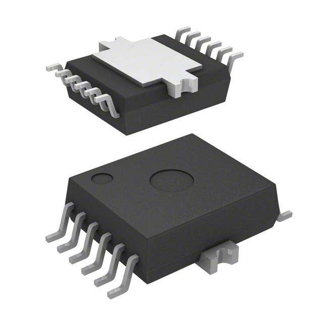
| 产品图片 |
|
| rohs | 符合RoHS无铅 / 符合限制有害物质指令(RoHS)规范要求 |
| 产品系列 | 电源管理 IC,马达/运动/点火控制器和驱动器,Texas Instruments DRV103U- |
| 数据手册 | |
| 产品型号 | DRV103U |
| Rds(On) | - |
| 产品 | Electromechanical Drivers |
| 产品目录页面 | |
| 产品种类 | 马达/运动/点火控制器和驱动器 |
| 供应商器件封装 | 8-SOIC |
| 其它名称 | 296-11622 |
| 包装 | 管件 |
| 单位重量 | 76 mg |
| 商标 | Texas Instruments |
| 安装类型 | 表面贴装 |
| 安装风格 | SMD/SMT |
| 导通电阻 | - |
| 封装 | Tube |
| 封装/外壳 | 8-SOIC(0.154",3.90mm 宽) |
| 封装/箱体 | SOIC-8 |
| 工作温度 | - 40 C to + 85 C |
| 工作电源电压 | 8 V to 32 V |
| 工厂包装数量 | 75 |
| 开关类型 | 继电器, 螺线管驱动器 |
| 接口 | 开/关 |
| 标准包装 | 75 |
| 比率-输入:输出 | 1:1 |
| 特性 | 内部 PWM,状态标志 |
| 电压-电源 | 8 V ~ 32 V |
| 电压-电源(Vcc/Vdd) | 不需要 |
| 电压-负载 | 8 V ~ 32 V |
| 电流-峰值输出 | 3.5A |
| 电流-输出/通道 | 1.5A |
| 电流-输出(最大值) | 1.5A |
| 类型 | PWM Low Side Driver |
| 系列 | DRV103 |
| 负载电压 | 8 V to 32 V |
| 输入类型 | 非反相 |
| 输出数 | 1 |
| 输出电流 | 3 A |
| 输出端数量 | 1 |
| 输出类型 | N 通道 |
| 输出配置 | 低端 |


PDF Datasheet 数据手册内容提取
DRV103 DRV103 DRV103 SBVS029A – JUNE 2001 PWM LOW-SIDE DRIVER (1.5A and 3A) for Solenoids, Coils, Valves, Heaters, and Lamps FEATURES DESCRIPTION (cid:1) HIGH OUTPUT DRIVE: 1.5A and 3A Versions The DRV103 is a low-side DMOS power switch employing (cid:1) WIDE SUPPLY RANGE: +8V to +32V a pulse-width modulated (PWM) output. Its rugged design is optimized for driving electromechanical devices such as (cid:1) COMPLETE FUNCTION valves, solenoids, relays, actuators, motors, and positioners. Digitally Controlled Input The DRV103 is also ideal for driving thermal devices such PWM Output as heaters, coolers, and lamps. PWM operation conserves Adjustable Internal Oscillator: 500Hz to 100kHz power and reduces heat rise, resulting in higher reliability. In Adjustable Delay and Duty Cycle addition, adjustable PWM allows fine control of the power (cid:1) FULLY PROTECTED delivered to the load. DC-to-PWM output delay time and Thermal and Current Limit Shutdown with oscillator frequency are also externally adjustable. Status OK Indicator Flag The DRV103 can be set to provide a strong initial closure, (cid:1) PACKAGES: SO-8 and PowerPAD™ SO-8 automatically switching to a “soft” hold mode for power savings. A resistor, analog voltage, or Digital-to-Analog APPLICATIONS (D/A) converter can control the duty cycle. An output OK flag indicates when thermal shutdown or over current occurs. (cid:1) ELECTROMECHANICAL DRIVER: Two packages provide a choice of output current: Solenoids, Valves, Positioners, Actuators, 1.5A (SO-8) or 3A (PowerPAD™ SO-8 with exposed metal Relays, Power Contactor Coils, Heaters, Lamps heat sink). (cid:1) HYDRAULIC AND PNEUMATICS SYSTEMS The DRV103 is specified for –40°C to +85°C. (cid:1) PART HANDLERS AND SORTERS (cid:1) CHEMICAL PROCESSING (cid:1) ENVIRONMENTAL MONITORING AND HVAC Status OK (cid:1) THERMOELECTRIC COOLERS Flag +V S (cid:1) DC MOTOR SPEED CONTROLS (cid:1) MEDICAL AND SCIENTIFIC ANALYZERS Flyback (cid:1) FUEL INJECTOR DRIVERS DRV103 Thermal Shutdown DMOS ESD Diode Load Over Current OUT PowerPAD is a trademark of Texas Instruments. VREF Oscillator DMOS Input PWM On Delay GND Off Delay Osc Freq Duty Cycle Adj Adj Adj C R R D FREQ PWM Please be aware that an important notice concerning availability, standard warranty, and use in critical applications of Texas Instruments semiconductor products and disclaimers thereto appears at the end of this data sheet. PRODUCTION DATA information is current as of publication date. Copyright © 2001, Texas Instruments Incorporated Products conform to specifications per the terms of Texas Instruments standard warranty. Production processing does not necessarily include testing of all parameters. www.ti.com
PACKAGE/ORDERING INFORMATION PACKAGE SPECIFIED DRAWING TEMPERATURE PACKAGE ORDERING TRANSPORT PRODUCT PACKAGE NUMBER RANGE MARKING NUMBER(1) MEDIA DRV103U SO-8 182 –40°C to +85°C DRV103U DRV103U Rails " " " " " DRV103U/2K5 Tape and Reel DRV103H PowerPAD™ SO-8 DDA –40°C to +85°C DRV103H DRV103H Rails " " " " " DRV103H/2K5 Tape and Reel NOTES: (1) Models with a slash (/) are available only in Tape and Reel in the quantities indicated (e.g., /2K5 indicates 2500 devices per reel). Ordering 2500 pieces of “DRV103U/2K5” will get a single 2500-piece Tape and Reel. ABSOLUTE MAXIMUM RATINGS(1) ELECTROSTATIC Supply Voltage, V (2).........................................................................+40V DISCHARGE SENSITIVITY S Input Voltage..................................................................–0.2V to +5.5V(3) PWM Adjust Input..........................................................–0.2V to +5.5V(3) This integrated circuit can be damaged by ESD. Texas Instru- Delay Adjust Input..........................................................–0.2V to +5.5V(3) Frequency Adjust Input..................................................–0.2V to +5.5V(3) ments recommends that all integrated circuits be handled with Status OK Flag and OUT....................................................–0.2V to VS(4) appropriate precautions. Failure to observe proper handling Operating Temperature Range......................................–55°C to +125°C and installation procedures can cause damage. Storage Temperature Range.........................................–65°C to +150°C Junction Temperature....................................................................+150°C ESD damage can range from subtle performance degradation Lead Temperature (soldering, 10s)...............................................+300°C to complete device failure. Precision integrated circuits may NOTES: (1) Stresses above these ratings may cause permanent damage. be more susceptible to damage because very small parametric Exposure to absolute maximum conditions for extended periods may de- changes could cause the device not to meet its published grade device reliability. (2) See Bypassing section for discussion about operating near maximum supply voltage. (3) Higher voltage may be applied specifications. if current is limited to 2mA. (4) The Status OK Flag will internally current limit at about 10mA. DRV103 2 SBVS029A
ELECTRICAL CHARACTERISTICS At T = +25°C, V = +24V, Load = 100Ω, and 4.99kΩ “OK Flag” pullup to +5V, Delay Adj Capacitor = 100pF to Ground, Freq Adj Resistor = 205kΩ to Ground, C S Duty Cycle Adj Resistor = 137kΩ to Ground, unless otherwise noted. DRV103U, H PARAMETER CONDITIONS MIN TYP MAX UNITS OUTPUT Output Current(1) SO-8 Package (U) 1.5 A PowerPAD™ SO-8 Package (H) 3 A Output Saturation Voltage, Source I = 1A +0.4 +0.6 V O I = 0.1A +0.05 +0.07 V O Current Limit(2), (10) 3 3.5 4.2 A Leakage Current DMOS Output Off, V = +32V ±1 ±10 µA O DIGITAL CONTROL INPUT(3) V Low (output disabled) 0 +1.2 V CTR V High (output enabled) +2.2 +5.5 V CTR I Low (output disabled) V = 0V 0.01 1 µA CTR CTR I High (output enabled) V = +5.5V 120 150 µA CTR CTR Propagation Delay On-to-Off and Off-to-On 1 µs DELAY TO PWM(4) DC to PWM Mode Delay Equation(5) See Note (6) s Delay Time C = 0.1µF 90 110 140 ms D Minimum Delay Time(7) C = 0 18 µs D DUTY CYCLE ADJUST Duty Cycle Range 10 to 90 % Duty Cycle Accuracy 50% Duty Cycle, 25kHz ±2 % vs Supply Voltage 50% Duty Cycle, V = V = +8V to +32V ±2 % S O Nonlinearity(8) 10% to 90% Duty Cycle 1 % FSR DYNAMIC RESPONSE Output Voltage Rise Time V = 10% to 90% of V 0.2 2 µs O S Output Voltage Fall Time V = 90% to 10% of V 0.2 2 µs O S Oscillator Frequency Range External Adjust 0.5 to 100 kHz Oscillator Frequency R = 205kΩ 20 25 30 kHz OSC OK FLAG Normal Operation 20kΩ Pull-Up to +5V +4.5 5.0 V Fault(90) Sinking 1mA +0.22 +0.4 V Sink Current V = 0.4V 2 mA OKFLAG Over-Current Flag: Set 5 µs THERMAL SHUTDOWN Junction Temperature Shutdown +160 °C Reset from Shutdown +140 °C POWER SUPPLY Specified Operating Voltage +24 V Operating Voltage Range +8 +32 V Quiescent Current I = 0 0.4 0.8 mA O TEMPERATURE RANGE Specified Range –40 +85 °C Operating Range –55 +125 °C Storage Range –65 +150 °C Thermal Resistance, θ JA SO-8 (U) 1in2 0.5oz. Copper on PCB 150 °C/W PowerPAD™ SO-8 (H)(10) 1in2 0.5oz. Copper on PCB 68 °C/W NOTES: (1) Output current is limited by internal current limit and by DRV103 power dissipation. (2) Output current resets to zero when current limit is reached. (3) Logic High enables output (normal operation). (4) Constant DC output to PWM (Pulse-Width Modulated) time. (5) Maximum delay is determined by an external capacitor. Pulling the Delay Adjust Pin LOW corresponds to an infinite (continuous) delay. (6) Delay to PWM ≈ C • 106 (C in D D F • 1.1). (7) Connecting the Delay Adjust Pin to +5V reduces delay time to less than 1µs. (8) V at pin 3 to percent of duty cycle at pin 6. (9) OK Flag LOW indicates IN fault from over-temperature or over-current conditions. (10) PowerPAD™ SO-8 (H) package has highest continuous current (2A) because the chip operates at a lower junction temperature when underside metal tab is connected to a heat sink or heat spreader. θ = 68°C/W measured on DRV103 demo board; JA θ = 58°C/W measured on JEDEC standard test board. H package θ = 16.7°C/W. JA JC DRV103 3 SBVS029A
PIN CONFIGURATION Top View SO Duty Cycle Adj 1 8 Input Delay Adj 2 7 Status OK Flag Osc Freq Adj 3 6 +V S GND 4 5 OUT PIN DESCRIPTIONS PIN # NAME DESCRIPTION Pin 1 Duty Cycle Adjust Internally, this pin connects to the input of a comparator and a (2.75 x I ) current source from V . The voltage at this node linearly REF S sets the duty cycle. Duty cycle can be programmed with a resistor, analog voltage, or the voltage output of a D/A converter. The active voltage range is from 1.3V to 3.9V to facilitate the use of single-supply control electronics. At 3.56V, output duty cycle is near 90%. At 1.5V, output duty cycle is near 10%. Pin 2 Delay Adjust This pin sets the duration of the initial 100% duty cycle before the output goes into PWM mode. Leaving this pin floating results in a delay of approximately 18µs, which is internally limited by parasitic capacitance. Minimum delay may be reduced to less than 1µs by tying the pin to 5V. This pin connects internally to a 3µA current source from V and to a 2.6V threshold comparator. When S the pin voltage is below 2.6V, the output device is 100% ON. The PWM oscillator is not synchronized to the Input (pin 1), so the duration of the first pulse may be any portion of the programmed duty cycle. Pin 3 Oscillator PWM frequency is adjustable. A resistor to ground sets the current I and the internal PWM oscillator frequency. A range of 500Hz REF Frequency Adjust to 100kHz can be achieved with practical resistor values. Although oscillator frequency operation below 500Hz is possible, resistors higher than 10M will be required. The pin then becomes a very high impedance node and is, therefore, sensitive to noise pickup and PCB leakage currents. Pin 4 GND This pin must be connected to system ground for the DRV103 to function. It carries the 0.4mA quiescent current plus the full load current when the power DMOS transistor is switched on. Pin 5 OUT The output is the drain of a power DMOS transistor with its source connected to ground. Its low on-resistance (0.5Ω typ) assures low power dissipation in the DRV103. Gate drive to the power device is controlled to provide a slew-rate limited rise and fall time. This reduces radiated RFI/EMI noise.A flyback diode is needed with inductive loads to conduct the load current during the off cycle. The external diode should be selected for low forward voltage and low storage time. The internal clamp diode (an ESD protection diode) provides some degree of back-EMF protection but it should not be used as a flyback diode. Pin 6 +V This is the power supply pin. Operating range is +8V to +32V. +V must be ≥ the supply voltage to the load. S S Pin 7 Status OK Flag Normally HIGH (active LOW), a Flag LOW signals either an over-temperature or over-current fault. The over-current flag (Status OK) is LOW only when the output is ON (constant DC output or the “ON” portion of PWM mode). A thermal fault (thermal shutdown) occurs when the die surface reaches approximately 160°C and latches until the die cools to 140°C. This output requires a pull- up resistor and it can typically sink 2mA, sufficient to drive a low-current LED. Sink current is internally limited at 10mA typical. Pin 8 Input The input is compatible with standard TTL levels. The device output becomes enabled when the input voltage is driven above the typical switching threshold, 1.7V. Below this level, the output is disabled. Input current is typically 10nA when driven HIGH and 10nA with the input LOW. The input should not be directly connected to the power supply (V ) or damage will occur. S LOGIC BLOCK DIAGRAM Status OK Flag +V S Flyback DRV103 Thermal Shutdown ESD Diode Load DMOS Over Current OUT 1.3V VREF Oscillator DMOS Input PWM On Delay IREF 2.75 • IREF GND Off Delay Osc Freq Duty Cycle Adj Adj Adj C R R D FREQ PWM DRV103 4 SBVS029A
TYPICAL CHARACTERISTICS At T = +25°C and V = +24V, unless otherwise noted. C S V & I WAVEFORMS V & I WAVEFORMS OUT OUT OUT OUT SOLENOID LOAD RESISTIVE LOAD PWM Mode PWM Mode +V +V S Off S Off Delay Delay 0 0 +V On +V On S 3 S 3 R R L L 2 OI 2 OI U U IAVG 1 T (A IAVG 1 T (A ) ) 0 0 0 0 Pull-In On 0 50 100 0 50 100 Time (ms) Time (ms) QUIESCENT CURRENT CURRENT LIMIT SHUTDOWN WAVEFORMS vs JUNCTION TEMPERATURE 5.0 FPWM = 25kHz 4.5 DC = 50% On Delay = 150µs 5 4.0 VIN Off Off Reset Period = 1/FPWM 0 INV (V 33..50 40V (Absolute Maximum) Status OK OK OK 24 ) mA) 2.5 FOlaKg OK OK 0 I (Q 2.0 IO = 0A Reset Period 24 OV 1.5 32V U T VOUT 0 (V) 1.0 8V to 24V I = 3.5A 0.5 O 0 0 50 100 –60 –10 40 90 140 Time (µs) Temperature (°C) CURRENT LIMIT vs JUNCTION TEMPERATURE DELAY vs JUNCTION TEMPERATURE 3.8 150 145 C = 0.1µF D 3.7 140 135 +V = 8V A) 3.6 s) 130 S Current ( 3.5 Delay (m 112250 +VS = 24V 115 3.4 110 +V = 30V 105 S +V = 40V (Absolute Maximum) 3.3 100 S –60 –10 40 90 140 –60 –10 40 90 140 Temperature (°C) Temperature (°C) DRV103 5 SBVS029A
TYPICAL CHARACTERISTICS (Cont.) At T = +25°C and V = +24V, unless otherwise noted. C S OSCILLATOR FREQUENCY MINIMUM DELAY vs JUNCTION TEMPERATURE vs JUNCTION TEMPERATURE 50 25.5 C = 0pF D 40 25.3 s) Hz) µelay ( 30 ncy (k 25.1 D e n 20 qu Mi Fre 24.9 10 0 24.7 –60 –10 40 90 140 –60 –10 40 90 140 Temperature (°C) Temperature (°C) DUTY CYCLE vs JUNCTION TEMPERATURE V vs JUNCTION TEMPERATURE SAT 50.8 1.6 50.6 1.4 RPWM = 137kΩ IO = 3A 50.4 1.2 %) 50.2 1.0 e ( V) IO = 1.5A y Cycl 50.0 V (SAT 0.8 ut 49.8 0.6 D 49.6 0.4 IO = 0.5A IO = 0.1A 49.4 0.2 49.2 0 –60 –10 40 90 140 –60 –10 40 90 140 Temperature (°C) Temperature (°C) V vs JUNCTION TEMPERATURE INPUT CURRENT vs INPUT VOLTAGE FREQ 1.287 300 1.286 250 1.285 1.284 A) 200 (V)FREQ 111...222888321 µCurrent ( 115000 V 1.280 ut p 1.279 In 50 1.278 0 1.277 1.276 –50 –60 –10 40 90 140 4 4.5 5 5.5 6 Temperature (°C) Input Voltage (V) DRV103 6 SBVS029A
BASIC OPERATION set a longer delay time. A resistor, analog voltage, or a voltage from a D/A converter can be used to control the duty The DRV103 is a low-side, DMOS power switch employing cycle of the PWM output. The D/A converter must be able a Pulse-Width Modulated (PWM) output for driving electro- to sink a current 2.75 • I (I = 1.3V/R ). REF REF FREQ mechanical and thermal devices. Its design is optimized for Figure 2 illustrates a typical timing diagram with the Delay two types of applications: a two-state driver (open/close) for Adjust pin connected to a 3.9nF capacitor, the duty cycle set loads such as solenoids and actuators; and a linear driver for to 75%, and oscillator frequency set to 1kHz. See the “Delay valves, positioners, heaters, and lamps. Its low 0.5Ω “ON” Adjust” and “Duty Cycle Adjust” text for equations and resistance, small size, adjustable delay to PWM mode, and further explanation. Ground (pin 4) must be connected to adjustable duty cycle make it suitable for a wide range of system ground for the DRV103 to function. This serves as applications. the load current path to ground, as well as the DRV103 Figure 1 shows the basic circuit connections to operate the signal ground. The load (relay, solenoid, valve, etc.) should DRV103. A 1µF (22µF when driving high current loads) or be connected between the supply (pin 5) and output (pin 6). larger tantalum bypass capacitor is recommended on the For an inductive load, an external “flyback” diode is re- power-supply pin. quired, as shown in Figure 1. The diode serves to maintain Input (pin 8) is level-triggered and compatible with standard continuous current flow in the inductive load during OFF TTL levels. An input voltage between +2.2V and +5.5V periods of PWM operation. For remotely located loads, the turns the device’s output ON, while a voltage of 0V to external diode is ideally located next to the DRV103. The +1.2V shuts the DRV103’s output OFF. Input bias current is internal ESD clamp diode between the output and supply is typically 1pA. Delay Adjust (pin 2) and Duty Cycle Adjust not intended to be used as a “flyback diode.” The Status OK (pin 1) allow external adjustment of the PWM output signal. Flag (pin 7) provides fault status for over-current and The Delay Adjust pin can be left floating for minimum delay thermal shutdown conditions. This pin is active LOW with to PWM mode (typically 18µs) or a capacitor can be used to output voltage of typically +0.3V during a fault condition. +V S R LED +8V to +32V 2mA LED OK = LED “on” 1µF 3A + Flyback Relay Diode(1) 7 6 Status +V S OK 5 8 OUT TTL IN DRV103 NOTE: (1) Motorola MSRS1100T3 (1A, 100V) Delay Osc Freq Duty Cycle Motorola MBRS360T3 (3A, 60V) Adj Adj Adj GND or Microsemi SK34MS (3A, 40V) 2 3 1 4 C R R D FREQ PWM FIGURE 1. DRV103 Basic Circuit Connections. ON TTL HIGH Input (V) TTL LOW OFF 1 OFF Period = = T + T FREQ ON OFF +V S V (V) O 0 Delay Time +V /R S L IO (A) Duty Cycle = TONT +O NTOFF TOFF TON 0 0 1 2 3 4 5 6 7 8 9 Time (ms) FIGURE 2. Typical DRV103 Timing Diagram, with C = 3.9nF, OscFreq = 1kHz, and 75% Duty Cycle. D DRV103 7 SBVS029A
APPLICATIONS INFORMATION The internal Delay Adjust circuitry is composed of a 3µA current source and a 2.6V comparator, as shown in Figure 3. POWER SUPPLY Thus, when the pin voltage is less than 2.6V, the output The DRV103 operates from a single +8V to +32V supply device is 100% ON (DC output mode). with excellent performance. Most behavior remains un- changed throughout the full operating voltage range. Param- OSCILLATOR FREQUENCY ADJUST eters that vary significantly with operating voltage are shown The DRV103 PWM output frequency can be easily pro- in the Typical Performance Curves. The DRV103 supply grammed over a wide range by connecting a resistor (R ) voltage should be ≥ the supply voltage on the load. FREQ between the Osc Freq Adj pin (pin 3) and ground. A range of 500Hz to 100kHz can be achieved with practical resistor ADJUSTABLE DELAY TIME (INITIAL 100% DUTY CYCLE) values, as shown in Table II. Refer to “PWM Frequency vs A unique feature of the DRV103 is its ability to provide an RFREQ” typical performance curve shown in Figure 4 for initial constant DC output (100% duty cycle) and then additional information. Although oscillator frequency opera- switch to PWM mode output to save power. This function is tion below 500Hz is possible, resistors higher than 10M will particularly useful when driving solenoids that have a much be required. The pin becomes a very high impedance node and higher pull-in current requirement than continuous hold is, therefore, sensitive to noise pickup and PCB leakage requirement. currents if very high resistor values are used. Refer to Figure 3 for a simplified circuit of the frequency adjust input. The duration of this constant DC output (before PWM output begins) can be externally controlled by a capacitor OSCILLATOR FREQUENCY R (nearest 1% values) connected from Delay Adjust (pin 2) to ground according to (Hz) FREQ (Ω) the following equation: 100k 47.5k 50k 100k Delay Time ≈ CD • 106 25k 205k 10k 523k (time in seconds, C in Farads • 1.1) D 5k 1.07M 500 11.3M Leaving the Delay Adjust pin open results in a constant TABLE II. Oscillator Frequency Resistance. output time of approximately 18µs. The duration of this initial output can be reduced to less than 1µs by connecting the pin to 5V. Table I provides examples of delay times PWM FREQUENCY vs R FREQ (constant output before PWM mode) achieved with selected 1000M capacitor values. 100M 10M INITIAL CONSTANT Ω) OUTPUT DURATION CD (EQ 1M 1µs Pin 2 Tied to +5V RFR 18µs Pin 2 Open 100k 110µs 100pF 1.1ms 1nF 10k 11ms 10nF 110ms 100nF 1k 1.1s 1µF 10 100 1k 10k 100k 1M 11s 10µF Frequency (Hz) TABLE I. Delay Adjust Times. FIGURE 4. Using a Resistor to Program Oscillator Frequency. R (kΩ) = 6808417/F(1.0288) FREQ +V S 3µA C D Reset +2.6V Input VFREQ VREF +1.3V I REF R FREQ FIGURE 3. Simplified Delay Adjust and Frequency Adjust Inputs. DRV103 8 SBVS029A
The DRV103’s adjustable PWM output frequency allows it A 100pF capacitor in parallel with R is recommended PWM to be optimized for driving virtually any type of load. when switching a high load current to maintain a clean output switching waveform, as shown in Figure 6. ADJUSTABLE DUTY CYCLE (PWM Mode) The DRV103’s externally adjustable duty cycle provides an accurate means of controlling power delivered to a load. RPWM only on Duty cycle can be set over a range of at least 10% to 90% Pin 1 with an external resistor, analog voltage, or the voltage output of a D/A converter. A low duty cycle results in reduced power dissipation in the load. This keeps the DRV103 and the load cooler, resulting in increased reliability for both devices. With 100pF in Parallel with Resistor Controlled Duty Cycle RPWM Duty cycle is easily programmed by connecting a resistor Time (10µs) (R ) between the Duty Cycle Adjust pin (pin 1) and PWM ground. High resistor values correspond to high duty cycles. FIGURE 6. Output Waveform at High Load Current. Table III provides resistor values for typical duty cycles. Resistor values for additional duty cycles can be obtained from Figure 5. For reference purposes, the equation for Voltage Controlled Duty Cycle calculating R is included in Figure 5. PWM Duty cycle can also be programmed by an analog voltage, V . With V ≈ 3.56V, duty cycle is about 90%. PWM PWM DUTY CYCLE R (Nearest 1% Values) Decreasing this voltage results in decreased duty cycles. PWM (%) 5kHz 25kHz 100kHz Table IV provides V values for typical duty cycles. The PWM 5 374k 75k 16.9k “Duty Cycle vs Voltage” typical performance curve for 10 402k 80.6k 19.1k additional duty cycles is shown in Figure 7. 20 475k 95.3k 22.6k 30 549k 110k 26.1k 40 619k 124k 29.4k 50 681k 137k 33.2k DUTY CYCLE AND DUTY CYCLE ERROR 60 750k 150k 37.4k vs VOLTAGE 70 825k 165k 40.2k 100 2 80 887k 182k 44.2k 90 953k 196k 47.5k 90 1.5 95 1M 200k 49.9k 80 TABLE III. Duty Cycle Adjust Resistance. 70 1 %) ycle (%) 6500 00.5 e Error ( C cl 1M DUTY CYCLE vs RPWM Duty 4300 –0.5 uty Cy –1 D 5kHz 20 –1.5 10 0 –2 1 2 3 4 Ω ()M 100k 25kHz VPWM (V) W P R FIGURE 7. Using a Voltage to Program Duty Cycle. At V = 24V and F = 25kHz: V = 1.25 + 100kHz S PWM 0.026 • %DC. 10k DUTY CYLE V PWM 0 20 40 60 80 100 (%) (V) Duty Cycle (%) 5 1.344 10 1.518 FIGURE 5. Using a Resistor to Program Duty Cycle. 20 1.763 At 25kHz: R (kΩ) = 67.46 + 1.41 • %DC. 40 2.283 PWM 60 2.788 80 3.311 90 3.561 95 3.705 TABLE IV. Duty Cycle Adjust Voltage. DRV103 9 SBVS029A
The Duty Cycle Adjust pin is internally driven by an +5V oscillator frequency dependent current source and connects to the input of a comparator as shown in Figure 8. The 5kΩ TTL or HCT DRV103’s PWM adjustment is inherently monotonic. That Pull-Up is, a decreased voltage (or resistor value) always produces an increased duty cycle. OK 7 Thermal Shutdown Over Current 5 OUT 3.9V PWM OSC 1.3V DRV103 4 +V S 2.75 • I FIGURE 9. Non-Latching Fault Monitoring Circuit. REF R +5V PWM 74XX76A V OK Q S J 20kΩ FIGURE 8. Simplified Duty Cycle Adjust Input. OK Q OK Reset CLR CLK (1) GND K STATUS FLAG The OK Flag (pin 7) provides a fault indication for over- OK 7 current and thermal shutdown conditions. During a fault condition, the Status OK Flag output is driven LOW (pin Thermal Shutdown voltage typically drops to 0.3V). A pull-up resistor, as Over Current 5 OUT shown in Figure 9, is required to interface with standard logic. Figure 9 also gives an example of a non-latching fault PWM monitoring circuit, while Figure 10 provides a latching 4 DRV103 version. The OK Flag pin can sink up to 10mA, sufficient to drive external logic circuitry, a reed relay, or an LED, as shown in Figure 11, to indicate when a fault has occurred. NOTE: (1) Small capacitor (10pF) may be required in noisy environments. In addition, the OK Flag pin can be used to turn off other FIGURE 10. Latching Fault Monitoring Circuit. DRV103s in a system for chain fault protection. Over Current Fault An over-current fault occurs when the PWM peak output current is greater than approximately 3.75A. The OK flag is +5V not latched. Since current during PWM mode is switched on and off, the OK flag output will be modulated with PWM 5kΩ timing (see OK flag waveforms in the Typical Performance (LED) Curves). HLMP-Q156 Avoid adding capacitance to pin 6 (Out) as it may cause OK 77 momentary current limiting. Over-Temperature Fault Thermal Shutdown Over Current 5 A thermal fault occurs when the die reaches approximately OUT 160°C, producing a similar effect as pulling the input low. PWM Internal shutdown circuitry disables the output. The OK Flag is latched in the LOW state (fault condition) until the DRV103 4 die has cooled to approximately 140°C. FIGURE 11. LED to Indicate Fault Condition. DRV103 10 SBVS029A
PACKAGE MOUNTING THERMAL RESISTANCE vs Figure 12 provides recommended PCB layouts for both the CIRCUIT BOARD COPPER AREA SO-8 (U) and the PowerPAD™ SO-8 (H) packages. Al- 80 DRV103 (H) though the metal pad of the PowerPAD™ SO-8 (H) package W) Power PAD is electrically connected to ground (pin 4), no current should C/ 70 Surface-Mount Package flow in this pad. Do NOT use the exposed metal pad as a ° (A 1oz. copper θJ power ground connection or erratic operation will result. For e, 60 c lowest overall thermal resistance, it is best to solder the an st PowerPAD™ directly to a circuit board, as illustrated in si 50 e Figure 13. Increasing the “heat sink” copper area improves al R heat dissipation. Figure 14 shows typical junction-to-ambi- erm 40 ent thermal resistance as a function of the PC board copper Th area. 30 0 1 2 3 4 5 Copper Area (inches2) 150 (ref) FIGURE 14. Heat Sink Thermal Resistance vs Circuit Board Copper Area. POWER DISSIPATION DRV103 power dissipation depends on power supply, signal, and load conditions. Power dissipation (P ) is equal to the D product of output current times the voltage across the conduct- ing DMOS transistor times the duty cycle. Using the lowest possible duty cycle necessary to assure the required hold force can minimize power dissipation in both the load and in the 95 x 95 DRV103. For low current, the output DMOS transistor on- C - C DRV103(H) 153 273 215 (ref) Package 158 277 resistance is 0.5Ω, increasing to 0.6Ω at high output current. At very high oscillator frequencies, the energy in the DRV103’s linear rise and fall times can become significant and cause an increase in P D. Application Bulletin SBFA002 at www.ti.com, explains how to calculate or measure power dissipation with unusual signals 60 (ref) and loads. THERMAL PROTECTION 50 nom 18 Power dissipated in the DRV103 will cause its internal junction 22 temperature to rise. The DRV103 has an on-chip thermal shutdown circuitry that protects the IC from damage. The FIGURE 12. Recommended PCB Layout. thermal protection circuitry disables the output when the junc- tion temperature reaches approximately +160°C, allowing the device to cool. When the junction temperature cools to approxi- mately +140°C, the output circuitry is again enabled. Depend- DRV103 Die ing on load and signal conditions, the thermal protection circuit may cycle on and off. This limits the dissipation of the driver but may have an undesirable effect on the load. Pad-to-Board Signal Trace Solder Any tendency to activate the thermal protection circuit indi- cates excessive power dissipation or an inadequate heat sink. For reliable operation, junction temperature should be limited to +125°C, maximum. To estimate the margin of safety in a complete design (including heat sink), increase the ambient temperature until the thermal protection is triggered. Use Copper Pad worst-case load and signal conditions. For good reliability, Copper Traces Thermal Vias thermal protection should trigger more than 40°C above the maximum expected ambient condition of your application. This produces a junction temperature of 125°C at the maxi- FIGURE 13. PowerPAD Heat Transfer. mum expected ambient condition. DRV103 11 SBVS029A
The internal protection circuitry of the DRV103 was designed To maintain junction temperature below 125°C, the heat to protect against overload conditions. It was not intended to sink selected must have a θ less than 26.3°C/W. In other HA replace proper heat sinking. Continuously running the words, the heat sink temperature rise above ambient must be DRV103 into thermal shutdown will degrade reliability. less than 52.6°C (26.3°C/W • 2W). Another variable to consider is natural convection versus HEAT SINKING forced convection air flow. Forced-air cooling by a small fan can lower θ (θ + θ ) dramatically. Most applications will not require a heat sink to assure that CA CH HA the maximum operating junction temperature (125°C) is not As mentioned earlier, once a heat sink has been selected, the exceeded. However, junction temperature should be kept as complete design should be tested under worst-case load and low as possible for increased reliability. Junction tempera- signal conditions to ensure proper thermal protection. ture can be determined according to the equation: T = T + P θ (1) RFI/EMI J A D JA where, θ = θ + θ + θ (2) Any switching system can generate noise and interference JA JC CH HA T = Junction Temperature (°C) by radiation or conduction. The DRV103 is designed with J controlled slew rate current switching to reduce these ef- T = Ambient Temperature (°C) A fects. By slowing the rise and fall times of the output to PD = Power Dissipated (W) 0.3µs, much lower switching noise is generated. θ = Junction-to-Case Thermal Resistance (°C/W) JC Radiation from the DRV103-to-load wiring (the “antenna” θCH= Case-to-Heat Sink Thermal Resistance (°C/W) effect) can be minimized by using “twisted pair” cable or by θ = Heat Sink-to-Ambient Thermal Resistance (°C/W) shielding. Good PCB ground planes are recommended for HA θ = Junction-to-Air Thermal Resistance (°C/W) low noise and good heat dissipation. Refer to Bypassing JA section for notes on placement of the flyback diode. Using a heat sink significantly increases the maximum allowable power dissipation at a given ambient temperature. BYPASSING The answer to the question of selecting a heat sink lies in determining the power dissipated by the DRV103. For DC A 1µF tantalum bypass capacitor is adequate for uniform output into a purely resistive load, power dissipation is simply duty cycle control when switching loads of less than 0.5 the load current times the voltage developed across the amps. Larger bypass capacitors are required when switching conducting output transistor times the duty cycle. Other loads high current loads. A 22µF tantalum capacitor is recom- are not as simple. For further insight on calculating power mended for heavy-duty (3A) applications. It may also be dissipation, refer to Application Bulletin SBFA002 at desirable to run the DRV103 and the load on separate power www.ti.com. Once power dissipation for an application is supplies at high load currents. Near the absolute maximum known, the proper heat sink can be selected. supply voltage of 40V, bypassing is especially critical. In the event of a current overload, the DRV103 current limit Heat Sink Selection Example responds in microseconds, dropping the load current to zero. A PowerPAD™ SO-8 (H) package is dissipating 2W. The With inadequate bypass, energy stored in the supply line maximum expected ambient temperature is 35°C. Find the inductance can lift the supply sufficiently to exceed voltage proper heat sink to keep the junction temperature below breakdown with catastrophic results. 125°C. Place the flyback diode at the DRV103 end when driving Combining Equations 1 and 2 gives: long (inductive) cables to a remotely located load. This T = T + P (θ + θ + θ ) (3) minimizes RFI/EMI and helps protect the output DMOS J A D JC CH HA transistor from breakdown caused by dI/dt transients. Fast T, T , and P are given. θ is provided in the specification J A D JC rectifier diodes such as epitaxial silicon or Schottky types table, 16.7°C/W. θ depends on heat sink size, area, and CH are recommended as flyback diodes. material used. A semiconductor’s package type and mount- ing can also affect θ . A typical θ for a soldered-in-place CH CH PowerPAD™ SO-8 (H) package is 2°C/W. Now we can solve for θ : HA T –T ( ) θ = J A – θ +θ HA P JC CH D θ =125°C–35°C –(16.7°C/W+2°C/W) HA 2W (4) θ =26.3°C/W HA DRV103 12 SBVS029A
APPLICATIONS CIRCUITS +12V 5.6kΩ "Fault" 22µF Microsemi HLMP-0156 + SK34MS Relay 1MΩ 3A 40V Schottky 7 6 OK +V DRV103 S 5 OUT 1.7V 8 Input + 47µF C T Tantalum 316kΩ C (µF) T (s) T ON 47 10 22 5 4 Delay Duty Cycle Freq GND 10 2 Adj Adj Adj 4.7 1 2 1 3 2.2 0.5 0.22µF 137kΩ 205kΩ FIGURE 15. Time Delay Relay Driver. +28V 22µF + Relay 24kΩ 6 +V DRV103 S 5 OUT 8 Input 4 Delay Duty Cycle Freq GND 3.9kΩ Adj Adj Adj 2 1 3 0.1µF 137kΩ 205kΩ Housing FIGURE 16. Remotely Operated Solenoid Valve or Relay. DRV103 13 SBVS029A
+12V 22µF + 3kΩ 6 DRV103 +VS IRF4905 5 OUT TTLIN 8 Input High = Load ON Low = Load OFF 4 Delay Duty Cycle Freq GND (1) 12V Adj Adj Adj LOAD 70A 2 1 3 C R 10MΩ D PWM F ~ 500Hz NOTE: (1) Flyback diode required for inductive loads: IXYS DSE160-06A. FIGURE 17. High Power High Side Driver. +8V to +32V 2mA Microsemi SK34MS 3A 40V Schottky Linear Valve HLMP-Q156 “Fault” 22µF Actuator + 7 6 Status +V S 5 OK OUT 8 TTL IN DRV103 High = ON 4 Low = OFF Delay Duty Cycle Freq GND Adj Adj Adj NC 2 1 3 205kΩ 1.3V ≅ 5% Duty Cycle 3.7V ≅ 95% Duty Cycle DATA DAC FIGURE 18. Linear Valve Driver. DRV103 14 SBVS029A
PACKAGE OPTION ADDENDUM www.ti.com 6-Feb-2020 PACKAGING INFORMATION Orderable Device Status Package Type Package Pins Package Eco Plan Lead/Ball Finish MSL Peak Temp Op Temp (°C) Device Marking Samples (1) Drawing Qty (2) (6) (3) (4/5) DRV103H ACTIVE SO PowerPAD DDA 8 75 Green (RoHS SN Level-1-260C-UNLIM -40 to 85 DRV & no Sb/Br) 103H DRV103H/2K5 ACTIVE SO PowerPAD DDA 8 2500 Green (RoHS SN Level-1-260C-UNLIM -40 to 85 DRV & no Sb/Br) 103H DRV103U ACTIVE SOIC D 8 75 Green (RoHS NIPDAU Level-2-260C-1 YEAR DRV & no Sb/Br) 103U DRV103U/2K5 ACTIVE SOIC D 8 2500 Green (RoHS NIPDAU Level-2-260C-1 YEAR DRV & no Sb/Br) 103U DRV103UG4 ACTIVE SOIC D 8 75 Green (RoHS NIPDAU Level-2-260C-1 YEAR DRV & no Sb/Br) 103U (1) The marketing status values are defined as follows: ACTIVE: Product device recommended for new designs. LIFEBUY: TI has announced that the device will be discontinued, and a lifetime-buy period is in effect. NRND: Not recommended for new designs. Device is in production to support existing customers, but TI does not recommend using this part in a new design. PREVIEW: Device has been announced but is not in production. Samples may or may not be available. OBSOLETE: TI has discontinued the production of the device. (2) RoHS: TI defines "RoHS" to mean semiconductor products that are compliant with the current EU RoHS requirements for all 10 RoHS substances, including the requirement that RoHS substance do not exceed 0.1% by weight in homogeneous materials. Where designed to be soldered at high temperatures, "RoHS" products are suitable for use in specified lead-free processes. TI may reference these types of products as "Pb-Free". RoHS Exempt: TI defines "RoHS Exempt" to mean products that contain lead but are compliant with EU RoHS pursuant to a specific EU RoHS exemption. Green: TI defines "Green" to mean the content of Chlorine (Cl) and Bromine (Br) based flame retardants meet JS709B low halogen requirements of <=1000ppm threshold. Antimony trioxide based flame retardants must also meet the <=1000ppm threshold requirement. (3) MSL, Peak Temp. - The Moisture Sensitivity Level rating according to the JEDEC industry standard classifications, and peak solder temperature. (4) There may be additional marking, which relates to the logo, the lot trace code information, or the environmental category on the device. (5) Multiple Device Markings will be inside parentheses. Only one Device Marking contained in parentheses and separated by a "~" will appear on a device. If a line is indented then it is a continuation of the previous line and the two combined represent the entire Device Marking for that device. (6) Lead/Ball Finish - Orderable Devices may have multiple material finish options. Finish options are separated by a vertical ruled line. Lead/Ball Finish values may wrap to two lines if the finish value exceeds the maximum column width. Addendum-Page 1
PACKAGE OPTION ADDENDUM www.ti.com 6-Feb-2020 Important Information and Disclaimer:The information provided on this page represents TI's knowledge and belief as of the date that it is provided. TI bases its knowledge and belief on information provided by third parties, and makes no representation or warranty as to the accuracy of such information. Efforts are underway to better integrate information from third parties. TI has taken and continues to take reasonable steps to provide representative and accurate information but may not have conducted destructive testing or chemical analysis on incoming materials and chemicals. TI and TI suppliers consider certain information to be proprietary, and thus CAS numbers and other limited information may not be available for release. In no event shall TI's liability arising out of such information exceed the total purchase price of the TI part(s) at issue in this document sold by TI to Customer on an annual basis. Addendum-Page 2
PACKAGE MATERIALS INFORMATION www.ti.com 12-Dec-2015 TAPE AND REEL INFORMATION *Alldimensionsarenominal Device Package Package Pins SPQ Reel Reel A0 B0 K0 P1 W Pin1 Type Drawing Diameter Width (mm) (mm) (mm) (mm) (mm) Quadrant (mm) W1(mm) DRV103H/2K5 SO DDA 8 2500 330.0 12.4 6.4 5.2 2.1 8.0 12.0 Q1 Power PAD DRV103U/2K5 SOIC D 8 2500 330.0 12.4 6.4 5.2 2.1 8.0 12.0 Q1 PackMaterials-Page1
PACKAGE MATERIALS INFORMATION www.ti.com 12-Dec-2015 *Alldimensionsarenominal Device PackageType PackageDrawing Pins SPQ Length(mm) Width(mm) Height(mm) DRV103H/2K5 SOPowerPAD DDA 8 2500 367.0 367.0 35.0 DRV103U/2K5 SOIC D 8 2500 367.0 367.0 35.0 PackMaterials-Page2
GENERIC PACKAGE VIEW DDA 8 PowerPAD TM SOIC - 1.7 mm max height PLASTIC SMALL OUTLINE Images above are just a representation of the package family, actual package may vary. Refer to the product data sheet for package details. 4202561/G
None
None
None
PACKAGE OUTLINE D0008A SOIC - 1.75 mm max height SCALE 2.800 SMALL OUTLINE INTEGRATED CIRCUIT C SEATING PLANE .228-.244 TYP [5.80-6.19] .004 [0.1] C A PIN 1 ID AREA 6X .050 [1.27] 8 1 2X .189-.197 [4.81-5.00] .150 NOTE 3 [3.81] 4X (0 -15 ) 4 5 8X .012-.020 B .150-.157 [0.31-0.51] .069 MAX [3.81-3.98] .010 [0.25] C A B [1.75] NOTE 4 .005-.010 TYP [0.13-0.25] 4X (0 -15 ) SEE DETAIL A .010 [0.25] .004-.010 0 - 8 [0.11-0.25] .016-.050 [0.41-1.27] DETAIL A (.041) TYPICAL [1.04] 4214825/C 02/2019 NOTES: 1. Linear dimensions are in inches [millimeters]. Dimensions in parenthesis are for reference only. Controlling dimensions are in inches. Dimensioning and tolerancing per ASME Y14.5M. 2. This drawing is subject to change without notice. 3. This dimension does not include mold flash, protrusions, or gate burrs. Mold flash, protrusions, or gate burrs shall not exceed .006 [0.15] per side. 4. This dimension does not include interlead flash. 5. Reference JEDEC registration MS-012, variation AA. www.ti.com
EXAMPLE BOARD LAYOUT D0008A SOIC - 1.75 mm max height SMALL OUTLINE INTEGRATED CIRCUIT 8X (.061 ) [1.55] SYMM SEE DETAILS 1 8 8X (.024) [0.6] SYMM (R.002 ) TYP [0.05] 5 4 6X (.050 ) [1.27] (.213) [5.4] LAND PATTERN EXAMPLE EXPOSED METAL SHOWN SCALE:8X SOLDER MASK SOLDER MASK METAL OPENING OPENING METAL UNDER SOLDER MASK EXPOSED METAL EXPOSED METAL .0028 MAX .0028 MIN [0.07] [0.07] ALL AROUND ALL AROUND NON SOLDER MASK SOLDER MASK DEFINED DEFINED SOLDER MASK DETAILS 4214825/C 02/2019 NOTES: (continued) 6. Publication IPC-7351 may have alternate designs. 7. Solder mask tolerances between and around signal pads can vary based on board fabrication site. www.ti.com
EXAMPLE STENCIL DESIGN D0008A SOIC - 1.75 mm max height SMALL OUTLINE INTEGRATED CIRCUIT 8X (.061 ) [1.55] SYMM 1 8 8X (.024) [0.6] SYMM (R.002 ) TYP [0.05] 5 4 6X (.050 ) [1.27] (.213) [5.4] SOLDER PASTE EXAMPLE BASED ON .005 INCH [0.125 MM] THICK STENCIL SCALE:8X 4214825/C 02/2019 NOTES: (continued) 8. Laser cutting apertures with trapezoidal walls and rounded corners may offer better paste release. IPC-7525 may have alternate design recommendations. 9. Board assembly site may have different recommendations for stencil design. www.ti.com
IMPORTANTNOTICEANDDISCLAIMER TI PROVIDES TECHNICAL AND RELIABILITY DATA (INCLUDING DATASHEETS), DESIGN RESOURCES (INCLUDING REFERENCE DESIGNS), APPLICATION OR OTHER DESIGN ADVICE, WEB TOOLS, SAFETY INFORMATION, AND OTHER RESOURCES “AS IS” AND WITH ALL FAULTS, AND DISCLAIMS ALL WARRANTIES, EXPRESS AND IMPLIED, INCLUDING WITHOUT LIMITATION ANY IMPLIED WARRANTIES OF MERCHANTABILITY, FITNESS FOR A PARTICULAR PURPOSE OR NON-INFRINGEMENT OF THIRD PARTY INTELLECTUAL PROPERTY RIGHTS. These resources are intended for skilled developers designing with TI products. You are solely responsible for (1) selecting the appropriate TI products for your application, (2) designing, validating and testing your application, and (3) ensuring your application meets applicable standards, and any other safety, security, or other requirements. These resources are subject to change without notice. TI grants you permission to use these resources only for development of an application that uses the TI products described in the resource. Other reproduction and display of these resources is prohibited. No license is granted to any other TI intellectual property right or to any third party intellectual property right. TI disclaims responsibility for, and you will fully indemnify TI and its representatives against, any claims, damages, costs, losses, and liabilities arising out of your use of these resources. TI’s products are provided subject to TI’s Terms of Sale (www.ti.com/legal/termsofsale.html) or other applicable terms available either on ti.com or provided in conjunction with such TI products. TI’s provision of these resources does not expand or otherwise alter TI’s applicable warranties or warranty disclaimers for TI products. Mailing Address: Texas Instruments, Post Office Box 655303, Dallas, Texas 75265 Copyright © 2020, Texas Instruments Incorporated