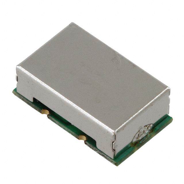
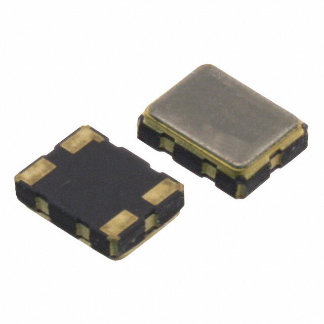
ICGOO在线商城 > 晶体,振荡器,谐振器 > 振荡器 > DOC020F-010.0M
- 型号: DOC020F-010.0M
- 制造商: Connor-Winfield
- 库位|库存: xxxx|xxxx
- 要求:
| 数量阶梯 | 香港交货 | 国内含税 |
| +xxxx | $xxxx | ¥xxxx |
查看当月历史价格
查看今年历史价格
DOC020F-010.0M产品简介:
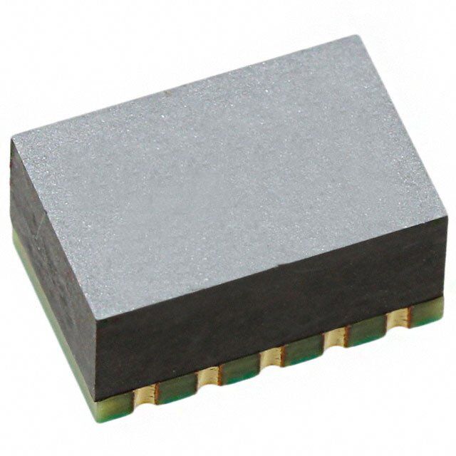
ICGOO电子元器件商城为您提供DOC020F-010.0M由Connor-Winfield设计生产,在icgoo商城现货销售,并且可以通过原厂、代理商等渠道进行代购。 DOC020F-010.0M价格参考。Connor-WinfieldDOC020F-010.0M封装/规格:振荡器, 振荡器 10MHz LVCMOS OCXO 3.3V 6-SMD,无引线。您可以下载DOC020F-010.0M参考资料、Datasheet数据手册功能说明书,资料中有DOC020F-010.0M 详细功能的应用电路图电压和使用方法及教程。
| 参数 | 数值 |
| 产品目录 | 晶体和振荡器 |
| 描述 | OSC OCXO 10.000MHZ LVCMOS SMD |
| 产品分类 | |
| 品牌 | Connor-Winfield |
| 数据手册 | |
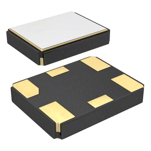
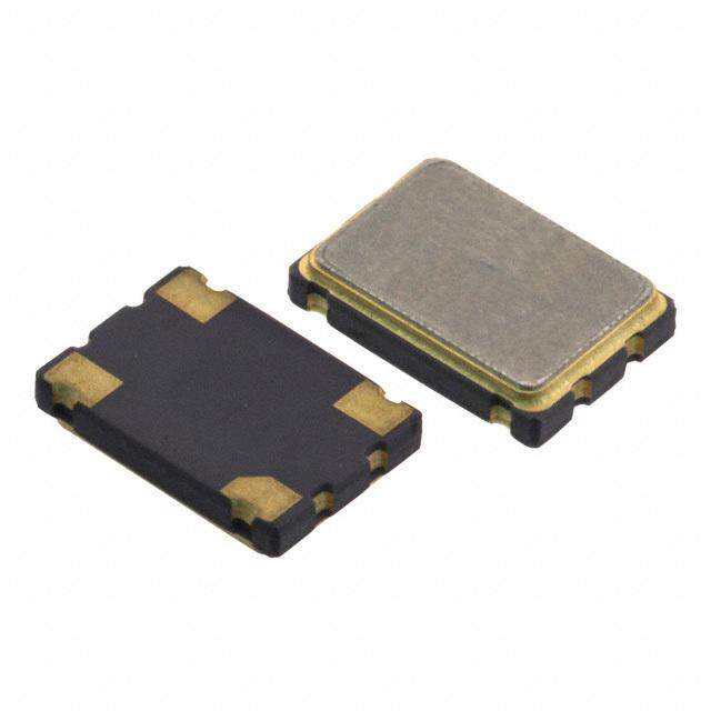
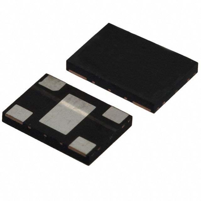
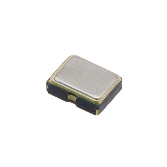
| 产品图片 |
|
| 产品型号 | DOC020F-010.0M |
| PCN设计/规格 | |
| rohs | 无铅 / 符合限制有害物质指令(RoHS)规范要求 |
| 产品系列 | DOC |
| 其它名称 | CW722-2 |
| 功能 | - |
| 包装 | 带卷 (TR) |
| 大小/尺寸 | 0.556" 长 x 0.358" 宽(14.10mm x 9.10mm) |
| 安装类型 | 表面贴装 |
| 封装/外壳 | 6-SMD,无引线(DFN,LCC) |
| 工作温度 | 0°C ~ 70°C |
| 标准包装 | 50 |
| 电压-电源 | 3.3V |
| 电流-电源(最大值) | - |
| 电流-电源(禁用)(最大值) | - |
| 等级 | - |
| 类型 | OCXO |
| 输出 | LVCMOS |
| 频率 | 10MHz |
| 频率稳定度 | ±20ppb |
| 高度 | 0.312" (7.92mm) |




- 商务部:美国ITC正式对集成电路等产品启动337调查
- 曝三星4nm工艺存在良率问题 高通将骁龙8 Gen1或转产台积电
- 太阳诱电将投资9.5亿元在常州建新厂生产MLCC 预计2023年完工
- 英特尔发布欧洲新工厂建设计划 深化IDM 2.0 战略
- 台积电先进制程称霸业界 有大客户加持明年业绩稳了
- 达到5530亿美元!SIA预计今年全球半导体销售额将创下新高
- 英特尔拟将自动驾驶子公司Mobileye上市 估值或超500亿美元
- 三星加码芯片和SET,合并消费电子和移动部门,撤换高东真等 CEO
- 三星电子宣布重大人事变动 还合并消费电子和移动部门
- 海关总署:前11个月进口集成电路产品价值2.52万亿元 增长14.8%
PDF Datasheet 数据手册内容提取
Available at Digi-Key** Surface Mount www.digikey.com Oven Stabilized Oscillator DOC Series OCXO / VCOCXO Description: Features: Connor-Winfield’s high stability DOC series are 2111 Comprehensive Drive • OCXO - Fixed Frequency exceptionally precise frequency 2111 Comprehensive Drive Aurora, Illinois 60505 VCOCXO - Voltage Controlled Option PhoneA: 6u3ro0r-a8,5 I1ll-i4n7o2is2 60505 sint acnedllaurladrs ,b eaxscee sllteantito fnosr ,u tsees t D10O21C800.500FMHz • 3.3 Vdc Operation Fax: 6P3h0o-n8e5:1 6-5300-48051-4722 equipment, Synchronous • SMT Package Fax: 630-851-5040 Ethernet and VSAT applications. • Frequency Stabilities Available: www.conwin.com These true surface mount ±20ppb, ±50ppb, ±100ppb, ±140ppb, ±250ppb www.conwin.com OCXO / VCOCXO oscillators • Temperature Ranges Available: provide frequency stabilities in the range of ±20 0 to 70°C, -20 to 75°, -40 to 85°C or -40 to 70°C ppb to ±250ppb, over the commercial, extended • Low Phase Noise commercial or the industrial temperature range. The DOC series is available with a CMOS • LVCMOS Output output and a Voltage Controlled Option. These • Optional Electronic Frequency Tuning oscillators provide outstanding phase noise • RoHS Compliant / Lead Free characteristics that will meet the most stringent requirements. Suggested Pad Layout Package Outline (90..13m58m) (70.8.300m7m) (10.5.026m0m) 0.085 (90.5.327m5m) 0.085 (2.16mm) (2.16mm) 8Fz 0.060 20H DNC (1.52mm) 05M 0.275 10 (6.99mm) 4 3 C0 0.100 (104..515m5m) DO10. 1 ((220..55.1440mm0mm)) (60.6.206m0m)0.040 5 VTioepw2 0.040 (1.02mm) 6 1 Keep (1.02mm) Out 0.025 DNC DNC=DoNotConnect Area (0.64mm) Top Side Bottom View View View DimensionalTolerance:+/-0.005(0.127mm) Attention: System Designers please review Application Note AN2093: System Design Information and Printed Circuit Board Layout Guidelines for OCXO Oscillators. @ www.conwin.com/support.html Pad Connections 1: N/C or Voltage Control (Vc) 2: Do Not Connect* 3 Ground: 4: Output 5: Do Not Connect* 6: Supply Voltage (Vcc) *DO NOT connect "DNC" pads to ground or supply rails. Ordering Information DOC 05 0 F -010.0M ** Not all Oscillator Frequency Output Type Stability Temperature Voltage Control Frequency options Range Option available at LVCM3.O3 SV dOcutput 0025 == ±±2500 ppppbb 0 = 0 to 70°C F = OCXO FrFeoqrumeantcy *Amount of Digi-Key Surface Mount 10 = ±100 ppb 1 = -20 to 75°C (Fixed Freq.) -xxx.xM Min.* numbers after the Bulletin Cx207 OCXO 1245 == ±±124500 ppppbb 23 == --4400 ttoo 8750°°CC (VVol t=ag Ve CCOonCtrXolOled ) -xxx.xxxxxxM Max* de cMim =a lM pHozint. Page 1 of 4 Example Part Numbers: Revision 22 Date 08 March 2019 DOC05D0OF-C001202.0VM-0 2=0 .90xM1 4=m 9mx 1p4amckmag pea, c±k5a0g ep,p ±b2, 00 ptop b7,0 -°4C0, 3to.3 8 V5d°Cc,, C3.M3 OVdSc O, CutMpuOtS, O OCuXtpOu,t O, VuCtpOuCt FXrOe,q 2u0e.n0c My 1H0z.0 MHz
2111 Comprehensive Drive Aurora, Illinois 60505 Phone: 630-851-4722 Fax: 630-851-5040 www.conwin.com Absolute Maximum Ratings Parameter Minimum Nominal Maximum Units Notes Storage Temperature -55 - 125 °C Supply Voltage - 3.3 Vdc (Vcc) -0.5 - 4.5 Vdc Control Voltage (Vc) -0.5 - Vcc+0.5 Vdc Operating Specifications Parameter Minimum Nominal Maximum Units Notes Center Frequency: (Fo) 10, 12.8, 19.44, 20, 25, 38.88, 40, 49.152, 50 or 80 MHz Frequency Stability vs. Change in Temperature: (See Ordering Information) Stability Code 02 -20 - 20 ppb 1 Stability Code 05 -50 - 50 ppb 1 Stability Code 10 -100 - 100 ppb 1 Stability Code 14 -140 - 140 ppb 1 Stability Code 25 -250 - 250 ppb 1 Operating Temperature Range: (See Ordering Information) Temperature Code 0 0 - 70 °C Temperature Code 1 -20 - 75 °C Temperature Code 2 -40 - 85 °C Temperature Code 3 -40 - 70 °C Frequency Calibration: -1.0 - 1.0 ppm 2 Frequency Stability vs Load -20 - 20 ppb ±5% Frequency Stability vs Voltage -20 - 20 ppb ±5% Aging: Daily: -10 - 10 ppb/day 3 Aging: First Year: -300 - 300 ppb 3 Total Frequency Tolerance (20 Years) -4.60 - 4.60 ppm 4 Supply Voltage: (Vcc) 3.13 3.30 3.47 Vdc 5 Power Consumption: Vcc = Nominal Voltage Commercial Temperature Range, 0 to 70 °C Turn On - - 2.5 W Steady State @ 25°C - - 1.1 W Industrial Temperature Range, -40 to 85 °C Turn On - - 3.0 W Steady State @ 25°C - - 1.3 W Phase Jitter: (BW: 12 KHz to 5MHz @ Fo=49.152MHz) - 0.3 0.35 ps RMS Short Term Stability - - 1.0E-9/s Start-Up Time: - - 10 ms Warm Up Time (Within Specification @ 25°C) - - 60 s Warm Up Time (Within Specification @ -40°C) - - 90 s CMOS Output Characteristics Parameter Minimum Nominal Maximum Units Notes Load - 15 - pF 6 Output Voltage: Output Voltage: High (Voh) 2.7 - - V Low (Vol) - - 0.3 V Output Current: High (Ioh) - - -4 mA Low (Iol) 4 - - mA Duty Cycle at 50% of Vcc 45 50 55 % Rise / Fall Time: 10% to 90% - - 6.5 ns Input Characteristics - Voltage Controlled Option Parameter Minimum Nominal Maximum Units Notes Control Voltage Range: 0.30 1.65 3.00 V 7 Frequency Pullability: ±10.0 - - ppm 8 Input Impedance 100K - - Ohms Linearity ±5 - - % Bulletin Cx207 Attention: System Designers please review Application Note AN2093: Page 2 of 4 System Design Information and Printed Circuit Board Layout Guidelines for OCXO Oscillators. @ Revision 22 www.conwin.com/support.html Date 08 March 2019 Specifications subject to change without notification. See Connor-Winfield's website for latest revision. © Copyright 2019 The Connor-Winfield Corporation Not intended for life support applications.
2111 Comprehensive Drive Aurora, Illinois 60505 Phone: 630-851-4722 Fax: 630-851-5040 www.conwin.com Phase Noise Characteristics Typical Phase Noise for DOC050F - 010.0M Parameter Minimum Nominal Maximum Units Notes @ 1 Hz offset - -67 - dBC/Hz @ 10 Hz offset - -100 - dBC/Hz @ 100 Hz offset - -130 - dBC/Hz @ 1 KHz offset - -148 - dBC/Hz @ 10 KHz offset - -154 - dBC/Hz @ 100 KHz offset - -155 - dBC/Hz Package Characteristics DOC Package Package consisting of a FR-4 substrate and Ryton-R-4 cover. Water Resistant package, non-hermetic seal. (Engineering Properties of Ryton R-4 Application Note AN2100) Environmental Characteristics Shock 500 G’s 1ms, Halfsine, 3 shocks per direction, per MIL-STD 202G, Method 213B Test Condition D. Sinusoidal Vibration 0.06” D.A. or 10G’s Peak, 10 to 500 Hz, per MIL-STD-202G, Method 204D, Test Condition A. Random Vibration 5.35 G’s rms. 20 to 2000 Hz per MIL-STD-202G, Method 214,Test Condition 1A, 15 minutes each axis. Moisture 10 cycles, 95% RH, Per MIL-STD-202G, Method 112. Marking Permanency Per MIL-STD-202G, Method 215J. Solder Process Recommendations: RoHS compliant, lead free. See solder profile on page 4. In-line reflow: Refer to recommended reflow pre-heat and reflow temperatures on page 4. Package material consist of Ryton R-4 high temperature cover with FR4 substrate. Component solder is Pb free high temperature eutectic alloy with a melting point of 221°C.| In-line oven profile: We recommend using KIC profiler or similar device placing one of the thermocouples on the device to insure that the internal package temperature does not exceed 221°C. Removal of device: If for any reason the device needs to be removed from the board, use a temperature controlled repair station with profile monitoring capabilities. Following a monitored profile will insure the device is properly pre-heated prior to relow. Refer to IPC 610E for inspection guidelines. Recommended Cleaning Process: (If required) Device is non-hermetic, water resistance with four weep holes, one in each corner to allow moisture to be removed during the drying cycle. We recommend in-line warm water wash with air knife and drying capabilities. If cleaner does not have drying capability, then use hot air circulated oven. Boards should be placed in the oven vertically for good water runoff Device must be dried properly prior to use! Note: If saponifier is used make sure the device is rinsed properly to insure all residues are removed. PH of saponifier should not exceed 10. Drying Temperature: Between 85 to 100°C. Drying Time: Time will vary depending on the board size. Caution: Do not submerge the device! Notes: 1. Frequency stability vs. change in temperature. [±(Fmax - Fmin)/(2*Fo)]. 2. Initial calibration @ 25°C. For OCXO with EFT, the control voltage must be fixed. 3. After 30 days of operation 4. Inclusive of calibration @ 25°C, frequency vs. change in temperature, change in supply voltage (±5%), load change (±5%), shock and vibration and 20 years aging 5. Minimum "Power On Time" after rail rises from 0 to within +/-5% of Vcc = 1 second. Vcc ramp rate must be <0.3 volts per millisecond. 6. Attention: To achieve optimal frequency stability, and in some cases to meet the specification stated on this data sheet, it is required that the circuit connected to this OCXO output must have the equivalent input capacitance that is specified by the nominal load capacitance. Deviations from the nominal load capacitance will have a graduated effect on the stability of approximately 20 ppb per pF load difference. 7. Positive slope. (Frequency increases as Vc voltage increases. To ensure proper operation of VCOCXO's, the control voltage input must be biased the nominal control voltage. Failure to bias the Vc input will cause an unstable output condition. 8. Referenced to Fo. Bulletin Cx207 Attention: System Designers please review Application Note AN2093: Page 3 of 4 System Design Information and Printed Circuit Board Layout Guidelines for OCXO Oscillators. @ Revision 22 www.conwin.com/support.html Date 08 March 2019 Specifications subject to change without notification. See Connor-Winfield's website for latest revision. © Copyright 2019 The Connor-Winfield Corporation Not intended for life support applications.
2111 Comprehensive Drive Aurora, Illinois 60505 Phone: 630-851-4722 Fax: 630-851-5040 www.conwin.com CMOS Output Waveform CMOS Test Circuit DNC Output 10uF to 0.01uF 100uF 2 15pF Pad1 DNC OCXO=N/C VCOCXO=Vc DNC=DoNotConnect DONOTconnect"DNC"pads 1V/Div togroundorsupplyrails. Phase Noise Plot RoHS Solder Profile TypicalphasenoiseplotforDOC050F-010.0M Temperature 260°C 260°C 220°C 180°C 150°C 120°C 0 10s Upto120s 60to90s Typical Typical MeetsIPC/JEDECJ-STD-020C Tape and Reel Information Bulletin Cx207 Attention: System Designers please review Application Note AN2093: Page 4 of 4 System Design Information and Printed Circuit Board Layout Guidelines for OCXO Oscillators. @ Revision 22 www.conwin.com/support.html Date 08 March 2019 Specifications subject to change without notification. See Connor-Winfield's website for latest revision. © Copyright 2019 The Connor-Winfield Corporation Not intended for life support applications.
 Datasheet下载


