ICGOO在线商城 > 分立半导体产品 > 晶体管 - FET,MOSFET - 单 > DMS3014SFG-7

 Datasheet下载
- 型号: DMS3014SFG-7
- 制造商: Diodes Inc.
- 库位|库存: xxxx|xxxx
- 要求:
| 数量阶梯 | 香港交货 | 国内含税 |
| +xxxx | $xxxx | ¥xxxx |
查看当月历史价格
查看今年历史价格
DMS3014SFG-7产品简介:
ICGOO电子元器件商城为您提供DMS3014SFG-7由Diodes Inc.设计生产,在icgoo商城现货销售,并且可以通过原厂、代理商等渠道进行代购。 DMS3014SFG-7价格参考。Diodes Inc.DMS3014SFG-7封装/规格:晶体管 - FET,MOSFET - 单, 表面贴装 N 沟道 30V 9.5A(Ta) 1W(Ta) PowerDI3333-8。您可以下载DMS3014SFG-7参考资料、Datasheet数据手册功能说明书,资料中有DMS3014SFG-7 详细功能的应用电路图电压和使用方法及教程。
| 参数 | 数值 |
| 产品目录 | |
| 描述 | MOSFET N-CH 30V 9.5A POWERDI |
| 产品分类 | FET - 单 |
| FET功能 | 逻辑电平门 |
| FET类型 | MOSFET N 通道,金属氧化物 |
| 品牌 | Diodes Incorporated |
| 数据手册 | |
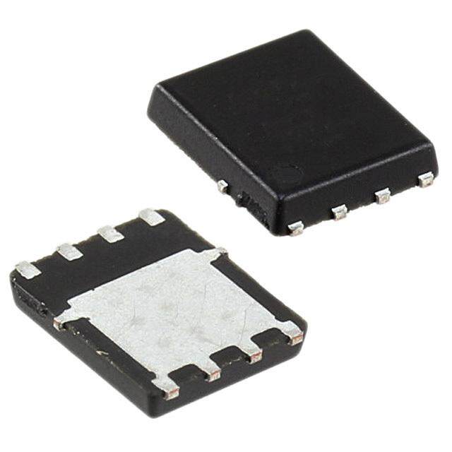
| 产品图片 |
|
| 产品型号 | DMS3014SFG-7 |
| rohs | 无铅 / 符合限制有害物质指令(RoHS)规范要求 |
| RoHS指令信息 | http://diodes.com/download/4349 |
| 产品系列 | - |
| 不同Id时的Vgs(th)(最大值) | 2.2V @ 250µA |
| 不同Vds时的输入电容(Ciss) | 4310pF @ 15V |
| 不同Vgs时的栅极电荷(Qg) | 45.7nC @ 10V |
| 不同 Id、Vgs时的 RdsOn(最大值) | 13 毫欧 @ 10.4A,10V |
| 供应商器件封装 | PowerDI3333-8 |
| 其它名称 | DMS3014SFG-7DICT |
| 功率-最大值 | 1W |
| 包装 | 剪切带 (CT) |
| 安装类型 | 表面贴装 |
| 封装/外壳 | 8-PowerWDFN |
| 标准包装 | 1 |
| 漏源极电压(Vdss) | 30V |
| 电流-连续漏极(Id)(25°C时) | 9.5A (Ta) |


.jpg)


PDF Datasheet 数据手册内容提取
DMS3014SFG 30V N-CHANNEL ENHANCEMENT MODE MOSFET POWERDI® Product Summary Features and Benefits N O V(BR)DSS RDS(ON) max ID max • iDnItOegFrEaTte uat ilMizOesS aF EuTn iqauned paa Stecnhtoetdtk py rionc ae sssin tgol em doineo tloit hdieclaivlley r: I TA = 25°C • Low R – minimize conduction losses T DS(ON) A 13mΩ @ VGS = 10V 9.5A • Low VSD – reducing the losses due to body diode conduction M 30V • Low Qrr – lower Qrr of the integrated Schottky reduces body R 14mΩ @ VGS = 4.5V 9.0A diode switching losses • Low gate capacitance (Q/Q ) ratio – reduces risk of shoot- O g gs through or cross conduction currents at high frequencies F • Small form factor thermally efficient package enables higher N density end products I E • Occupies just 33% of the board area occupied by SO-8 enabling smaller end product C N • 100% UIS (Avalanche) rated A • 100% Rg tested V • Totally Lead-Free & Fully RoHS Compliant (Notes 1 & 2) D • Halogen and Antimony Free. “Green” Device (Note 3) A • Qualified to AEC-Q101 Standards for High Reliability Description and Applications Mechanical Data This MOSFET has been designed to minimize the on-state resistance • Case: POWERDI3333-8 (RDS(on)) and yet maintain superior switching performance, making it • Case Material: Molded Plastic, "Green" Molding Compound. ideal for high efficiency power management applications. UL Flammability Classification Rating 94V-0 • Moisture Sensitivity: Level 1 per J-STD-020 • Backlighting • Terminal Connections Indicator: See diagram • Power Management Functions • Terminals: Finish ⎯ Matte Tin annealed over Copper leadframe. • DC-DC Converters Solderable per MIL-STD-202, Method 208 • Weight: 0.072 grams (approximate) Drain S Pin 1 8 7 6 5 S S G Gate D D D D 1 2 3 4 Source Top View Bottom View Top View Pin Configuration Internal Schematic Ordering Information (Note 4) Part Number Case Packaging DMS3014SFG-7 POWERDI3333-8 2000/Tape & Reel DMS3014SFG-13 POWERDI3333-8 3000/Tape & Reel Notes: 1. No purposely added lead. Fully EU Directive 2002/95/EC (RoHS) & 2011/65/EU (RoHS 2) compliant. 2. See http://www.diodes.com for more information about Diodes Incorporated’s definitions of Halogen- and Antimony-free, "Green" and Lead-free. 3. Halogen- and Antimony-free "Green” products are defined as those which contain <900ppm bromine, <900ppm chlorine (<1500ppm total Br + Cl) and <1000ppm antimony compounds. 4. For packaging details, go to our website at http://www.diodes.com. POWERDI is a registered trademark of Diodes Incorporated DMS3014SFG 1 of 8 May 2012 Document number: DS35594 Rev. 6 - 2 www.diodes.com © Diodes Incorporated
DMS3014SFG Marking Information N O TI WW S29 = Product Type Marking Code Y YYWW = Date Code Marking A Y YY = Last digit of year (ex: 11 = 2011) M S29 WW = Week code (01 ~ 53) R O F N I E Maximum Ratings @TA = 25°C unless otherwise specified C Characteristic Symbol Value Units N A Drain-Source Voltage VDSS 30 V V Gate-Source Voltage VGSS ±12 V AD Continuous Drain Current (Note 6) VGS = 10V StS<tet1aa0tdesy TTTTAAAA ==== 27275050°°°°CCCC IIDD 19793....5670 AA Continuous Drain Current (Note 6) VGS = 4.5V StS<tet1aa0tdesy TTTTAAAA ==== 27275050°°°°CCCC IIDD 19792....0432 AA Pulsed Drain Current (10μs pulse, duty cycle = 1%) IDM 80 A Maximum Continuous Body Diode Forward Current (Note 6) IS 3.0 A Avalanche Current (Note 7) L = 0.1mH IAR 30 A Repetitive Avalanche Energy (Note 7) L = 0.1mH EAR 45 mJ Thermal Characteristics @TA = 25°C unless otherwise specified Characteristic Symbol Value Units Total Power Dissipation (Note 5) PD 1 W Steady state 131 °C/W Thermal Resistance, Junction to Ambient (Note 5) t<10s RθJA 72 °C/W Total Power Dissipation (Note 6) PD 2.1 W Steady state 63 °C/W Thermal Resistance, Junction to Ambient (Note 6) t<10s RθJA 35 °C/W Thermal Resistance, Junction to Case (Note 6) RθJC 7.1 °C/W Operating and Storage Temperature Range TJ, TSTG -55 to +150 °C Notes: 5. Device mounted on FR-4 substrate PC board, 2oz copper, with minimum recommended pad layout. 6. Device mounted on FR-4 substrate PC board, 2oz copper, with 1inch square copper plate. 7. I and E rating are based on low frequency and duty cycles to keep T = 25°C AR AR J POWERDI is a registered trademark of Diodes Incorporated DMS3014SFG 2 of 8 May 2012 Document number: DS35594 Rev. 6 - 2 www.diodes.com © Diodes Incorporated
DMS3014SFG 100 100 RDS(on) PW = 10µs 90 N Limited W) Single Pulse O R ( 80 RθJA = 61°C/W ATI NT (A) 10 POIWE 70 RTJθ J-A T(tA) == rP(t )* * R RθθJJAA(t) M RE DC NT 60 NFOR RAIN CUR 1 PW =P 1WP0 W=s 1=sP 1W0 0=m 1s0ms TRANSIE 4500 E I -I, DD 0.1 PWP W= 1=m 1s00µs PEAK 30 C TJ(max) = 150°C , K) 20 N TSAin =gl e2 5P°uClse P(P 10 A V 0.01 0 0.1 1 10 100 0.0001 0.001 0.01 0.1 1 10 100 1,000 D -VDS, DRAIN-SOURCE VOLTAGE (V) t1, PULSE DURATION TIME (sec) A Fig. 1 SOA, Safe Operation Area Fig. 2 Single Pulse Maximum Power Dissipation 1 D = 0.9 E D = 0.7 C D = 0.5 N A T D = 0.3 S SI RE 0.1 L D = 0.1 A M R D = 0.05 E H T T D = 0.02 N E 0.01 SI D = 0.01 N A TR D = 0.005 RθJA(t) = r(t) * RθJA r(t), D = Single Pulse RDθuJtyA C= y6c0le°C, D/W = t1/t2 0.001 0.00001 0.0001 0.001 0.01 0.1 1 10 100 1,000 t1, PULSE DURATION TIME (sec) Fig. 3 Transient Thermal Resistance POWERDI is a registered trademark of Diodes Incorporated DMS3014SFG 3 of 8 May 2012 Document number: DS35594 Rev. 6 - 2 www.diodes.com © Diodes Incorporated
DMS3014SFG Electrical Characteristics TA = 25°C unless otherwise specified N Characteristic Symbol Min Typ Max Unit Test Condition O OFF CHARACTERISTICS (Note 8) TI Drain-Source Breakdown Voltage BVDSS 30 - - V VGS = 0V, ID = 250μA A Zero Gate Voltage Drain Current IDSS - - 100 μA VDS = 30V, VGS = 0V M Gate-Source Leakage IGSS - - ±100 nA VGS = ±12V, VDS = 0V ON CHARACTERISTICS (Note 8) R O Gate Threshold Voltage VGS(th) 1.0 - 2.2 V VDS = VGS, ID = 250μA NF Static Drain-Source On-Resistance RDS (ON) -- 190 1143 mΩ VVGGSS == 14.05VV,, I DID == 1100..44AA I Forward Transfer Admittance |Yfs| - 23 - S VDS = 5V, ID = 10.4A E Diode Forward Voltage VSD - 0.4 0.55 V VGS = 0V, IS = 1A C DYNAMIC CHARACTERISTICS (Note 9) N Input Capacitance Ciss - 2296 4310 pF A Output Capacitance Coss - 164 - pF fV =D S1 .=0 M15HVz, VGS = 0V, V Reverse Transfer Capacitance Crss - 120 - pF D Gate Resistance Rg 0.26 1.3 2.34 Ω VDS = 0V, VGS = 0V, f = 1MHz A Total Gate Charge VGS = 4.5V Qg - 19.3 - nC TGoattael- SGoauterc Ce hCahrgaerg VeG S = 10V QQggs -- 455.0.7 -- nnCC VDS = 15V, VGS = 10V, ID = 10.4A Gate-Drain Charge Qgd - 2.9 - nC Turn-On Delay Time tD(on) - 5.5 - ns Turn-On Rise Time tr - 24.4 - ns VGS = 10V, VDS = 15V, Turn-Off Delay Time tD(off) - 33.1 - ns RG = 3Ω, RL = 1.2Ω Turn-Off Fall Time tf - 6.6 - ns Reverse Recovery Time trr - 12.9 - ns IF = 13A, di/dt = 500A/μs Reverse Recovery Charge Qrr - 8.0 - nC IF = 13A, di/dt = 500A/μs Notes: 8. Short duration pulse test used to minimize self-heating effect. 9. Guaranteed by design. Not subject to product testing. 30 30 VGS = 4.5V VGS = 4.0V VDS = 5V 25 VGS = 3.5V 25 VGS = 2.5V A) A) T ( 20 T ( 20 N N E E RR VGS = 3.0V RR U 15 U 15 VGS = 150°C C C AIN AIN VGS = 125°C DR 10 DR 10 VGS = 85°C , D , D I I 5 VGS = 2.2V 5 VGS = 25°C VGS = 2.0V VGS = -55°C 0 0 0 0.5 1 1.5 2 0 0.5 1 1.5 2 2.5 3 V , DRAIN-SOURCE VOLTAGE (V) V , GATE-SOURCE VOLTAGE (V) DS GS Fig. 4 Typical Output Characteristic Fig. 5 Typical Transfer Characteristic POWERDI is a registered trademark of Diodes Incorporated DMS3014SFG 4 of 8 May 2012 Document number: DS35594 Rev. 6 - 2 www.diodes.com © Diodes Incorporated
DMS3014SFG )Ω 0.05 )Ω 0.04 E ( E ( VGS = 4.5V C C N N N STA 0.04 STA 0.03 O ESI ESI TI N-R 0.03 N-R MA RCE O VGS = 2.5V RCE O 0.02 TTAA == 115205°°CC OR SOU 0.02 SOU TA = 85°C NF RAIN- VGS = 4.5V RAIN- 0.01 TA = 25°C E I , DON)0.01 VGS = 10V , DN) TA = -55°C C DS( S(O N R 0 RD 0 0 5 10 15 20 25 30 0 5 10 15 20 25 30 A I , DRAIN-SOURCE CURRENT (A) I , DRAIN CURRENT (A) V D D Fig. 6 Typical On-Resistance Fig. 7 Typical On-Resistance D vs. Drain Current and Gate Voltage vs. Drain Current and Temperature A 1.6 0.03 ))ΩΩ V = 4.5V E (E ( D) IGS = 10A NCNC E 1.4 D AA RCE MALIZ VGS = 10V ESISTESIST 0.02 UR I = 20A RR R, DRAIN-SODSONRESISTANCE (NO 11..02 D AIN-SOURCE ON-AIN-SOURCE ON- 0.01 VIGDS = = 1 40.A5VVIGDS = = 2 100AV N- 0.8 DRDR O , , NN OO SS DD RR 0.6 0 -50 -25 0 25 50 75 100 125 150 -50 -25 0 25 50 75 100 125 150 TA, AMBIENT TEMPERATURE (°C) TA, AMBIENT TEMPERATURE (°C) Fig. 8 On-Resistance Variation with Temperature Fig. 9 On-Resistance Variation with Temperature 3.0 20 V) 18 E ( 2.5 G 16 A LT A) VO 2.0 NT ( 14 LD RE 12 TA = 25°C O R H U S 1.5 C 10 RE ID = 10mA E TH RC 8 ATE 1.0 SOU 6 , GH) I, S 4 T 0.5 S( G 2 V 0 0 -50 -25 0 25 50 75 100 125 150 0 0.2 0.4 0.6 0.8 1.0 1.2 T , AMBIENT TEMPERATURE (°C) V , SOURCE-DRAIN VOLTAGE (V) A SD Fig. 10 Gate Threshold Variation vs. Ambient Temperature Fig. 11 Diode Forward Voltage vs. Current POWERDI is a registered trademark of Diodes Incorporated DMS3014SFG 5 of 8 May 2012 Document number: DS35594 Rev. 6 - 2 www.diodes.com © Diodes Incorporated
DMS3014SFG 10,000 10,000 f = 1MHz N A) TA = 125°C µ TIO E (pF) 1,000 Ciss RENT (1,000 A NC UR TA = 85°C M A C OR PACIT Coss KAGE 100 INF C, CA 100 Crss , LEASS 10 E ID TA = 25°C C N A 10 1 0 5 10 15 20 25 30 0 10 20 30 V D VDS, DRAIN-SOURCE VOLTAGE (V) VDS, DRAIN-SOURCE VOLTAGE (V) Fig. 12 Typical Total Capacitance Fig. 13 Typical Leakage Current A vs. Drain-Source Voltage 10 9 V) E( 8 G A 7 T L E VO 6 VIDD S= 1=1 1.25AV C R 5 U O S 4 E- AT 3 G , S 2 G V 1 0 0 5 10 15 20 25 30 35 40 45 Q , TOTAL GATE CHARGE (nC) g Fig. 14 Gate-Source Voltage vs. Total Gate Charge POWERDI is a registered trademark of Diodes Incorporated DMS3014SFG 6 of 8 May 2012 Document number: DS35594 Rev. 6 - 2 www.diodes.com © Diodes Incorporated
DMS3014SFG Package Outline Dimensions N O I T POWERDI3333-8 MA A A3 Dim Min Max Typ A1 D 3.25 3.35 3.30 R D E 3.25 3.35 3.30 O D2 2.22 2.32 2.27 D2 F E2 1.56 1.66 1.61 N L A 0.75 0.85 0.80 (4x) E I Pin 1 ID 1 4 AA13 0− 0.−0 5 00.2.0023 NC E (b42x) bb2 0.−2 7 0.−3 7 00..3220 A E2 L 0.35 0.45 0.40 V 8 5 L1 − − 0.39 D (L31x) e − − 0.65 A Z − − 0.515 All Dimensions in mm Z (4x) e b (8x) Suggested Pad Layout X G Dimensions Value (in mm) C 0.650 G 0.230 8 5 G1 0.420 Y2 G1 Y1 Y 3.700 Y Y1 2.250 Y2 1.850 Y3 0.700 1 4 X 2.370 Y3 X2 0.420 X2 C POWERDI is a registered trademark of Diodes Incorporated D MS3014SFG 7 of 8 May 2012 D ocument number: DS35594 Rev. 6 - 2 www.diodes.com © Diodes Incorporated
DMS3014SFG IMPORTANT NOTICE N DIODES INCORPORATED MAKES NO WARRANTY OF ANY KIND, EXPRESS OR IMPLIED, WITH REGARDS TO THIS DOCUMENT, O INCLUDING, BUT NOT LIMITED TO, THE IMPLIED WARRANTIES OF MERCHANTABILITY AND FITNESS FOR A PARTICULAR PURPOSE I (AND THEIR EQUIVALENTS UNDER THE LAWS OF ANY JURISDICTION). T A Diodes Incorporated and its subsidiaries reserve the right to make modifications, enhancements, improvements, corrections or other changes M without further notice to this document and any product described herein. Diodes Incorporated does not assume any liability arising out of the R application or use of this document or any product described herein; neither does Diodes Incorporated convey any license under its patent or trademark rights, nor the rights of others. Any Customer or user of this document or products described herein in such applications shall assume O all risks of such use and will agree to hold Diodes Incorporated and all the companies whose products are represented on Diodes Incorporated F website, harmless against all damages. N I Diodes Incorporated does not warrant or accept any liability whatsoever in respect of any products purchased through unauthorized sales channel. E Should Customers purchase or use Diodes Incorporated products for any unintended or unauthorized application, Customers shall indemnify and C hold Diodes Incorporated and its representatives harmless against all claims, damages, expenses, and attorney fees arising out of, directly or N indirectly, any claim of personal injury or death associated with such unintended or unauthorized application. A Products described herein may be covered by one or more United States, international or foreign patents pending. Product names and markings V noted herein may also be covered by one or more United States, international or foreign trademarks. D A LIFE SUPPORT Diodes Incorporated products are specifically not authorized for use as critical components in life support devices or systems without the express written approval of the Chief Executive Officer of Diodes Incorporated. As used herein: A. Life support devices or systems are devices or systems which: 1. are intended to implant into the body, or 2. support or sustain life and whose failure to perform when properly used in accordance with instructions for use provided in the labeling can be reasonably expected to result in significant injury to the user. B. A critical component is any component in a life support device or system whose failure to perform can be reasonably expected to cause the failure of the life support device or to affect its safety or effectiveness. Customers represent that they have all necessary expertise in the safety and regulatory ramifications of their life support devices or systems, and acknowledge and agree that they are solely responsible for all legal, regulatory and safety-related requirements concerning their products and any use of Diodes Incorporated products in such safety-critical, life support devices or systems, notwithstanding any devices- or systems-related information or support that may be provided by Diodes Incorporated. Further, Customers must fully indemnify Diodes Incorporated and its representatives against any damages arising out of the use of Diodes Incorporated products in such safety-critical, life support devices or systems. Copyright © 2012, Diodes Incorporated www.diodes.com POWERDI is a registered trademark of Diodes Incorporated DMS3014SFG 8 of 8 May 2012 Document number: DS35594 Rev. 6 - 2 www.diodes.com © Diodes Incorporated
Mouser Electronics Authorized Distributor Click to View Pricing, Inventory, Delivery & Lifecycle Information: D iodes Incorporated: DMS3014SFG-7